Note: Descriptions are shown in the official language in which they were submitted.
CA 02744966 2011-05-27
WO 2010/064108 PCT/IB2009/007593
-1-
SWITCHING APPARATUS COMPRISING A PLURALITY OF
SWITCHING ASSEMBLIES, AND ASSOCIATED METHOD
BACKGROUND OF THE INVENTION
Field of the Invention
This invention relates to electrical switching apparatus and, more
particularly, to circuit interrupters, such as, for example, aircraft or
aerospace circuit
breakers providing arc fault protection. The invention also relates to an
electrical
switching. apparatus that comprises a plurality of circuit interrupters that
are
configured for simultaneous operation.
Background Information
Circuit breakers are used to protect electrical circuitry from damage
due to an'overcurrent condition, such as an overload condition or a relatively
high
level short circuit or fault condition. In small circuit breakers, commonly
referred to
as miniature circuit breakers,-used for residential and light commercial
applications,
such protection is typically provided by a thermal-magnetic trip device. This
trip
device includes a bimetal, which heats and bends in response to a persistent
overcurrent condition. The bimetal, in turn, unlatches a spring powered
operating
mechanism, which opens the separable contacts of the circuit breaker to
interrupt
current flow in the protected power system.
Subminiature circuit breakers are used, for example, in aircraft or
aerospace electrical systems where they not only provide overcurrent
protection but
also serve as switches for turning equipment on and off. Such circuit breakers
must
be small to accommodate the high-density layout of circuit breaker panels,
which
make circuit breakers for numerous circuits accessible to a user. Aircraft
electrical
systems, for example, usually consist of hundreds of circuit breakers, each of
which is
used for a circuit protection function as well as a circuit disconnection
function
through a push-pull handle. Difficulty exists in developing and employing the
wide
variety of circuit breaker solutions that may be required for any given
aircraft.
Typically, subminiature circuit breakers have provided protection
against persistent overcurrents implemented by a latch triggered by a bimetal
responsive to 12 R heating resulting from the overcurrent. There is a growing
interest
in providing additional protection, and most importantly arc fault protection.
CA 02744966 2011-05-27
WO 2010/064108 PCT/IB2009/007593
-2-
During sporadic arc fault conditions, the overload capability of the
circuit breaker will not function since the root-mean-squared (RMS) value of
the fault
current is too small to actuate the automatic trip circuit. The addition of
electronic arc
fault sensing to a circuit breaker can add one of the elements required for
sputtering
arc fault protection - ideally, the output of an electronic arc fault sensing
circuit
directly trips and, thus, opens the circuit breaker. See, for example, U.S.
Patent Nos.
6,710,688; 6,542,056; 6,522,509; 6,522,228; 5,691,869; and 5,224,006.
Common methods of actuating a test function on, for example, a circuit
breaker, include employing a mechanical pushbutton switch. See, for example,
U.S.
Patent Nos. 5,982,593;.5,459,630; 5,293,522; 5,260,676; and 4,081,852.
However,
such mechanical mechanisms often fail due to mechanical stress and may be
actuated
by mistake. Furthermore, such mechanical mechanisms, when employed on a
relatively small circuit breaker, such as, for example, a sub-miniature
circuit breaker,
are of relatively large size.
Proximity sensors include, for example, Hall effect sensors. These
sensors, used in automatic metal detectors, change their electrical
characteristics when
exposed to a magnet. Usually, such sensors have three wires for supply
voltage,
signal and ground.
There is room for improvement in electrical switching apparatus
employed in certain applications.
SUMMARY OF THE INVENTION
These needs and others are met by the present invention, which
provides an electrical switching apparatus that comprises a plurality of
electrical
switching assemblies in the form of miniature circuit breakers that are in a
ganged-
together configuration. Other needs are met by an improved method of using the
electrical switching apparatus.
An aspect of the invention is to configure an electrical switching
apparatus out of a plurality of electrical switching assemblies, and the
electrical
switching assemblies can have different nominal load capacities.
Another aspect of the invention is to provide an electrical switching
apparatus having a plurality of electrical switching assemblies that are
bridged
together for simultaneous operation.
CA 02744966 2011-05-27
WO 2010/064108 PCT/IB2009/007593
-3-
Another aspect of the invention, therefore, is to provide an electrical
switching apparatus, the general nature of which can be stated as comprising a
plurality of electrical switching assemblies, a connection assembly, and a
bridging
device. The electrical switching assemblies each comprise a housing, separable
contacts, an operating mechanism structured to open and close the separable
contacts,
an elongated actuator device translatable along its direction of elongation
between
OFF and ON positions and cooperating with the operating mechanism to open and
close the separable contact, and a trip assembly cooperating with the
operating
mechanism to trip open the separable contacts. The connection assembly is
structured
to mechanically connect together the electrical switching assemblies. The
bridging
device is structured to mechanically connect together the actuator devices.
An inventive method of interrupting at least a portion of a circuit with
the electrical switching apparatus can be generally stated as comprising
triggering
with the trip assembly of one of the electrical switching assemblies its
operating
mechanism to trip open its separable contacts and to translate its actuator
device
toward its OFF position, and employing the bridging device to move the
actuator
devices of the other electrical switching assemblies toward their OFF
positions and to
open their separable contacts.
BRIEF DESCRIPTION OF THE DRAWINGS
A full understanding of the invention can be gained from the following
description of the preferred embodiments when read in conjunction with the
accompanying drawings in which:
Figure 1 is a block diagram of a circuit breaker in accordance with the
present invention.
Figure 2 is a block diagram in schematic form of a processor, power
supply, active rectifier and gain stage, peak detector and Hall effect sensor
of Figure
1.
Figure 3 is an exploded view of an electrical switching apparatus that
employs the circuit breaker of Figure 1.
Figure 4 is front elevational view of the electrical switching apparatus
of Figure 3 mounted to a panel and in an ON position.
CA 02744966 2011-05-27
WO 2010/064108 PCT/IB2009/007593
-4-
Figure 5 is a view similar to Figure 4, except depicting the electrical
switching apparatus in an OFF or TRIPPED position.
Figure 6 is a view similar to Figure 5, except depicting one of the
circuit breakers displaying an indicator that is indicative of an arc fault
condition.
Figure 7 is an exploded view of a fastener assembly of the electrical
switching apparatus of Figure 3.
DESCRIPTION OF THE PREFERRED EMBODIMENTS
The present invention is described in association with an aircraft or
aerospace arc fault circuit breaker, although the invention is applicable to a
wide
range of electrical switching apparatus, such as, for example, circuit
interrupters
adapted to detect a wide range of faults,=such as, for example, arc faults or
ground
faults in power circuits.
Referring to Figure 1, an electrical switching assembly in the form of
an arc fault circuit breaker 1 is connected in an electric power system 11
which has a
line conductor (L) 13 and a neutral conductor (N) 15. The circuit breaker 1
includes
separable contacts 17 which are electrically connected in the line conductor
13. The
separable contacts 17 are opened and closed by an operating mechanism 19. In
addition to being operated manually by a handle (not shown), the operating
mechanism 19 can also be actuated to open the separable contacts 17 by a trip
assembly 21. This trip assembly 21 includes the conventional bimetal 23 which
is
heated by persistent overcurrents and bends to actuate the operating mechanism
19 to
open the separable contacts 17. An armature 25 in the trip assembly 21 is
attracted by
the large magnetic force generated by very high overcurrents to also actuate
the
operating mechanism 19 and provide an instantaneous trip function.
The circuit breaker 1 is also provided with an arc fault detector (AFD)
27. The AFD 27 senses the current in the electrical system 11 by monitoring
the
voltage across the bimetal 23 through the lead 31 with respect to local ground
reference 47. If the AFD 27 detects an arc fault in the electric power system
11, then
a trip signal 35 is generated which turns on a switch such as the silicon
controlled
rectifier (SCR) 37 to energize a trip solenoid 39. The trip solenoid 39 when
energized
actuates the operating mechanism 19 to open the separable contacts 17. A
resistor 41
in series with the coil of the solenoid 39 limits the coil current and a
capacitor 43
CA 02744966 2011-05-27
WO 2010/064108 PCT/IB2009/007593
-5-
protects the gate of the SCR 37 from voltage spikes and false tripping due to
noise.
Alternatively, the resistor 41 need not be employed.
The AFD 27 cooperates with the operating mechanism 19 to trip open
the separable contacts 17 in response to an arc fault condition. The AFD 27
includes
an active rectifier and gain stage 45, which rectifies and suitably amplifies
the voltage
across the bimetal 23 through the lead 31 and the local ground reference 47.
The
active rectifier and gain stage 45 outputs a rectified signal 49 on output 51
representative of the current in the bimetal 23. The rectified signal 49 is
input by a
peak detector circuit 53 and a microcontroller ( C) 55.
The active rectifier and gain stage 45 and the peak detector circuit. 53
form a first circuit 57 adapted to determine a peak amplitude 59 of a
rectified
alternating current pulse based upon the current flowing in the electric power
system
11. The peak amplitude 59 is stored by the peak detector circuit 53.
The C 55 includes an analog-to-digital converter (ADC) 61, a
microprocessor ( P) 63 and a comparator 65. The P 63 includes one or more arc
fault algorithms 67. The ADC 61 converts the analog peak amplitude 59 of the
rectified alternating current pulse to a corresponding digital value for input
by the P
63. The P 63, arc fault algorithm(s) 67 and ADC 61 form a second circuit 69
adapted to determine whether the peak amplitude of the current pulse is
greater than a
predetermined magnitude. In turn, the algorithm(s) 67 responsively employ the
peak
amplitude to determine whether an arc fault condition exists in the electric
power
system 11.
The P 63 includes an output 71 adapted to reset the peak detector
circuit 59. The second circuit 69 also includes the comparator 65 to determine
a
change of state (or a negative (i.e., negative-going) zero crossing) of the
alternating
current pulse of the current flowing in the electric power system 11 based
upon the
rectified signal 49 transitioning from above or below (or from above to below)
a
suitable reference 73 (e.g., a suitable positive value of slightly greater
than zero).
Responsive to this negative zero crossing, as determined by the comparator 65,
the P
63 causes the ADC 61 to convert the peak amplitude 59 to a corresponding
digital
value.
CA 02744966 2011-05-27
WO 2010/064108 PCT/IB2009/007593
-6-
The example arc fault detection method employed by the AFD 27 is
"event-driven" in that it is inactive (e.g., dormant) until a current pulse
occurs as
detected by the comparator 65. When such a current pulse occurs, the
algorithm(s) 67
record the peak amplitude 59 of the current pulse as determined by the peak
detector
circuit 53 and the ADC 61, along with the time since the last current pulse
occurred as
measured by a timer (not shown) associated with the .tP 63. The arc fault
detection
method then uses the algorithm(s) 67 to process the current amplitude and time
information to determine whether a hazardous arc fault condition exists.
Although an
example AFD method and circuit are shown, the invention is applicable to a
wide
range of AFD methods and circuits. See, for example, U.S. Patent Nos.
6,710,688;
6,542,056; 6,522,509; 6,522,228; 5,691,869; and 5,224,006.
An output 100 of a suitable proximity sensor, such as, for example and
without limitation, a Hall effect sensor 101, is held "high" by a pull-up
resistor 103.
When the Hall effect sensor 101 is actuated, for example, by a suitable
target, such as
for example and without limitation, a magnetic wand 105, the sensor output 100
is
driven low (e.g., by an open drain output). When the P 63 determines that the
input
107 is low, it outputs a suitable pulse train signal 109 on output 111. That
signal 109
is fed back into the input of the active rectifier and gain stage 45. In turn,
the pulse
train signal 109 causes the AFD algorithms 67 to determine that there is an
arc fault
trip condition, albeit a test condition, such that the trip signal 35 is set.
A blocking
diode 113 is employed to prevent any current from flowing into the P output
111.
Figure 2 is a block diagram in schematic form of the C 55, power
supply 77, active rectifier and gain stage 45, peak detector 53 and Hall
effect sensor
101 of Figure 1. The C 55 may be, for example, a suitable processor, such as
model
PIC 16F676 marketed by Microchip Technology Inc. of Chandler, Arizona. A
digital
output 79 includes the trip signal 35. An analog input 81 receives the peak
amplitude
59 for the ADC 61 (Figure 1). Digital input RCO of gC 55 is employed to read
the
output (COUT) of the comparator 65. Another digital input RC2 107 of gC 55 is
employed to read the sensor output 100. Another digital output RC5 111 of C
55
includes the pulse train signal 109 to simulate an arc fault trip condition
responsive to
the sensing the wand 105 with the sensor 101. The C 55, thus, forms an arc
fault trip
CA 02744966 2011-05-27
WO 2010/064108 PCT/IB2009/007593
-7-
mechanism including a test circuit adapted to simulate an arc fault trip
condition to
trip open the separable contacts 17 (Figure 1).
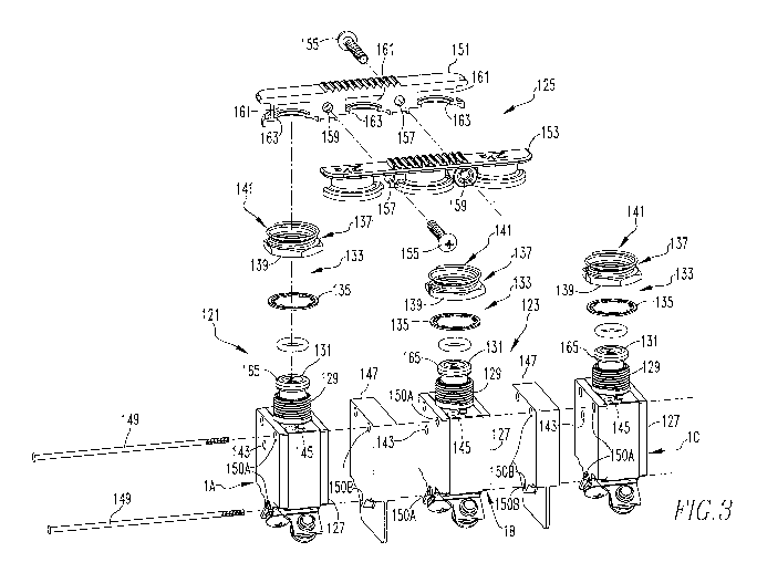
Figure 3 is an exploded view of an improved electrical switching
apparatus in the form of an aircraft or aerospace circuit breaker apparatus
121 that
comprises a plurality of the circuit breakers 1 that are indicated at the
numerals 1 A,
1 B, and 1 C in Figure 3. It is noted that the circuit breakers 1 A, 1 B, and
1 C may be
different than the circuit breaker 1 without departing from the present
concept.
In addition to the circuit breakers 1 A, 1 B, and 1C, the circuit breaker
apparatus 121 comprises a connection assembly 123 and a bridging device 125.
The
connection assembly 123 can be said to mechanically connect together or gang
the.
circuit breakers 1 A, 1 B, and 1 C. The bridging device 125 can be said to
operationally
connect together or gang the circuit breakers 1 A, 1 B, and 1 C, it being
further noted
that the bridging device 125 also mechanically connects together at least a
portion of
each of the circuit breakers 1 A, 1 B, and 1 C.
As is depicted in Figure 3, the circuit breakers 1 A, 113, and 1 C can
each be said to include a housing 127 upon which is disposed a threaded
connector
129, an elongated actuator device 131 that is translatable along its direction
of
elongation between an ON position and an OFF or TRIPPED position, and a
securement assembly 133 that is cooperable with the threaded connector 129 for
mounting the circuit breaker apparatus 121 to a panel 166 (Figures 4-6) or
other
support.
As can be further seen in Figure 3, the securement assembly 133
includes a lock washer 135 and a fastener assembly 137. The fastener assembly
137
comprises a fastener 139 in the exemplary form of a nut and a biasing device
in the
exemplary form of a conical spring 141 coupled together.
The circuit breakers 1 A, 1 B, and 1 C further each include an
illumination element 143 situated on the housing 127 which, when illuminated,
indicates that certain aspects of the circuit breaker 1 A, 1 B, and 1 C are
operational.
The circuit breakers 1 A, 1 B, and 1C further each include a proximity sensor
145
which is structured to sense a magnetic target (not expressly depicted
herein). The
proximity sensor 145 in the exemplary embodiment depicted herein is the Hall
effect
sensor 101 of Figures 1 and 2.
CA 02744966 2011-05-27
WO 2010/064108 PCT/IB2009/007593
-8-
As can further be seen in Figure 3, the connection assembly 123
includes a pair of spacers 147 and a pair of pins 149. The spacers 147 are
formed of a
material that is at least partially translucent and that is structured to
transmit the
visible light generated by the illumination elements 143. The pins 149 are
received
through holes 150A formed in the housings 127 and through holes 150B formed in
the
spacers 147 to connect together the circuit breakers 1 A, 1 B, and 1 C and the
spacers
147 in a ganged configuration. The pins 149 can be secured in the holes 150A
and
150B in any of a variety of fashions, such as by flaring the free end of the
pins 149
opposite the heads thereof, or in other fashions.
The bridging device 125 can be seen in Figure 3 as comprising a first
member 151 and a second member 153 that are connected together with fasteners
155
that are in the exemplary form of a machine screws. In the exemplary
embodiment
depicted herein, each fastener 155 is received through a thru-bore 157 formed
in the
first member 151 or the second members 153 and is threadably received in
threaded
insert 159 that is disposed on the other of the first member 1151 and the
second
member 153.
It can be seen that the bridging device 125 is formed with a number of
receptacles 161 formed in the first and second members 151 and 153 that each
include, in the exemplary embodiment depicted herein, a bracing wall 163. When
assembled, the flared ends 165 of the actuator device 131 are received in the
receptacles 161, with the flared end 165 engaging the bracing wall 163 to
securely
and mechanically connect together the actuator devices 131 with the bridging
device
125.
The circuit breaker apparatus 121 is depicted in Figures 4, 5, and 6 as
being in an assembled condition mounted to a panel 166, such as that of an
aircraft or
other device. The threaded connectors 129 are received through openings 167
formed
in the panel 166. The lock washers 135 and fastener assemblies 137 are
received on
the threaded connectors 129, with the lock washer 135 being interposed between
the
fastener assembly 137 and a face of the panel 166. The bridging device 125 is
then
connected to the actuator devices 131 by receiving the flared ends 165 thereof
in the
receptacles 161 and receiving the fasteners 155 through the thru-bores 157 and
the
threaded inserts 159. Optionally, a resilient member may be further received
in the
CA 02744966 2011-05-27
WO 2010/064108 PCT/IB2009/007593
-9-
receptacles 161 if needed to tightly brace the flared ends 165 against the
bracing walls
163.
As mentioned above, the circuit breaker apparatus 121 is depicted in
Figure 4 as being in an ON position, meaning that the circuit breakers 1 A, 1
B, and 1 C
each complete an open portion of a circuit connected therewith. The bridging
device
125 rigidly mechanically connects together the actuator devices 131 whereby
the
bridging device 125 can be used to switch the circuit breaker apparatus 121,
and more
specifically the circuit breakers 1 A, 1 B, and 1 C, between the ON position
of Figure 4
and an OFF or TRIPPED position, such as is depicted generally in Figures 5 and
6.
That is, the bridging device 125 can be used to manually switch the circuit
breaker
apparatus 121 between the ON and OFF positions, and can also be used to return
the
circuit breaker apparatus 121 to the ON position from the TRIPPED position
once an
overcurrent condition has ceased and/or once an arc fault condition has been
resolved.
As can be understood from Figures 4-6, the conical spring 141 in the
exemplary depicted embodiment is at all times engaged with the bridging device
125
and biases the bridging device 125 toward the OFF or TRIPPED position of the
circuit breaker apparatus 121. The conical springs 141 thus assist in
simultaneously
moving the actuator devices 131, and thus the circuit breakers 1 A, 1 B, and 1
C, to the
OFF position in the event that one of the circuit breakers 1 A, 1 B, and 1 C
has
experienced a condition that has caused it to trip.
It is understood, however, that the conical springs 141 need not be
biasingly engaged with the bridging device 125 in all positions of the circuit
breaker
apparatus 121. For instance, the conical springs 141 may be biasingly engaged
with
the bridging device 125 in the ON position but may be configured to not be
engaged
with the bridging device 125 in the OFF or TRIPPED position.
Figure 5 depicts the circuit breaker apparatus 121 in an OFF or
TRIPPED position. Such a position can result from the bridging device 125
being
manually moved in an outward direction away from the housings 127 to open the
separable contacts 17 of the circuit breakers 1 A, 1 B, and 1 C. Similarly,
Figure 5 can
be representative of a TRIPPED position such as might have resulted from a
thermal
overload of one or more of the circuit breakers 1 A, 1 B, or 1 C.
CA 02744966 2011-05-27
WO 2010/064108 PCT/IB2009/007593
-10-
Figure 6 is similar to Figure 5, except depicting the circuit breaker
apparatus 121 at the TRIPPED position with the circuit breaker 1 C indicating
the
existence of an arc fault on that circuit. Specifically, each circuit breaker
1 A, 1 B, 1C
further includes an indicator 167, which is indicated in Figure 6 in
conjunction with
the circuit breaker 1 C, and which typically remains hidden from view but is
deployed
by the trip assembly 21 in response to a detection by the arc fault detector
127 of an
arc fault on the circuit connected with circuit breaker 1 C. Advantageously,
therefore,
when one of the circuit breakers, such as the circuit breaker 1 C, detects an
arc fault,
the trip assembly 21 trips open its separable contacts 17, moves the actuator
device
131 to its TRIPPED i.e.,-OFF. position, and deploys the indicator 167 as
indicated in
Figure 6 in connection with the circuit breaker 1C. The movement of the
actuator
device 131, being connected with the bridging device 125, causes the circuit
breakers
1A and IB to be moved from their ON position to their OFF position. In so
doing, the
biasing of the bridging device 125 by the conical springs 141 toward the OFF
positions of the circuit breakers 1 A, 1 B, and 1 C further facilitates the
simultaneous
movement of all of the circuit breakers 1 A, 1 B, and 1 C to their OFF or
TRIPPED
positions.
Figure 7 depicts in an exploded fashion the fastener assembly 137. It
can be seen from Figure 7 that the fastener 139 has a cylindrical seat 169
formed
therein, and it can further be seen that the conical spring 141 includes a
coil portion
171 and a tang 173. The tang 173 is received in the seat 169, likely with an
interference fit, or otherwise, but in any event the conical spring 141 and
the fastener
139 are coupled together for ease of installation. It is understood, however,
that the
conical springs 141 could be coupled to other devices, such as the bridging
device
125, without departing from the present concept.
It is expressly noted that the configuration of the circuit breaker
apparatus 121 can be varied from that expressly depicted herein. For instance,
other
embodiments of the electrical switching apparatus 121 can comprise a greater
or
lesser number of the circuit breakers 1 in the same ganged format. Such a
configuration can be enabled by providing longer or shorter pins 149, a
greater or
lesser quantity of spacers 147, and a larger or smaller bridging device 125
having a
CA 02744966 2011-05-27
WO 2010/064108 PCT/IB2009/007593
-11-
quantity of receptacles 161 sufficient to receive therein the actuator devices
131 of the
circuit breakers 1.
Additionally, the various circuit breakers 1 of the circuit breaker
apparatus 121 or other embodiments of the circuit breaker apparatus 121 need
not be
of the same load carrying capacity. As is understood, the circuit breakers 1
may have
a predetermined load at which the trip assembly 21 will cause the separable
contacts
17 to be tripped open. It is expressly noted that, for instance, the
predetermined load
of one circuit breaker 1 of the circuit breaker apparatus 121 may have a
nominal
predetermined tripping load different than that of another circuit breaker 1
of the same
circuit breaker apparatus without limitation. Such a configuration
advantageously
enables combinations of devices to be switched or tripped OFF in greater
varieties of
situations.
For instance, an embodiment might have four circuit breakers 1, with
three of the circuit breakers 1 together forming a three-phase circuit
interrupter, with
each of the three circuit breaker 1 having a nominal load capacity of 12 amps.
The
fourth circuit breaker 1 of the same circuit breaker apparatus might be
connected with
a system that is completely separate but that has some physical or logical
proximity to
the system operated by the three-phase portion of the circuit breaker
assembly. In
such a fashion, multiple systems can be simultaneously controlled, either
manually or
through tripping, which increases the versatility of the circuit breaker
apparatus. By
way of a further example, it is noted that all of the circuits of a wire
bundle might be
operated by a single circuit breaker apparatus 121, i.e., by having a separate
circuit
breaker 1 for each such circuit in the wire bundle. Other uses of the improved
circuit
breaker apparatus 121 will be apparent.
While specific embodiments of the invention have been described in
detail, it will be appreciated by those skilled in the art that various
modifications and
alternatives to those details could be developed in light of the overall
teachings of the
disclosure. Accordingly, the particular arrangements disclosed are meant to be
illustrative only and not limiting as to the scope of the invention which is
to be given
the full breadth of the claims appended and any and all equivalents thereof.