Note: Descriptions are shown in the official language in which they were submitted.
CA 02745664 2011-07-07
MULTI-PHASE DRIVE SYSTEM
BACKGROUND OF THE INVENTION
The rotation speed of a three-phase alternating current (AC) motor depends
upon the frequency of the AC signal input into the motor. Where it is
desirable to
control the speed of such a motor, a driver circuit is commonly used to
convert the
original AC power source signal (which is typically fixed) to a desired
driving frequency
and/or voltage. The driver circuit may also include a regeneration capability,
which
receives energy back from the motor, such as when the motor winds down or
resists an
external force attempting to increase the speed of the motor beyond a
controlled speed.
Such driver circuits typically include a pair of three-phase inverters, one
for
driving the motor and the other for performing the regeneration function.
Where a
transformer is used between the power source and the driver circuit to obtain
a higher
drive voltage, then there is typically one three-phase converter and one
single-phase
inverter for each motor phase. Moreover, the transformer will include multiple
secondary isolation windings. The end result is often a complex and costly
system,
utilizing many devices and voltage/current detection circuits.
BRIEF DESCRIPTION OF THE DRAWINGS
A more complete understanding of the present disclosure and the potential
advantages of various aspects described herein may be acquired by referring to
the
following description in consideration of the accompanying drawings, in which
like
reference numbers indicate like features, and wherein:
Fig. 1 is a schematic diagram of a conventional lower-voltage three-phase
motor
drive system using a regenerative three-phase converter/inverter set and a
shared DC
bus for all three motor phases;
CA 02745664 2011-07-07
Fig. 2 is a schematic diagram of a conventional higher-voltage motor drive
system using a set of three-phase rectifiers and single-phase inverters on
each motor
phase;
Fig. 3 is a schematic diagram of an example motor drive system having a
transformer and using a regenerative single-phase converter/inverter set for
each motor
phase;
Fig. 4 is another schematic diagram of the embodiment of Fig. 3, showing
different details;
Fig. 5 is a schematic diagram of the example motor drive system of Fig. 3, and
further including an example DC bus voltage combiner and an example controller
providing drive feedback;
Fig. 6 is an example functional block diagram of a computer;
Fig. 7 is a schematic diagram showing example details of the controller of
Fig. 5.
Fig. 8 is a schematic diagram of an example transformerless motor drive system
for driving an open-winding motor;
Fig. 9 is a schematic diagram of an example static volt-ampere reactive (VAR)
compensator that may be used to control the power factor of a system;
Fig. 10 is a schematic diagram of an example connected wye configuration;
Fig. 11 is a schematic diagram of an example delta configuration; and
Fig. 12 is a schematic diagram of an example disconnected wye configuration.
2
CA 02745664 2011-07-07
DETAILED DESCRIPTION
Some aspects as described herein are directed to, for example, an improved
drive system for driving a multi-phase motor (such as a three-phase AC motor)
or other
multi-phase load. Where a transformer is used, the transformer may have a
disconnected wye configuration on the secondary side, which may simplify the
system
as compared with conventional systems. Moreover, this may allow for an
improved
control portion of the system that utilizes the average or other combination
of DC bus
voltages of inverters for each load phase, to provide feedback control of the
load.
According to some aspects, an example apparatus is described, comprising a
transformer comprising a set of primary windings, and first, second, and third
secondary
windings, wherein the first, second, and third secondary windings are not
electrically
tied together at a common potential node; a first converter configured to
generate a
voltage at a first DC bus based on a voltage across the first secondary
winding; a
second converter configured to generate a voltage at a second DC bus based on
a
voltage across the second secondary winding; and a third converter configured
to
generate a voltage at a third DC bus based on a voltage across the third
secondary
winding.
According to further aspects, an example apparatus configured to be coupled to
a three-phase power supply is described. The apparatus comprises a first
converter
comprising a first input node and a second input node, the first input node of
the first
converter configured to generate a voltage at a first DC bus based on a first
phase of
the three-phase power supply; a second converter comprising a first input node
and a
second input node, the first input node of the second converter configured to
generate a
voltage at a second DC bus based on a second phase of the three-phase power
supply;
and a third converter comprising a first input node and a second input node,
the first
input node of the third converter configured to generate a voltage at a third
DC bus
based on a third phase of the three-phase power supply, wherein the second
nodes of
the first, second, and third converters are electrically tied together.
3
CA 02745664 2011-07-07
According to still further aspects, an example apparatus is described,
comprising
a transformer comprising first, second, and third primary windings in a
connected wye or
delta configuration, and first, second, and third secondary windings in a
disconnected
wye configuration; a first converter configured to generate a first voltage by
rectifying a
voltage across the first secondary winding; a second converter configured to
generate
second voltage by rectifying a voltage across the second secondary winding;
and a third
converter configured to generate a third voltage by rectifying a voltage
across the third
secondary winding.
These and other aspects of the disclosure will be apparent, as discussed in
greater detail below.
Fig. 1 is a schematic diagram of a conventional motor drive system 100 using a
regenerative three-phase converter/inverter and a shared DC bus for all three
motor
phases. In this embodiment, system 100 includes a source 101 coupled to a
regenerative converter 103 and an inverter 104 for driving a motor 102 and for
providing
an energy regeneration function. In this embodiment, regenerative converter
103 is
used to control a DC voltage, and inverter 104 is used to control the speed of
motor
102. Inverter 104 provides rotational energy forward to motor 102 and/or
receives
regenerative energy back from motor 102, which may be fed back to source 101.
This
system 100 has one or more DC buses 105. The design and operation of converter
103
and inverter 104, each of which in this example includes a plurality of
controllable
switches, such as insulated gate bipolar transistors (IGBTs) or metal-oxide-
semiconductor field-effect transistors (MOSFETs), is well known.
Fig. 2 is a schematic diagram of a conventional motor drive system 200 using a
set of three-phase rectifiers and single-phase inverters on each motor phase
and which
typically (but not necessarily) operates at a higher source voltage and/or
drive voltage
than system 100. System 200 includes a transformer 202 that receives the three
phases of source 101 into a conventional connected wye-configured input side
and
outputs to the three sets of single-phase inverters with three different phase
shifts. At a
4
CA 02745664 2011-07-07
first output of transformer 202, three extended delta-connected phases are
output, at a
second output of transformer 202, three connected wye phases are output, and
at a
third output of transformer 202, three extended delta-connected phases are
output,
which is a typical configuration used for reducing input harmonics. An example
showing
nodes X, Y, and Z in a connected wye configuration is shown in Fig. 10 (where
the
common node connecting the three legs of the wye configuration is labeled
"W"), and an
example showing nodes X, Y, and Z in a delta configuration is shown in Fig.
11.
Fig. 3 is a schematic diagram of an example motor drive system 300 that may be
a higher-voltage system, in which each motor phase is coupled to a different
regenerative single-phase converter/inverter pair 301-1, 301-2, 301-3
(collectively
referred to as 301), where each converter/inverter pair 301 for a given motor
phase
includes a pair of single-phase inverters 310, 311. Converter/inverter pair
301 is shown
in this example as having a three-level architecture. However,
converter/inverter pair
301 may alternatively have a two-, four-, or even higher-level architecture.
For each
motor phase, inverter 310 functions as a regenerative converter and the
inverter 311
functions as an inverter. And, for each motor phase, the respective inverter
311 is
coupled to an isolated DC bus of the associated converter 310. This may allow
the
single-phase outputs of regeneration converters 310 to be coupled to a three-
phase
source 302 via a relatively simpler single open secondary transformer 304, as
will be
further discussed below.
Each converter/inverter pair 301 has four electrical nodes: A, B, C, and D.
For
example, for one motor phase, the four nodes are Al, 131, C1, and D1, for
another
motor phase, the four nodes are A2, B2, C2, and D2, and for the third motor
phase, the
four nodes are A3, B3, C3, and D3. The naming of the various nodes is merely
for
purposes of explanation, and the particular names chosen have no special
significance.
In the example of Fig. 3, the primary side of transformer 304 (i.e., the side
coupled closest to source 302) is configured as a wye-connected three-phase
input.
Alternatively, the primary side of transformer 304 may be configured as a
delta-
5
CA 02745664 2011-07-07
connected three-phase input. The secondary side of transformer 304 (i.e., the
side
coupled closest to nodes A and B of each motor phase) is configured as a
"disconnected" wye-connected three-phase output, in which the neutral point,
which
would otherwise tie together the three phases in a conventional wye
connection, is not
tied together. The disconnected wye configuration is symbolically illustrated
in the
figures herein as a wye symbol except that the central connection point is
removed. An
example showing nodes X, Y, and Z in a disconnected wye configuration is shown
in
Fig. 12. As can be seen, there is no single common node for the three legs of
this
configuration. Instead, one leg runs between nodes X and WX, another runs
between
nodes Y and WY, and the third leg runs between nodes Z and WZ. Nodes WX, WY,
and WZ float with respect to each other.
System 300 in this example further includes a current-measuring device 305-1,
305-2, 305-3 for measuring the instantaneous current through node A for each
secondary transformer phase and a current-measuring device 305-4, 305-5 for
measuring the instantaneous currents through two of the motor phases. The
current-
measuring devices may each be, for example, a Hall-Effect current transducer
(HCT).
System 300 further includes a voltage-measuring device 306-1, 306-2, 306-3 for
measuring the instantaneous voltage difference between nodes A and B for each
secondary transformer phase. The voltage-measuring devices may each be
implemented as or otherwise include, for example, a voltage divider.
Fig. 4 shows system 300 at a different level of detail. For example, further
detail
is shown for transformer 304. As can be seen, a conventional connected wye
connection in this example may be provided on the primary side of transformer
304. An
example of how the disconnected wye connection on the secondary side of
transformer
304 may be implemented is also shown. For instance, on the secondary side of
transformer 304, each pair of nodes A and B may be independently coupled
together
through a secondary coil, without necessarily being coupled to any of the
other A/B
pairs of nodes driving the other two phases of motor 303. In this example, the
6
CA 02745664 2011-07-07
secondary winding between nodes Al and 131 is inductively coupled to only the
top
shown primary winding, the secondary winding between nodes A2 and B2 is
inductively
coupled to only the middle shown primary winding, and the secondary winding
between
nodes A3 and B3 is inductively coupled to only the bottom shown primary
winding.
Also shown in both Figs. 4 and 5 are arbitrary labels of various nodes of the
DC
buses for each converter/inverter pair 301. In this example, nodes Xl-X3, Y-
Y3, and
Z1-Z3 are shown in one or both of these figures, and are merely included for
purposes
of explanation below with regard to Fig. 5. Thus, the various DC buses in this
embodiment include DC bus X1-Y1, DC bus Z1-Y1, DC bus X2-Y2, DC bus Z2-Y2, DC
bus X3-Y3, and DC bus Z3-Y3.
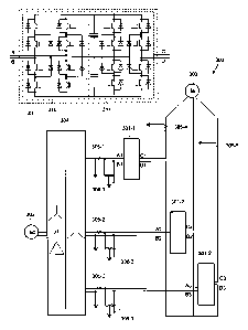
Fig. 5 is a schematic diagram of system 300, and further including an example
three-phase DC bus voltage combiner 501 and an example controller 502. In this
example, the three motor phases are labeled as u, v, and w. Controller 502 may
read
feedback signals from converter modules 310, inverter modules 311, and current
and
voltage sensing devices 305 and 306. Based on these feedback signals,
controller 502
may provide gate signals for dynamically controlling the on/off states of the
various
switching devices (e.g., transistors) in the converter and inverter modules
310 and 311.
Combiner 501 may receive, as inputs, the voltages of the various DC buses. In
this
example, the inputs to combiner 501 may be or otherwise depend on the voltages
across DC buses X1-Y1, X2-Y2 X3-Y3, Z1-Y1, Z2-Y2, and Z3-Y3, or a subset
thereof.
The output of combiner 501 may be one or more output voltages that depend upon
the
input voltages. In the present example, the output voltage from combiner 501
is labeled
as Vdc.
The output voltage Vdc of combiner 501 may depend on the input voltages in any
way desired. In some examples, voltage Vdc is or otherwise depends on the
average of
the input voltages. The average may be weighted or unweighted. For instance,
Vdc
may equal or otherwise depend on (X1+ Z1 + X2 + Z2 + X3 + Z3) / 6, where X1 is
shorthand for the voltage across DC bus X1-Y1; Z1 is shorthand for the voltage
across
7
CA 02745664 2011-07-07
DC bus Z1-Y1; X2 is shorthand for the voltage across DC bus X2-Y2; Z2 is
shorthand
for the voltage across DC bus Z2-Y2; X3 is shorthand for the voltage across DC
bus X3-
Y3; and Z3 is shorthand for the voltage across DC bus Z3-Y3. As another
example,
Vdc may equal C * (K1 *X1 + L1*Z1 + K2*X2 + L2*Z2 + K3*X3 + L3*Z3) / 6, where
each
of C, K1-K3, and L1-L3 is a predetermined constant of any value. The values of
C, K1-
K3, and L1-L3 may be equal to or different from each other, may each be less
than one,
equal to one, or greater than one, and may be positive or negative. Moreover,
the
combination (e.g., average) may be an instantaneous combination that takes
into
account only present values of the DC bus voltages, or it may be a combination
that
also takes into account past values of the DC bus voltages such as those
occurring
within a sliding time window. Thus, where a sliding window average is used,
Vdc may
be expressed as, e.g.:
1 n+T
- Z (K1(i)X 1(i) +L1(i)Z1(i) + K2(i)X2(i) + L2(i)Z2(i) + K3(i)X3(i) +
L3(i)Z3(i))
6T ,=n
where i is a time index value, n is the beginning value of index i of the
sliding window at
a given moment, and T is the width of the sliding window.
Combiner 501 and controller 502 may be implemented using dedicated circuitry
and/or a computer, and may be separate units from each other or embodied as a
single
integrated unit. Where a computer is used, the computer may execute software
to
perform the functions of combiner 501 and/or controller 502. For example, Fig.
6 is a
functional block diagram of an example computer 600 that may be used to
implement
combiner 501 and/or controller 502, which may include hardware that may
execute
software to perform specific functions. The software, if any, may be stored on
a
computer-readable medium 602 in the form of computer-readable instructions.
Computer 600 may read those computer-readable instructions, and in response
perform
various steps as defined by those computer-readable instructions. Thus, any
functions
attributed to the example combiner 501 and/or controller 502 as described
herein may
be implemented, for example, by reading and executing such computer-readable
8
CA 02745664 2011-07-07
instructions for performing those functions, and/or by any hardware subsystem
(e.g., a
processor 601) from which computer 600 is composed. Additionally or
alternatively, any
of the above-mentioned functions may be implemented by the hardware of
computer
600, with or without the execution of software. For example, computer 600 may
be or
include one or more microprocessors, central processing units (CPUs), and/or
other
types of circuitry configured to perform some or all of the functions
attributed to
computer 600. In such embodiments, processor 601 may be implemented as or
otherwise include the one or more microprocessors, CPUs, and/or other types of
circuitry.
A computer may include any electronic, electro-optical, and/or mechanical
device, or system of multiple physically separate or integrated such devices,
that is able
to process and manipulate information, such as in the form of data. Non-
limiting
examples of a computer include one or more personal computers (e.g., desktop,
tablet,
handheld, or laptop), mainframes, servers, and/or a system of these in any
combination
or subcombination. In addition, a given computer may be physically located
completely
in one location or may be distributed amongst a plurality of locations (i.e.,
may
implement distributive computing). A computer may be or include a general-
purpose
computer and/or a dedicated computer configured to perform only certain
limited
functions.
Computer-readable medium 602 may include not only a single physical
intransient medium or single type of such medium, but also a combination of
one or
more such media and/or types of such media. Examples of embodiments of
computer-
readable medium 602 include, but are not limited to, one or more memories,
hard
drives, optical discs (such as CDs or DVDs), magnetic discs, and magnetic tape
drives.
Computer-readable medium 602 may be physically part of, or otherwise
accessible by,
computer 600, and may store computer-readable instructions (e.g., software)
and/or
computer-readable data (i.e., information that may or may not be executable).
9
CA 02745664 2011-07-07
Computer 600 may also include a user input/output interface 603 for receiving
input from a user (e.g., via a keyboard, mouse, and/or remote control) and
providing
output to the user (e.g., via a display device, an audio speaker, and/or a
printer).
Computer 600 may further include an input/output interface 604 for physically
communicating signals (e.g., voltages, currents, and/or data) with devices
external to
computer 600. For example, the bus voltages may be input by input/output
interface
604 of combiner 501, and voltage Vdc may be output by input/output interface
604 of
combiner 501. Likewise, any inputs to controller 502 including voltage Vdc may
be
input by input/output interface 604 of controller 502, and any outputs from
controller 502
may be output by input/output interface 604 of controller 502.
Referring again to Fig. 5, controller 502 in this example may receive inputs
and
provide outputs as described below in Tables 1 and 2.
Table 1 - Inputs to Controller 502
signal description
Vul voltage measured between Al and
B1
Vvl voltage measured between A2 and
B2
Vw1 voltage measured between A3 and
B3
lul current measured through Al
lv1 current measured through A2
CA 02745664 2011-07-07
Iw1 current measured through A3
w2 measured or estimated angular
velocity of motor
w2* desired value of w2
Vdc output voltage of combiner 501
Vdc* desired value of Vdc
lu2 current measured through C1
Iw2 current measured through C3
Table 2 - Outputs From Controller 502
signal description
Vul* output voltage reference for module
310-1
Vv1 * output voltage reference for module
310-2
Vwl* output voltage reference for module
310-3
Vu2* output voltage reference for module
311-1
11
CA 02745664 2011-07-07
Vv2* output voltage reference for module
311-2
Vw2* output voltage reference for module
311-3
The operation of controllers that receive all of the inputs of Table 1 except
Vdc
and Vdc* are generally known, as are controllers that produce the outputs of
Table 2. In
this example, controller 502 is further configured to take into account inputs
Vdc and
Vdc*, as will be described in further detail with reference to Fig. 7.
Fig. 7 shows an example functional block diagram of controller 502. In this
example, controller 502 includes a voltage controller 701, a current
controller 702, a
three-to-two phase converter 703, a two-to-three phase converter 704, a phase-
locked
loop (PLL) circuit 705, an angular-velocity-to-angular-position converter 706
a speed
control circuit 707, a current controller 708, a three-to-two phase converter
709, an
angular-velocity-to-angular-position converter 710, and a two-to-three-phase
converter
711. Each of these elements 701-711 are individually well-known, and so
details of how
these elements operate need not be described herein.
As discussed previously, Vdc may represent a combination (e.g., an average) of
the DC bus voltages associated with the three motor phases. Voltage controller
701
compares Vdc with a desired, or target, value of Vdc, referred to as Vdc*, and
generates an internal signal Iq1*, representing a target torque current, as a
result of the
comparison.
Converter 703 receives signals lul, Iv1, and Iw1, which represent the actual
currents measured at the three phases, and converts them to the following two
phase
signals: actual torque current Iq1 and actual field current Id1. Also, PLL 705
generates
an internal signal w1 based on signals Vul, Vv1, and Vw1. Converter 706
generates
another internal signal, 01, which represents an angular position, based on
signal w1.
12
CA 02745664 2011-07-07
Signal Id1* as shown in Fig. 7 represents a target field current, and may be
set to
a fixed value, such as zero, and/or may be set by a target field current value
controller
712, such as a volt-ampere reactive (VAR) controller or a power factor
controller.
Current controller 702 receives the ld 1 *, lq 1 *, Iq 1, and Id l signals,
and based on these
received signals, outputs the following two internal signals: field voltage
reference Ed1
and torque voltage reference Eq1. Then, converter 704 generates the three
output
phase signals Vul*, Vvl*, and Vw1* based on Ed1, Eq1, and 91. Signals Vul*,
Vvl*,
and Vw1* indirectly control the on/off states of transistors of module 310 for
the
respective motor phases u, v, and w.
In parallel with the above processing, speed control 707 generates an internal
target torque current signal Iq2* based on signals w2 and w2*, which is fed
into current
controller 708. Converter 709 receives signals lu2 and W. Because the wye
point is
connected in the inverter side, signals Iu2 and Iw2 together represent all
three phases
of current, wherein the v-phase v current Iv is equal to -(Iu+lw). Converter
703 converts
Iu2 and lw2 to the following two phase signals: actual torque current Iq2 and
actual field
current Id2. This may provide the same result as having three current sensors
providing
the lu, Iv, and Iw currents. Also, converter 710 generates another internal
signal, 92,
which represents an angular position, based on signal w.
Target field current signal Id2* as shown in Fig. 7 may be set to a fixed
value,
such as that representing a no-load motor current, and/or may be set by target
field
current value controller 712. Current controller 707 receives the Iq2*, Id2*,
Iq2, and Id2
signals, and based on these received signals, outputs the following two
internal signals:
field voltage reference Ed2 and torque voltage reference Eq2. Then, converter
711
generates the three output phase signals Vu2*, Vv2*, and Vw2* based on Ed2,
Eq2,
and 02. Signals Vu2*, Vv2*, and Vw2* indirectly control the on/off states of
transistors
of module 311 for the respective motor phases u, v, and w.
As mentioned above, controller 502 provides some or all of signals Vul*, Vvl*,
Vwl*, Vu2*, Vv2*, and/or Vw2*, which control the various transistors of the
13
CA 02745664 2011-07-07
converter/inverter pairs 301. For example, each of signals Vul*, Vvl*, Vwl*,
Vu2*,
Vv2*, and Vw2* may be forwarded to a pulse-width modulation (PWM) controller
that
generates gate control pulses, based on these received signals, to control
each of the
individual transistors in modules 310 and 311. In particular, Vul*, Vvl*, and
Vwl* may
be used by the PWM controller to control the transistors of modules 310, and
Vu2*,
Vv2*, and Vw2* may be used by the PWM controller to control the transistors of
modules 311. In this way, motor 303 may be controlled based on the combined
(e.g.,
averaged) voltages of the DC buses associated with the three motor phases u,
v, and
w.
In previously-described embodiments, the motor has been shown by way of
example as a close-winding motor. However, an open-winding motor, which does
not
have a shared neutral point for all three phases, may alternatively be used.
For
example, Fig. 8 is a schematic diagram of an example motor drive system for
driving
such an open-winding motor 801. Because of the open-winding configuration,
input
transformer 304 may be entirely eliminated, if desired. And, in this
embodiment, three
motor current sensors 305-4, 305-5, 305-6 (one for each phase) are used,
because of
the possibility of a zero phase current. Moreover, this open-winding
configuration may
be used with or without a regenerative inverter for each phase. Combiner 501
and
controller 502 may also be used in the embodiment of Fig. 8.
Aspects as described herein may also be used in environments other than
controlling a motor. For example, Fig. 9 is a schematic diagram of an example
static
volt-ampere reactive (VAR) compensator that may be used to control the power
factor
of a system such as an industrial plant. In the example of Fig. 9, the VAR
compensator
includes a regenerative converter 901 for each phase, but without also
including an
inverter for each phase as in previous example embodiments. Again, combiner
501 and
controller 502 may also be used in the embodiment of Fig. 9.
Thus, various examples of an improved motor drive system and method have
been described. While certain embodiments of the present invention have been
14
CA 02745664 2011-07-07
described, these embodiments have been presented by way of example only, and
are
not intended to limit the scope of the inventions. Indeed, the novel methods
and
systems described herein may be embodied in a variety of other forms;
furthermore,
various omissions, substitutions and changes in the form of the methods and
systems
described herein may be made without departing from the spirit of the
inventions. For
example, while a three-phase system has been described, the invention may be
used in
connection with a multi-phase system having any number of phases, such as two,
three,
four, or more phases. The accompanying claims and their equivalents are
intended to
cover such forms or modifications as would fall within the scope and spirit of
the
inventions.