Note: Descriptions are shown in the official language in which they were submitted.
CA 02746817 2011-07-18
INPUT CONTROL APPARATUS AND METHOD WITH INRUSH CURRENT,
UNDER AND OVER VOLTAGE HANDLING
BACKGROUND
Technical Field
This disclosure is generally input control to handle input current,
and in particular to handle inrush current, and under voltage and over voltage
conditions. Such may, for example be useful in a wide variety of devices or
systems, particularly those with relatively large input capacitors, for
example
power converters, such as regulated switched mode power converters with bulk
input filter capacitors.
Description of the Related Art
Power converters are used to transform electrical energy, for
example converting between alternating current (AC) and direct current (DC),
adjusting (e.g., stepping up, stepping down) voltage or potential levels
and/or
frequency.
Power converters take a large variety of forms. One of the most
common forms is the switched-mode power converter or supply. Switched-
mode power converters employ a switching regulator to efficiently convert
voltage or current characteristics of electrical power. Switched-mode power
converters typically employ a storage component (e.g., inductor, transformer,
capacitor) and a switch that quickly switches between full ON and full OFF
states, minimizing losses. Voltage regulation may be achieved by varying the
ratio of ON to OFF time or duty cycle. Various topologies for switched-mode
power converters are well known in the art including non-isolated and isolated
topologies, for example boost converters, buck converters, synchronous buck
converters, buck-boost converters, and fly-back converters.
In the interest of efficiency, digital logic technology is employing
ever lower voltage logic levels. This requires power converters to deliver the
1
CA 02746817 2011-07-18
lower voltages at higher currents level. To meet this requirement, power
converters are employing more energy efficient designs. Power converters are
also increasingly being located in close proximity to the load in as point of
load
(POL) converters in a POL scheme. These power converters must generate
very low voltage levels (e.g., less than 1V) at increasingly higher current
levels
(e.g., greater than 10A). These relatively high current levels may be
difficult to
achieve with a single power converter.
Manufacturers are also increasingly employing POL schemes in
light of the widely varying voltage requirements in modern systems (e.g.,
computer systems). A POL scheme may be easier to design and/or fabricate,
take up less area, and/or produce less interference than employing multiple
different power buses. The POL schemes typically employ one or two power
buses with a number of POL regulators located close to specific components or
subsystems to be powered, for example microprocessors, field programmable
gate arrays (FPGAs), application specific integrated circuits (ASICs),
volatile
memory. The POL regulators adjust voltage to supply localized busses feeding
the specific components or subsystems.
Many devices employ input capacitors. For example, switched
mode power converters typically include a large internal bulk filter capacitor
to
filter the input power to reduce noise conducted out of the power converter
100,
back upstream to the source of the input power. The input capacitor may also
store and/or smooth input power.
However, upstream devices (e.g., power converters) may not be
able to source or start up devices with large capacitances. Often times,
upstream power converters are internally limited, and enter a "hiccup" mode or
repeatedly restart when faced with a large capacitive load. Thus, various
attempts have been made to design circuits which effectively limit inrush
current.
Present approaches to controlling the capacitive inrush current of
a device typically employ a series resistance or directly sensing the inrush
current of the device through resistive sensing, magnetic sensing, or Hall
effect
2
CA 02746817 2011-07-18
sensing. These approaches to sensing the actual input current waveform lead
to a substantial power loss, complicated designs, and/or high costs to address
electrical isolation requirements, as well as slow transient response. For
example, sensing an input current with a resistive element dissipates power
and requires specific circuitry to amplify the sense signal and reduce common
mode noise. Sensing with a magnetic element reduces power dissipation.
However, such an approach adds significant cost, requires added circuitry to
amplify the signal, and is only applicable in AC current sensing applications.
Thus, this approach is only useful for very high AC current applications. Due
to
their low sensitivity Hall effect sensors likewise require added circuitry to
amplify the signal and to reduce common mode noise.
Thus, the various approaches require a number of tradeoffs due
to design issues. For example, approaches which employ a permanently
placed resistor to limit inrush current suffer from a substantial decrease in
efficiency. It is typically difficult to derive an accurate input current
signal
without degrading the overall efficiency. Signal integrity degradation
resulting
from common mode noise/current is also a problem. Additionally, a voltage
shift of the signal down to the electrical circuit ground potential may occur
in
some designs. Further, many approaches have had difficulty in maintaining
fast transient response.
Additionally, many applications require that voltage be maintained
within an acceptable range. Thus, under voltage and over voltage conditions
must be monitored and handled.
New approaches to handling inrush current, under voltage and
over voltage monitoring are desirable.
BRIEF SUMMARY
Control circuits described herein may effectively accomplish
inrush current limiting. Such allows for predictable startup of a converter
from
bus sources that may themselves be current limited during the source startup.
Inrush current limiting also protects relatively large input or filter
capacitors from
3
CA 02746817 2011-07-18
damage at startup. Such may improve reliability for circuit designs that
require
a high capacitance density in order to meet stringent noise specifications.
Establishing a low and predictable inrush current can advantageously prevent
occurrence of power-on reset events or non-monotonic startup from a current-
limited or protected source.
The inrush current limiting may advantageously limit the inrush
current into a bulk capacitance of a device during the initial power up of a
device or during voltage transients without the need to directly sense the
input
current of the device. Instead, the inrush current limiting may be based on a
signal that is proportional to the input current of the device.
Such may be particularly useful in power converters that have a
large internal bulk filter capacitor. Power converter requirements continue to
evolve toward higher efficiency and minimizing the number external parts
needed. In the case of a switch mode power converter, incorporating bulk
capacitive filtering of the input power internal to the power converter
reduces
noise conducted out of the power converter back into the source.
Controlling the inrush current to a device (e.g., power converter)
capacitance reduces electrical stresses on the device, and on the any system
employing the device.
The approaches described herein may have a number of benefits
over existing approaches. For example, the approaches described herein may
effectively limit inrush current without directly sensing the input current,
resulting in overall higher efficiency. In particular, the approaches
described
herein may effectively limit inrush current based on a signal that is a mirror
or
representation of actual input current. The signal may advantageously be
inherently referenced to a ground return of the circuit, dramatically reducing
isolation requirements. By basing the inrush current control on a signal that
is
much smaller proportion of the actual inrush current, faster transient
response
to changes in the initial start up conditions or transient conditions can be
achieved. The approaches described herein can implement inrush current
limiting without an intrusive current measurement implementation, simplifying
4
CA 02746817 2011-07-18
the circuit design and reducing cost. The approaches described herein may
enable the reliable use of high-capacitance-density devices in the input
filter of
a power converter or other device. Further, the approaches described herein
may use common elements to accomplish four different functions: inrush
current limiting, under voltage lockout, remote enable, and over voltage
lockup,
using less complicated and less costly circuitry than prior approaches. Since
only a small current proportional to the total capacitive inrush current is
sensed
to monitor the total input current, higher efficiency, faster transient
response ,
lower circuit complexity and lower cost can be achieved than with existing
solutions. Lower parts count and lower cost result from the shared circuitry.
A
series switch or series pass device as the primary component to accomplish the
four functions allows for protection of downstream circuitry and monitoring a
state of the converter, whether delivering power or OFF. The approaches
described herein are not limited to power converters.
An input control circuit that controls inrush current may be
summarized as including a series switch electrically coupled in series on an
input line and operable in response to control signals to adjust a flow of an
input
current along the input line; a sense capacitor electrically coupled in
parallel
with an input filter capacitor between the input line and a ground reference
to
develop a signal that is proportional to the input current; a current sense
mirror
electrically coupled to the sense capacitor to receive the signal that is
proportional to the input current; and a clamp circuit responsive at least to
the
current sense mirror to provide the control signals to the series switch to
cause
the series switch to adjust the flow of the input current along the input
line. The
current sense mirror may include a first mirror transistor coupled to the
ground
reference through a first mirror resistor and a second mirror transistor
coupled
to the ground reference through a second mirror resistor R8, a base of the
first
mirror transistor and a base of the second mirror transistor commonly coupled
to the sense capacitor to maintain a constant inrush charge current to the
input
filter capacitor.
5
CA 02746817 2011-07-18
The input control circuit may further include a pair of trickle bias
resistors electrically coupled between the input line and a source of the
first
mirror transistor of the current sense mirror.
The input control circuit may further include an over voltage
lockout monitor circuit operable to detect an over voltage condition on the
input
line and coupled to supply a signal indicative of the over voltage condition
to the
clamp circuit, wherein the clamp circuit is further responsive at least to the
over
voltage lockout monitor circuit to provide control signals to the series
switch to
cause the series switch to stop the flow of the input current along the input
line.
The over voltage lockout monitor circuit may include a pair of over voltage
lockout resistors coupled as a voltage divider between the input line and the
ground reference via an over voltage lockout Zener diode which is coupled to
drive a switch controlling transistor which is in turn coupled to control the
series
switch.
The over voltage lockout monitor circuit may further includes a low
impedance charge path formed by a speedup diode and a speedup resistor
electrically coupled between the input line and the base of the transistor.
The input control circuit may further include an under voltage
lockout monitor circuit operable to detect an under voltage condition on the
input line and coupled to supply a signal indicative of the under voltage
condition to the clamp circuit, wherein the clamp circuit is further
responsive at
least to the under voltage lockout monitor circuit to provide control signals
to the
series switch to cause the series switch to stop the flow of the input current
along the input line. The under voltage lockout monitor circuit may include an
under voltage lockout comparator that has a first input and a second input,
the
first input coupled to the input line via a first under voltage lockout
resistor R5
and the second input coupled to a voltage reference source via a second under
voltage lockout resistor.
The input control circuit may further include an enable monitor
circuit operable in response to an enable single to provide control signals to
to
cause the series switch to stop the flow of the input current along the input
line.
6
CA 02746817 2011-07-18
The enable monitor circuit may be selectively operable electrically short the
first
and second inputs of the under voltage lockout comparator. The series switch
may be a P-Channel metal oxide semiconductor field effect transistor
(MOSFET) having a gate coupled to the clamp circuit and the clamp circuit
includes a switch controlling transistor coupled to control the series switch.
The input control circuit may further include an over voltage
lockout monitor circuit operable to detect an over voltage condition on the
input
line and coupled to supply a signal indicative of the over voltage condition
to the
clamp circuit; an under voltage lockout monitor circuit operable to detect an
under voltage condition on the input line and coupled to supply a signal
indicative of the under voltage condition to the clamp circuit; an enable
monitor
circuit operable in response to an enable single to provide control signals to
the
clamp circuit indicative of a disable state, and wherein the clamp circuit is
further responsive at least to the over voltage lockout monitor circuit, the
under
voltage lockout monitor circuit, and the enable monitor circuit to provide
control
signals to the series switch to cause the series switch to stop the flow of
the
input current along the input line in response to a signal indicative of the
over
voltage condition, the under voltage condition, or a disable state. The sense
capacitor may have a capacitance that is less than a capacitance of the input
filter capacitor
A method of operating an input control circuit may be summarized
as including capacitively producing a signal proportional to input current;
mirroring the signal proportional to input current; and adjusting a flow of
the
input current in response at least to the signal that is proportional to the
input
current to control an inrush current. Capacitively producing a signal
proportional to input current may include allowing a sense capacitor coupled
in
parallel with an input filter capacitor between an input line and a ground to
be
charged by the input current and adjusting a flow of the input current
includes
supplying a signal from a clamp circuit to a series pass device electrically
coupled in series on the input line.
7
CA 02746817 2011-07-18
The method may further include detecting at least one of an over
voltage condition or an under voltage condition on the input line; and in
response to detecting at least one of the over voltage condition or the under
voltage condition on the input line providing a signal to the clamp circuit
that
causes the series pass device to stop the flow of the input current.
The method may further include detecting an enable signal
indicative of a selected one of two states; in response to detecting the
enable
single of a first one of the two states providing a signal that causes the
series
pass device to stop the flow of the input current; and in response to
detecting
the enable single of a second one of the two states providing a signal that
causes an under voltage lockout monitor circuit to function.
An input control circuit operable to control inrush current may be
summarized as including a series switch operable in response to control
signals
to adjust a flow of an input current along an input line; an over voltage
lockout
monitor circuit operable to detect an over voltage condition on the input line
and
to produce a signal indicative of the over voltage condition; an under voltage
lockout monitor circuit operable to detect an under voltage condition on the
input line and to produce a signal indicative of the under voltage condition;
an
enable monitor circuit operable in response to an enable single to provide a
signal indicative of an enable/disable condition; and a clamp circuit that
provides control signals to control the series switch to adjust the flow of
the
input current along the input line in response to a signal that is
proportional to
the input current, and in response to the signals from the over voltage
lockout
monitor circuit, the under voltage lockout monitor circuit, and the enable
monitor
circuit. The clamp circuit may be responsive to the signals from the over
voltage lockout monitor circuit, the under voltage lockout monitor circuit,
and the
enable monitor circuit to provide control signals that cause the series switch
to
stop the flow of the input current along the input line.
The input control circuit may further include a sense capacitor
electrically coupled in parallel with an input filter capacitor between the
input
line and a ground reference to develop the signal that is proportional to the
8
CA 02746817 2011-07-18
input current; and a current sense mirror electrically coupled to the sense
capacitor to receive the signal that is proportional to the input current, the
clamp
circuit responsive to the current sense mirror.
BRIEF DESCRIPTION OF THE SEVERAL VIEWS OF THE DRAWINGS
In the drawings, identical reference numbers identify similar
elements or acts. The sizes and relative positions of elements in the drawings
are not necessarily drawn to scale. For example, the shapes of various
elements and angles are not drawn to scale, and some of these elements are
arbitrarily enlarged and positioned to improve drawing legibility. Further,
the
particular shapes of the elements as drawn, are not intended to convey any
information regarding the actual shape of the particular elements, and have
been solely selected for ease of recognition in the drawings.
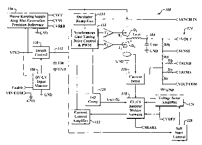
Figure 1 is a schematic diagram of a power converter including an
input control circuit with an inrush current control block, an over
voltage/under
voltage monitor block, and responsive to an enable signal, according to one
illustrated embodiment.
Figure 2 is a functional block diagram of the input control circuit of
Figure 1 to control a current flow on an input line, according to one
illustrated
embodiment.
Figure 3 is a detailed electrical schematic diagram of the input
control circuit of Figures 1 and 2, according to one illustrated embodiment.
Figure 4 is a flow diagram of a method of operating the input
control circuit of Figures 1-3, according to one illustrated embodiment.
Figure 5 is a flow diagram of a method of operating the input
control circuit of Figures 1-3, according to one illustrated embodiment, which
may be implemented as part of performing the method of Figure 4.
DETAILED DESCRIPTION
In the following description, certain specific details are set forth in
order to provide a thorough understanding of various disclosed embodiments.
9
CA 02746817 2011-07-18
However, one skilled in the relevant art will recognize that embodiments may
be
practiced without one or more of these specific details, or with other
methods,
components, materials, etc. In other instances, well-known structures
associated with power conversion topologies have not been shown or
described in detail to avoid unnecessarily obscuring descriptions of the
embodiments.
Unless the context requires otherwise, throughout the
specification and claims which follow, the word "comprise" and variations
thereof, such as, "comprises" and "comprising" are to be construed in an open,
inclusive sense, that is as "including, but not limited to."
Reference throughout this specification to "one embodiment" or
an embodiment" means that a particular feature, structure or characteristic
described in connection with the embodiment is included in at least one
embodiment. Thus, the appearances of the phrases "in one embodiment" or "in
an embodiment" in various places throughout this specification are not
necessarily all referring to the same embodiment. Furthermore, the particular
features, structures, or characteristics may be combined in any suitable
manner
in one or more embodiments.
As used in this specification and the appended claims, the
singular forms "a," "an," and "the" include plural referents unless the
content
clearly dictates otherwise. It should also be noted that the term "or" is
generally
employed in its sense including "and/or" unless the content clearly dictates
otherwise.
As used in the specification and the appended claims, references
are made to a "node" or "nodes." It is understood that a node may be a pad, a
pin, a junction, a connector, a wire, or any other point recognizable by one
of
ordinary skill in the art as being suitable for making an electrical
connection
within an integrated circuit, on a circuit board, in a chassis or the like.
The headings and Abstract of the Disclosure provided herein are
for convenience only and do not interpret the scope or meaning of the
embodiments.
CA 02746817 2011-07-18
Figure 1 shows a power converter 100, according to one
illustrated embodiment. The description of Figure 1 provides an overview of
the
structure and operation of the power converter 100, which structure and
operation are described in further detail with reference to Figures 2-7.
The power converter 100 may, for example, take the form of a
DC/DC power converter to convert (e.g., raise, lower) DC voltages. The power
converter 100 may, for example, include an output inductor Lout electrically
coupled to an output terminal +VOUT, a first active switch (i.e., high side
active
switch) T1 selectively operable to electrically couple the inductor Lout to a
voltage or potential input terminal VIN. A second device T2 electrically
couples
the output inductor Lout to a ground GND which is in turn electrically coupled
to
a ground or common input terminal VIN COM and a ground or common output
terminal VOUT COM.
As illustrated, the power converter 100 may advantageously take
the form of a synchronous buck converter, operable to lower a DC voltage or
potential. Where implemented as a synchronous buck converter, the second
device T2 takes the form of a second active switch (i.e., high side active
switch),
selectively operable to electrically couple the output inductor Lout to ground
GND. The power converter 100 may take forms other than a synchronous buck
converter, for example a buck converter where the second device takes the
form of a passive device, such as a diode (not shown).
The switches T1, T2 may take a variety of forms suitable for
handling expected currents, voltages and/or power. For example, the switches
T1, T2 make take the form of an active device, such as one or more metal oxide
semiconductor field effect transistors (MOSFETs). As illustrated in the
Figures,
the first or high side switch Ti may take the form of P-Channel MOSFET, while
the second or low side switch T2 make take the form of an N-Channel
MOSFET. The output inductor Lout may be coupled via a node 102 to the
drains DI, D2 of the MOSFET switches T1, T2 respectively. The power
converter 100 may employ other types of switches, for example insulated gate
bipolar transistors (IGBTs). While only one respective MOSFET is illustrated,
11
CA 02746817 2011-07-18
each of the first and/or second switches T1, T2 may include two or more
transistors electrically coupled in parallel.
The power converter 100 may include an output capacitor Cout
electrically coupled between ground GND and a node 104 between the output
inductor Lout and the output terminal +VOUT. Output capacitor Cout may
smooth the output supplied to the output terminal +VOUT.
On an input side, the power converter 100 may include an
auxiliary power supply and voltage reference generation block 106, an over
voltage/under voltage monitor block 108 and/or an "in rush" current control
block 110.
The auxiliary power supply and voltage reference generation
block 106 implements a house keeping supply generation function, amplifier
bias generation function and precision reference generation function,
resulting
in a positive supply voltage or potential VCC, a negative supply voltage or
potential or ground VSS, and a precision reference voltage VREF. The
structure and operation of the auxiliary power supply and voltage reference
generation block 106 can take any existing form, and is not a subject of this
application so is not described in further detail.
The over voltage/under voltage monitor block 108 monitors
instances of over voltage and/or under voltage conditions, supplying a control
signal via a control line (not called out in Figure 1) to the "in rush"
current
control block 110 as needed. The over voltage/under voltage monitor block 108
or other components may be triggered via an enable signal via an enable input
terminal ENABLE. The "inrush" current control block 110 controls "inrush"
current, directly limiting current to input capacitor(s) Cin, reducing
electrical
stresses on the power converter 100 and any system into which the power
converter 100 is incorporated. Power converters 100 typically employ large
internal bulk filter capacitors to filter the input power to reduce noise
conducted
out of the power converter 100, back upstream to the source of the input
power.
The input capacitor Gin is electrically coupled between ground GND and a node
111 between the "inrush" current control block 110 and the first active switch
T1.
12
CA 02746817 2011-07-18
The "inrush" current control block 110 is configured to control the "inrush"
current that flows to the input capacitor, particularly at initial application
of the
input voltage or potential VIN.
The structure and operation of the over voltage/under voltage
monitor block 108, the "inrush" current control block 110, and the input
capacitor(s) Cin may take any existing form, and are not subjects of this
application so are not described in further detail.
Control of the converter circuit (e.g., synchronous buck converter)
is realized via a number of components or assemblies, represented in Figures 1
and 2 as blocks.
The power converter 100 includes a synchronous gate timing
drive control and pulse width modulation (PWM) block 112. The synchronous
gate timing drive control and pulse width modulation block 112 generates gate
control signals to control the switches T1, T2, for example via amplifiers U1,
U2,
respectively. The synchronous gate timing drive control and pulse width
modulation block 112 may optionally receive a share signal via a share input
terminal SHARE from one or more other power converters, for example when
electrically coupled to a common load for current sharing operation. The
structure and operation of the a synchronous gate timing drive control and
pulse width modulation (PWM) block 112 can take any existing form, and is not
a subject of this application, so is not described in further detail.
The power converter 100 includes an oscillator ramp generation
block 114, also interchangeably referred to herein and in the claims as
oscillator
or oscillator circuit 114. The oscillator ramp generation block 114 generates
an
oscillating ramp signal and provides the oscillating ramp signal to the
synchronous gate timing drive control and pulse width modulation block 112.
Advantageously, the oscillator ramp generation block 114 may be selectively
synchronized to an external source over a wide frequency range. The oscillator
ramp generation block 114 may receive a synchronization signal via a
synchronization input terminal SYNC IN, to synchronize operation with one or
more other power converters or other devices or systems, for example a clock
13
CA 02746817 2011-07-18
of a system in which power converter 100 is installed. Such synchronization
may advantageously reduce overall system noise. The oscillator ramp
generation block 114 may advantageously take a form that provides for external
slope modulation of the ramp signal, a wider temperature range and/or an ultra
wide synchronous frequency range as compared to existing oscillator ramp
generation circuits. The oscillator ramp generation block 114 may
additionally,
or alternatively, take a form that advantageously employs less complex types
of
components and/or is less expensive to produce as compared to existing
oscillator ramp generation circuits. The structure and operation of exemplary
embodiments of the oscillator ramp generation block 114 are described in
detail
herein with reference to Figures 2-7.
At a high level, the power converter 100 utilizes an inner current
control loop and an outer voltage control loop. The inner current control loop
is
implemented via a current sense block 116, a current limiting/current sharing
(CUCS) resistor network 118, a 1-D (one minus duty cycle) compensation block
120 and a current control amplifier 122. The outer voltage control loop is
implemented by a voltage sense resistor divider network 124 (e.g., resistor
Rfb
coupled between voltage output terminal +VOUT and sense terminal SENSE,
divider resistors Rd, Rc, and trim resistors Rb, Ra coupled to trim terminals
TRIMB, TRIMA, respectively) and a voltage error amplifier 126 which feeds the
CUCS resistor network 118 to ultimately control the output voltage of the
power
converter 100.
With respect to the inner current control loop, the current sense
block 116 implements current sensing over a portion of a cycle of the power
converter 100, for example over the ON or CLOSED portion of one of the
switches T1, T2. The current sense block 116 provides a signal to the CL/CS
resistor divider network 118 to control the current control amplifier 122,
which
signal is indicative of the sensed current. For example, the current sense
block
116 may sense current over each portion of a cycle during which portion the
low side switch T2 is ON or CLOSED (i.e., conducting), electrically coupling
the
14
CA 02746817 2011-07-18
output inductor Lout to ground GND, while neglecting those portions of the
cycle
when the low side switch T2 is OFF or OPEN.
Where the output current of the synchronous buck converter
circuit in the power converter 100 is sensed at the low side switch (e.g.,
MOSFET synchronous switch) T2, the average of this sensed current is equal to
to*(1-D), where D is defined as the duty cycle of the high side switch (e.g.,
MOSFET) Ti. Since this signal is dependent on the duty cycle and negative in
value, a compensation signal that is a direct function of the duty cycle is
scaled
via the 1-D compensation block 120, and summed with the sensed current
signal by the CUCS resistor network 118. The resultant signal is optionally
level shifted in the CL/CS resistor network 118 to create a level shifted
compensated signal. The level shifted compensated signal may then be
averaged by the current control amplifier 122, and the averaged signal used to
control the output current of the power converter 100.
The current control amplifier 122 generates control signals based
at least on the level shifted compensated signals from the CUCS resistor
divider network 117 to control the synchronous gate timing drive control and
pulse width modulation block 112.
With respect to the inner current control loop, the voltage sense
resistor network 124 (e.g., resistor Rfb coupled between voltage output
terminal
+VOUT and sense terminal SENSE, divider resistors Rd, Rc, and trim resistors
Rb, Ra coupled to trim terminals TRIMB, TRIMA, respectively) senses voltage
or potential at the output terminal +VOUT with respect to the ground terminal
VOUTCOM. The voltage sense resistor network 124 supplies a signal
indicative of the sensed voltage or potential to the voltage sense amplifier
126.
The voltage sense amplifier 126 generates a voltage error signal which
indicates a difference between the sensed voltage or potential and a reference
voltage or potential. Hence, the voltage sense amplifier 126 is
interchangeably
referred to herein and in the claims as voltage error amplifier 126. The
voltage
error amplifier 126 provides the voltage error signal to the current control
amplifier 122 via the CUCS resistor divider network 118, for use in generating
CA 02746817 2011-07-18
the control signals supplied to the synchronous gate timing drive control and
pulse width modulation block 112 to control output voltage or potential of the
power converter 100.
The power converter 100 may optionally include a soft start
control block 128. The soft start control block 128 may receive the precision
voltage reference signal VREF from the auxiliary power supply and voltage
reference generation block 106. The soft start control block 128 may control
various soft start characteristics of the power converter 100, for example
soft-
start time, current limit thresholds, current limit on-time and output voltage
or
potential level at which control is handed over to a main control loop. The
soft
start control block 128 may, for example, provide a progressively increasing
pulse width, forming a startup voltage ramp which is proportional to a level
of a
supply voltage VCC, for instance without the need of an external capacitor.
The structure and operation of the soft start control block 128 can take any
existing form, and is not a subject of this application so is not described in
further detail.
The topology illustrated in and described with reference to Figure
1 is illustrative of only one of the many possible converter topologies which
may
employ the auxiliary power supply and voltage reference generation block 106
described herein. For example, the auxiliary power supply and voltage
reference generation block 106 may be employed in power converters which
use a different converter circuit topology, for instance boost converter, buck
converter or fly-back converter topologies. Also for example, the auxiliary
power supply and voltage reference generation block 106 may be employed in
power converters which use a different control topology, for instance a
control
topology that senses output current over an entire cycle of the waveform
without the need for compensation, or which senses current at the high side
active switch. Thus, this application, and in particular the claims, should
not be
limited to the specific topology illustrated in and discussed with reference
to
Figure 1 unless expressly stated therein.
16
CA 02746817 2011-07-18
Figure 2 shows an input control circuit 200 which implements both
the inrush control block 110 (Figure 1) and over voltage/under voltage monitor
block 108 (Figure 1) to control a current flow on an input line 202 between an
input pin, terminal or node, an output pin, terminal or node, and an input or
filter
capacitor or capacitance Cin (e.g., bulk filter capacitor), according to one
illustrated embodiment.
A primary function of the input control circuit 200 is control of an
inrush current that flows into the input capacitor or capacitance Cin at
initial
application of the input voltage or potential Vin, VIN COM, in order to
maintain a
defined current level. Secondary functions of the input control circuit 200
include implementing enable functionality, under voltage lockout (UVLO) and/or
over voltage lockout (OVLO) protection. The approaches described herein
advantageously employ a signal that is a mirror or representation of actual
input
current to assess, monitor or otherwise reflect the inrush current to the
input
capacitor or capacitance Cin and control the same. The approaches described
herein advantageously employ a signal that is inherently referenced to ground.
The input control circuit 200 implements inrush current control via
a switch Si, a sense capacitor Csense, a clamp circuit 208 and a current sense
mirror circuit 210.
The switch S, is electrically coupled in series in the input line 202
between the input pin, terminal or node 204 and the output pin, terminal or
node
206. Hence, the switch S, is interchangeably referred to herein and in the
claims as series switch or series pass device. The switch S, is operable in
response to control signals to adjust or regulate a flow of current
therethrough,
on the input line 202. For example, the switch S, is not only operable to stop
a
flow of current, but may also linearly regulate the flow of current. The
switch S,
may take a variety of forms, suitable for handling expected currents, voltages
or
power levels on the input line 202. For example, the switch S, may take the
form of a metal oxide semiconductor field effect transistor (MOSFET), for
instance a P-Channel MOSFET as illustrated in Figure 2.
17
CA 02746817 2011-07-18
The sense capacitor Csense is electrically coupled in parallel with
the input capacitor Cin, between the input line 202 and a ground reference
GND via the current sense mirror circuit 210. Thus, the same voltage appears
across the two capacitors Csense, Cin. Consequently, the current that charges
the sense capacitor Csense is proportional to the current that charges the
input
capacitor Cin. The charge current in either of the capacitors Csense, Cin can
be described by the fundamental relation:
I=C*dv/dt.
For each of the capacitors Csense, Cin, the fundamental current
(I) versus voltage (V) equation is:
I Csense=Csense*dv/dt
ICin=Cin*dv/dt.
Given that the change in voltage or potential with respect to time
(dv/dt) for the two capacitors Csense, Cin is the same, the relationship that
defines the proportionality constant between the charge currents of the two
capacitors Csense, Cin is:
lin=lsense *Cin/Csense.
From this relation it can be seen that the charge or inrush current
in the input capacitor Cin can be controlled by sensing and controlling the
charge current of the sense capacitor Csense. The ratio of capacitances of the
input capacitor Cin and sense capacitor Csense (i.e., Cin/Csense) may take on
a large variety of values, possibly with no minimum assuming low leakage
capacitors are employed. In this respect, it is noted that any leakage in the
sense capacitor Csense would form an error term, limiting the value of the
sense capacitor Csense. In an example, input capacitor Cin may have a
capacitance of about 220uF, while the sense capacitor Csense has a
capacitance of about 0.01 8uF; a difference of more than 4 decades. It is
further
noted that the ratio Cin/Csense could be limited in the current sense mirror
implementation illustrated in Figure 3.
18
CA 02746817 2011-07-18
The current sense mirror circuit 210 is coupled to the sense
capacitor Csense to sense the current in the sense capacitor Csense. The
current sense mirror circuit 210 mirrors or produces a signal that is
indicative of
or represents the sensed current.
The clamp circuit 208 is coupled to control the series switch Si.
For example, the clamp circuit 208 may be coupled to supply control signals to
a gate of the series switch S1. As is made clear below, the clamp circuit 208
is
responsive to signals from various components of the inrush control circuitry
110, including the sense current mirror 210. Thus, the clamp circuit 208 may
generate, produce or supply control signals to linearly regulate the flow of
current through the series switch S1 to maintain a constant value based on the
sensed current of the sense capacitor Csense.
The only prerequisite is that the series switch S, be ON or
CLOSED at the instant of application of the input voltage or potential Vin
(i.e.,
turn ON). This ensures sufficient initial charge current in the sense
capacitor
Csense to provide a feedback input into the current sense mirror circuit 210
to
start the inrush control process. Once sufficient current in the sense
capacitor
Csense is present, the startup sequence continues with the current sense
mirror circuit 210 controlling the clamp circuit 208 to continue holding a
voltage
or potential at a gate of the series switch S, at a level that maintains a
constant
inrush charge current to the input capacitor or capacitance Cin.
The input control circuit 200 optionally includes one or more of an
over voltage lockout(OVLO) monitor circuit 212 to implement OVLO monitoring
and control, Under voltage lockout (UVLO) monitor circuit 214 to implement
UVLO monitoring and control, and/or enable signal monitor circuit 216 to
implement enable signal monitoring and control. These circuits 212, 214, 216
may be coupled to the clamp circuit 208 to control the series switch S1.
The OVLO monitor circuit 212 is coupled to the input line 202 and
is operable to detect occurrences of over voltage conditions on the input line
202. Thus, the OVLO monitor circuit 212 may compare an actual voltage or
potential on the input line 202 to a threshold voltage or potential that is
19
CA 02746817 2011-07-18
indicative to an over voltage condition. In response to detection of an over
voltage condition, the OVLO monitor circuit 212 provides a signal to the clamp
circuit 208, to cause the clamp circuit 208 to cause the serial switch S, to
turn
OFF or OPEN, stopping the flow of current therethrough until the over voltage
condition can be remedied.
The UVLO monitor circuit 214 is coupled to the input line 202 via
an under voltage monitor resistor RI and is operable to detect occurrences of
over voltage conditions on the input line 202. The UVLO monitor circuit 214
may include a comparator U which compares the voltage or potential on the
input line 202 to a threshold voltage or potential VREF that is indicative to
an
under voltage condition. In response to detection of an under voltage
condition,
the UVLO monitor circuit 214 provides a signal to the clamp circuit 208, to
cause the clamp circuit 208 to cause the serial switch S, to turn OFF or OPEN,
stopping the flow of current therethrough until the under voltage condition
can
be remedied.
The enable signal monitor circuit 216 may receive an enable
signal Enable which is indicative of one of two states (e.g., HIGH, LOW) which
may be denominated respectively as enable and disable. The enable signal
monitor circuit 216 may apply the enable single to the clamp circuit 208, for
example via the comparator U. For example, the enable signal monitor circuit
216 may apply the enable signal to a positive or non inverting pin of the
comparator U. The state of the enable signal may be summed with the
threshold voltage or potential VREF. Thus, an output of the comparator U may
not trigger the clamp circuit 208 unless either: 1) the state of the enable
signal
is LOW (e.g., disable) or the input voltage or potential is below the
threshold
voltage or potential VREF (i.e., under voltage condition exists). As
illustrated,
the UVLO monitor circuit 214 and enable signal monitor circuit 216 may share
components (e.g., comparator U), and/or be combined as an Enable/UVLO
monitor circuit.
Thus, the clamp circuit 208 responds to three independent signal
inputs. The first input is from the Enable/ UVLO comparator U, which controls
CA 02746817 2011-07-18
the series switch S1 to turn ON power to the output 206 if the enable signal
Enable is true or HIGH and if the input voltage or potential VIN is above the
UVLO threshold for operation VREF. The second input is from the current
sense mirror circuit 210 which controls the series switch S1 to maintain a
constant input charge current to the input or filter capacitor or capacitance
Cin
as described above. The third input is from the OVLO monitor circuit 212 that
turns OFF the series switch S, at the instant the input voltage or potential
VIN
increases above a predetermined level to protect the powered output circuitry.
Figure 3 shows the input control circuit 200 of Figures 1 and 2 in
even more detail, operating to control a current flow on the input line 202
between the input pin, terminal or node 204 and the output pin, terminal or
node
206, and the input or filter capacitor or capacitance C1A, according to one
illustrated embodiment. As illustrated, the input control circuit 200 may
employ
less complex, and less costly discrete semiconductor components, chips
resistors and capacitors, than employed by existing control circuitry.
Inrush control
The inrush control function may be implemented by a series
switch such a series pass device or transistor Q1 (e.g., P- channel MOSFET), a
clamp circuit 208 including a switch controlling transistor Q4 (e.g., PNP
transistor) coupled to control a gate-to-source voltage of the series pass
device
or transistor Q1, a sense capacitor or capacitance C3 and a current sense
mirror circuit 210 to sense current or charge in the sense capacitor or
capacitance C3. As noted the series pass device or transistor Q1 is couple in
series in the input line 202 and operable to regulate current therethrough. A
gate of the series pass device or transistor Q1 is coupled to the input line
202
via a capacitor C4 and to a voltage or potential supply source VSS through a
supply resistor R9.
The clamp circuit 208 initiates a start up sequence turn ON of the
series pass device or transistor Q1 based on a state of the enable signal
Enable, and the UVLO and OVLO functions described below. Once series
21
CA 02746817 2011-07-18
pass device or transistor Q1 starts to turn ON, the sense capacitor or
capacitance C3 and input or filter capacitor or capacitance C1A start to
charge.
Any current passing through the sense capacitor or capacitance C3 will have to
pass through a first mirror transistor Q2 and a first mirror resistor RI 1
coupled
to a ground reference GND. Higher current through the first mirror resistor
R11
creates a larger voltage drop across the first mirror resistor R11, which is
reflected to a second mirror resistor R8, thus increasing current through a
second mirror transistor Q7. As current through the second mirror transistor
Q7
increases, a voltage drop across R14 becomes sufficient to turn ON the switch
controlling transistor Q4. The turning ON of the switch controlling transistor
Q4
starts the turning OFF of the series pass device or transistor Q1. The turning
OFF of series pass device or transistor Q1 adjusts (e.g., slows) the voltage
change (dv/dt) across the sense capacitor or capacitance C3, and thus reduces
the current change (di/dt) through the sense capacitor or capacitance C3 and
the input or filter capacitor or capacitance CiA. This negative feedback will
keep the series pass device or transistor Q1 operating in the linear region,
providing the desired voltage change (dv/dt) across the sense capacitor or
capacitance C3 to provide negative feedback to the current mirror controlling
the voltage change (dv/dt) across the sense capacitor or capacitance C3.
Since the sense capacitor or capacitance C3 and the input or filter capacitor
or
capacitance CIA are in parallel, control over the sense capacitor or
capacitance C3 will also control the voltage change (dv/dt) and thus the
current
change (di/dt) through the input or filter capacitor or capacitance C1A.
A pair of trickle bias resistors R10, R15 provide initial trickle bias
current for the mirror transistors Q2, Q7. A speedup diode CR4 and speedup
resistor R3 provide a low impedance charge path to speed up the turn ON of
the switch controlling transistor Q4. The speedup resistor R3 is typically a
factor of 10 to 100 times smaller in resistance value than the OVLO resistor
R14. OVLO resistors R12, R14 and Zener diode VR3 implement the OVLO
function as described below.
22
CA 02746817 2011-07-18
Over voltage Lockout
The OVLO threshold voltage or potential is set above the desired
operating voltage range of the powered circuitry. At an input voltage or
potential VIN above the normal operating voltage range but just below the
OVLO threshold, a base-emitter voltage of switch controlling transistor Q4
increases, slightly turning the switch controlling transistor Q4 ON, but not
hard
enough to short the gate of the series pass device or transistor Q1. Further
increases in the input voltage or potential VIN causes the current sense
mirror
circuit 210 to draw more current, and will cause the OVLO Zener diode VR3 to
conduct more. Both of these effects turn the switch controlling transistor Q4
ON harder. At the prescribed OVLO threshold, current through the OVLO
Zener diode VR3 will increase very rapidly, dropping more voltage across the
OVLO resistors R14, R12. Once the voltage across a first one of the OVLO
resistors R14 is around 0.65V, depending on temperature, the voltage will
cause the switch controlling transistor Q4 to turn ON, which will in cause the
series pass device or transistor Q1 to turn OFF, cutting off power to the
output
pin, terminal, or node 206. Reducing the input voltage or potential VIN down
to
within the normal operating voltage range reduces a voltage across the first
OVLO resistor R14, causing the switch controlling transistor Q4 to turn OFF,
and allowing the series pass device or transistor Q1 to turn ON, starting a
startup sequence.
Enable
The enable functionality or inhibit action is implemented via an
enable/ULVO transistor Q3, enable/ULVO operational amplifier U2B,
enable/ULVO resistors R4, R5, R7. With the enable pin or terminal 220 floating
or pulled HIGH, the enable/ULVO transistor Q3 is turned OFF setting a voltage
or potential at a negative input or pin of the enable/ULVO operational
amplifier
U2B equal to the input voltage or potential VIN. The voltage or potential at a
positive input or pin of the enable/ULVO operational amplifier U2B will be
equal
to the reference voltage or potential VREF (e.g., 2.5V). With the negative
input
23
CA 02746817 2011-07-18
or pin of the enable/ULVO operational amplifier U2B higher than the positive
input or pin thereof, the output of the enable/ULVO operational amplifier U2B
will be LOW and not affect the status of series pass device or transistor Q1.
The series pass device or transistor Q1 is then controlled by the UVLO
function
during power ON startup or by the OVLO function during an input voltage or
potential VIN over voltage condition.
Pulling the enable pin to LOW effectively ties the emitter of the
enable/ULVO transistor Q3 to ground, causing the enable/ULVO transistor Q3
to turn ON and saturate. With the enable/ULVO transistor Q3 saturated, its
collector voltage will be slightly lower than its base voltage. This causes an
output of the enable/ULVO operational amplifier U2B to go HIGH, providing
current through enable/ULVO diode CR3 to turn the mirror transistors Q2, Q7
ON hard enough to cause the switch controlling transistor Q4 to turn ON. With
the switch controlling transistor Q4 ON, the gate-to-source voltage of the
series
pass element or transistor Q1 is shorted, and the series pass element or
transistor Q1 will turn OFF, interrupting power flow.
Under voltage Lockout
The threshold VREF of the UVLO circuit 214 is set to be triggered
by an input voltage or potential VIN less than a desired operating voltage.
When the input voltage or potential VIN is at or below the UVLO threshold
VREF, the negative input or pin of the enable/ULVO operational amplifier U2B
will be at a lower voltage than the threshold VREF and lower than a voltage or
potential at the positive input or pin of the enable/ULVO operational
amplifier
U2B. This causes output of the enable/ULVO operational amplifier U2B to go
HIGH providing current through enable/ULVO diode CR3 to turn ON the mirror
transistors Q2, Q7 hard enough to cause the switch controlling transistor Q4
to
turn ON. With the switch controlling transistor Q4 ON, the gate-to-source of
the
series pass device or transistor Q1 is shorted, keeping the series pass device
or transistor Q1 OFF and interrupting power flow.
24
CA 02746817 2011-07-18
Increasing the input voltage or potential VIN to within a normal
operating input voltage range results in the negative input of the enable/ULVO
operational amplifier U2B at a higher voltage than the threshold VREF, the
voltage or potential at the positive input or pin of the enable/ULVO
operational
amplifier U2B. This causes the output of the enable/ULVO operational amplifier
U2B to go LOW causing the switch controlling transistor Q4 to turn OFF. With
the switch controlling transistor Q4 OFF, the voltage on the gate of the
series
pass device or transistor Q1 is pulled to negative supply voltage VSS, turning
on the series pass device or transistor Q1, and starting a startup sequence.
Operation of the above described circuit functions is predicated on
the presence of bias voltages or potentials, positive supply voltage or
potential
VCC and negative supply voltage or potential VSS at or below the UVLO
threshold VREF.
Figure 4 shows a flow diagram of a method 400 of operating the
input control circuit 110/108, 200 of Figures 1-3, according to one
illustrated
embodiment.
At 402, an input line 202 receives input current VIN at an input
terminal, pin or node 204. The input voltage or potential VIN may be the input
voltage supplied to the power converter 100 (Figure 1) from some upstream
component. For example, the input voltage or potential VIN may be supplied to
the power converter from a rectifier, a DC/DC converter, an isolating
converter
stage, and/or a DC electrical power storage device such as an array of
chemical battery cells or ultra-capacitors.
At 404, the sense capacitor Csense (Figure 2), C3 (Figure 3)
capacitively produces a signal proportional to input current by charging from
the
input current. At 406, a current sense mirror circuit mirrors the signal
proportional to input current.
At 408, a switch S1 (Figure 2), series pass device or transistor
(Figure 3) adjusts a flow of input current through the input line 202 in
response
at least to the signal that is proportional to the input current.
CA 02746817 2011-07-18
At 410, an OVLO monitor circuit 212 monitors for an over voltage
condition on the input line 202. At 412, the OVLO monitor circuit 212
determines If an over voltage condition occurred. If an over voltage condition
has occurred, then the OVLO monitor circuit provides a signal to a clamp
circuit
208 at 414 that causes the switch S1, series pass device or transistor Q1 to
stop a flow of input current through the input line 202. Control may then
return
to 402. If an over voltage condition has not occurred, control passes directly
to
416.
At 416, an UVLO monitor circuit 214 monitors for occurrence of an
under voltage condition on the input line 202. At 418, the UVLO monitor
circuit
214 determines whether an under voltage condition has occurred. If an under
voltage condition has occurred, then the UVLO monitor circuit 214 provides a
signal to the clamp circuit 208 at 420 that causes the switch S1, series pass
device or transistor Q1 to stop a flow of input current through the input line
202.
Control may then return to 402. If an under voltage condition has not
occurred,
control passes directly to 422.
At 422, an enable circuit 216 monitors an enable line ENABLE for
enable signals. At 424 the enable circuit 218, comparator U or operational
amplifier U2B determines If the enable signal indicates a disable state. If
the
enable signal indicates a disabled state, then at 426 the enable circuit 216,
comparator U or operational amplifier U2B provide a signal to the clamp
circuit
208 that causes the switch S1, series pass device or transistor Q1 to stop a
flow of current in the input line 202. Control may then return to 402.
At 428 the enable circuit 218, comparator U or operational
amplifier U2B determines If the enable signal indicates an enable state. If
the
enable signal indicates an enable state, then at 430 the enable circuit 216,
comparator U or operational amplifier U2B provides a signal to that causes the
under voltage lockout circuit 214 to function.
The method 400 may repeat while the power converter 100 is
operational, the oscillation circuit 114 continually generating, producing or
supplying the oscillation ramp signal VRAMP. Typically, most of these
26
CA 02746817 2011-07-18
operations or acts will be execute concurrently and fairly continuously by the
circuitry.
Figure 5 shows a method 500 of operating the input control circuit
110/108, 200 of Figures 1-3, according to one illustrated embodiment. The
method 500 may be implemented as part of performing the method 400 of
Figure 4.
At 502, a sense capacitor Csense coupled in parallel with an input
or filter capacitor or capacitance CIN, C3 between input line 202 and ground
GND to be charged by input current is allowed to charge by an input current
carried by the input line 202.
At 504, a signal is supplied from a clamp circuit 208 to a switch S1,
series pass device or transistor Q1 electrically coupled in series on input
line
202. The signal may cause the switch S1, series pass device or transistor Q1
to
turn ON, allow current to pass on the input line 202, or turn OFF and thereby
preventing input current from being supplied to the input or filter capacitor
or
capacitance CIN, C3.
While described above in the environment of a power converter,
and in particular a switch mode DC/DC synchronous buck power converter, the
control circuitry described herein may be advantageously employed in a large
variety of other environments. Such environments may include other types of
DC/DC power converters (e.g., boost, buck-boost, flyback), whether isolated or
non-isolated. Such may also include other types of power converters, including
inverters (DC/AC). Such may also include many other types of non-power
converter environments, which require inrush current control, OVLO protection,
UVLO protection, and remote enable functionality. Such may be particularly
useful for systems which have relatively large input or filter capacitors or
capacitance..
The specific values, such as specific voltages or potentials, used
herein are purely illustrative, and are not meant to be in anyway limiting on
the
scope. Likewise, the arrangements and topologies are merely illustrative and
other arrangements and topologies may be employed where consistent with the
27
CA 02746817 2011-07-18
teachings herein. While specific circuit structures are disclosed, other
arrangements that achieve similar functionality may be employed. The terms
switched mode and switch mode are used interchangeable herein and in the
claims.
The methods illustrated and described herein may include
additional acts and/or may omit some acts. The methods illustrated and
described herein may perform the acts in a different order. Some of the acts
may be performed sequentially, while some acts may be performed
concurrently with other acts. Some acts may be merged into a single act or
operation through the use of appropriate circuitry.
The various embodiments described above can be combined to
provide further embodiments. All of the U.S. patents, U.S. patent application
publications, U.S. patent applications, foreign patents, foreign patent
applications and non-patent publications referred to in this specification
and/or
listed in the Application Data Sheet, including but not limited to commonly
assigned U.S. patent applications:
Serial No. _/ , titled "POWER CONVERTER
APPARATUS AND METHOD WITH COMPENSATION FOR LIGHT LOAD
CONDITIONS" (Atty. Docket No. 480127.408);
Serial No. _/ , titled "SELF SYNCHRONIZING POWER
CONVERTER APPARATUS AND METHOD SUITABLE FOR AUXILIARY BIAS
FOR DYNAMIC LOAD APPLICATIONS" (Atty. Docket No. 480127.409);
Serial No. _/ , titled "POWER CONVERTER
APPARATUS AND METHOD WITH COMPENSATION FOR CURRENT
LIMIT/CURRENT SHARE OPERATION" (Atty. Docket No. 480127.411);
Serial No. _/ , titled "OSCILLATOR APPARATUS AND
METHOD WITH WIDE ADJUSTABLE FREQUENCY RANGE" (Atty. Docket
No. 480127.412); and
Serial No. titled "POWER CONVERTER
APPARATUS AND METHODS" (Atty. Docket No. 480127.413P1);
28
CA 02746817 2011-07-18
all filed on July 18, 2011, are incorporated herein by reference, in
their entirety. Aspects of the embodiments can be modified, if necessary to
employ concepts of the various patents, applications and publications to
provide yet further embodiments.
These and other changes can be made to the embodiments in
light of the above-detailed description. In general, in the following claims,
the
terms used should not be construed to limit the claims to the specific
embodiments disclosed in the specification and the claims, but should be
construed to include all possible embodiments along with the full scope of
equivalents to which such claims are entitled. Accordingly, the claims are not
limited by the disclosure.
29