Note: Descriptions are shown in the official language in which they were submitted.
CA 02748106 2012-12-21
IMAGING MEMBERS FOR INK-BASED DIGITAL PRINTING
COMPRISING STRUCTURED ORGANIC FILMS
BACKGROUND OF THE INVENTION
[0001] In electrophotography, electrophotographic imaging or
electrostatographic imaging, the surface of an electrophotographic plate,
drum, belt or
the like (imaging member or photoreceptor) containing a photoconductive
insulating
layer on a conductive layer is first uniformly electrostatically charged. The
imaging
member is then exposed to a pattern of activating electromagnetic radiation,
such as
light. The radiation selectively dissipates the charge on the illuminated
areas of the
photoconductive insulating layer while leaving behind an electrostatic latent
image on
the non-illuminated areas. This electrostatic latent image may then be
developed to
form a visible image by depositing finely divided electroscopic marking
particles on
the surface of the photoconductive insulating layer. The resulting visible
image may
then be transferred from the imaging member directly or indirectly (such as by
a
transfer or other member) to a print substrate, such as transparency or paper.
The
imaging process may be repeated many times with reusable imaging members.
CA 02748106 2011-08-05
[0003] An electrophotographic imaging member may be provided in a number
of forms. For example, the imaging member may be a homogeneous layer of a
single
material such as vitreous selenium or it may be a composite layer containing a
photoconductor and another material. In addition, the imaging member may be
layered. Current layered organic imaging members generally have at least a
substrate
layer and two active layers. These active layers generally include (1) a
charge
generating layer containing a light-absorbing material, and (2) a charge
transport layer
containing electron donor molecules. These layers can be in any order, and
sometimes can be combined in a single or mixed layer. The substrate layer may
be
formed from a conductive material. In addition, a conductive layer can be
formed on
a nonconductive substrate.
[0004] The charge generating layer is capable of photogenerating charge
and
injecting the photogenerated charge into the charge transport layer. For
example, U.S.
Patent No. 4,855,203 to Miyaka teaches charge generating layers comprising a
resin
dispersed pigment. Suitable pigments include photoconductive zinc oxide or
cadmium sulfide and organic pigments such as phthalocyanine type pigment, a
polycyclic quinone type pigment, a perylene pigment, an azo type pigment and a
quinacridone type pigment. Imaging members with perylene charge generating
pigments, particularly benzimidazole perylene, show superior performance with
extended life.
[0005] In the charge transport layer, the electron donor molecules may be
in a
polymer binder. In this case, the electron donor molecules provide hole or
charge
transport properties, while the electrically inactive polymer binder provides
mechanical properties. Alternatively, the charge transport layer can be made
from a
charge transporting polymer such as poly(N-vinylcarbazole), polysilylene or
polyether carbonate, wherein the charge transport properties are incorporated
into the
mechanically strong polymer.
[0006] Imaging members may also include a charge blocking layer and/or an
adhesive layer between the charge generating layer and the conductive layer.
In
addition, imaging members may contain protective overcoatings. Further,
imaging
members may include layers to provide special functions such as incoherent
reflection
2
CA 02748106 2011-08-05
of laser light, dot patterns and/or pictorial imaging or subbing layers to
provide
chemical sealing and/or a smooth coating surface.
100071 Generally, the above-described electrophotographic systems utilize
a
dry, powdered pigment material referred to as a toner. These systems generally
require that the substrate be charged, and that the toner be fused to the
substrate, often
by heating the substrate, after transferring the toner from the receptor
surface to the
substrate. There is, however, a desire for methods and systems for printing
with
different types of pigment materials and on a wider variety of substrates.
100081 For example, one common family of alternative pigment material are
liquid-based inks, such as used in ink-jet and other forms of printing well-
known
today. In many modern printing applications, the inks used are comprised of
charged
particles suspended in a solvent carrier.
100091 Such liquid ink-based printing systems are limited because they
require
relatively low viscosity inks. The viscosity of the ink affects the printing
throughput,
the function of transferring to and fusing the image on a substrate, the
internal
operations of the printing system, the cleaning of the printing system and so
forth.
Thus, these systems generally are limited to using inks with a viscosity of
for example
less than 100 centipoise (cp). However, there are many applications for which
a
higher viscosity ink is advantageous. For example, higher viscosity inks may
permit
the use of a wider variety of inks and substrates, reduced cost, etc.
100101 A number of printing techniques accommodate high viscosity inks.
Gravure printing is one example of a well-known printing technology that can
accommodate a relatively wider range of ink viscosities. According to this
technique,
an image carrier (most often a drum) is provided with a pattern of relatively
very
small recessed areas or cells. An ink is spread over the image carrier such
that ink is
retained in the cells, but not on the lands between the cells. An image-
receiving
substrate is brought into pressured contact with the ink-bearing plate or
drum. In this
type of printing, the ink wicks out of the cells and onto the substrate, where
it is dried,
thereby imparting a marking onto the substrate. Gravure printing can
accommodate
higher viscosity inks than current electrophotographic methods, but the image
is not
3
CA 02748106 2012-12-21
=
variable from printing to printing ¨ the gravure pattern is a permanent part
of the
image carrier.
[0011] In such printing techniques that accommodate high
viscosity inks, ink
may be metered into an anilox, or gravure, roller such that the cells, or
grooves, are
partially filled. To form an image, the ink may be electrostatically pulled
out of the
cells in an image-wise fashion. Typically, metering rollers are used to meter
the
amount of ink applied to an anilox roller. An anilox roller may include a
cylindrical
surface with millions of very fine hollows, shaped as cells or grooves. Anilox
and
gravure are terms both referring to cylinders with small cells/ grooves on the
surface
and may be used interchangeably. Technically, the term anilox is used more in
flexographic printing and gravure is used in gravure printing. The gravure
cells may
usually be patterned in an image while the analox cells may not be. Ink to be
metered
is filled in the cells. Doctor blades or wiping blades are usually used to
clean the
lands of the anilox roller. In doctor blade mode, doctor blades may be placed
in an
angle more than 90 degrees with respect to the blade moving direction. In
wiping
blade mode, wiping blades may be placed in angles less than 90 degrees with
respect
to the blade moving direction.
[0012] Existing technologies for electrostatic printing
using anilox rollers
have a number of drawbacks. Traditional cleaning using doctor blades may leave
the
cells full which leads to the problem of high background printing. The blades
may be
adjusted, but blades have inherent problems, including particle trapping, non-
uniformity, speed limitations and cell pattern restrictions. For example, in a
single
blade system, there is an inherent conflict between the metering and cleaning
requirements of the blade, as it needs to be soft enough to go into the cells
or grooves,
but hard or stiff enough to effectively wipe off residue ink from the lands.
Another
technique used a wiping blade mode, but this mode works only at slow speeds,
as
higher speeds increase the hydrodynamic pressure significantly.
[0013] Efforts to combine the above-mentioned different
printing technologies
include, for example, WO 91/15813 (Swidlery), which discloses an electrostatic
image transfer system by which the negative or reverse of a desired image is
first
4
CA 02748106 2013-02-19
exposed onto the surface of a photoreceptor, then that image is transferred to
a toner
roller, where the image is reversed to create the desired image on the toner
roller.
This image on the toner roller may then be transferred to a substrate and
fused.
[0014] In U.S. Patent No. 3,801,315, a gravure member is used to form an
image on a substrate. The gravure member includes a number of evenly spaced
cells
with interstitial surface lands. A photoconductor is formed on the surface
lands only
(i.e., no photoconductive material within the cells). Pigment material is
deposited
within the cells. The photoconductor is exposed to an image, and in the
regions of
exposure the charge on the photoconductor is dissipated. In cells adjacent
charged
lands, the pigment material forms a concave meniscus, and in cells adjacent
discharged lands the pigment material forms a convex meniscus, due to the
electric
field effects on the surface tension of the pigment material. The image is
then
transferred from the gravure member to a conductively backed image-receiving
web
brought into contact with the gravure member. Where there is a conductive
difference
between land and conductive backing, and the pigment material is convex within
a
cell, the pigment material in the cell is transferred to the receiving web.
Where the
meniscus of the pigment material is concave within a cell and there is no
conductive
difference between land and web backing, no pigment material is transferred.
The
image may then be transferred from the web to a substrate. However, due to the
meniscus effects, and the fact that electrostatics are required to pull the
pigment
material out of the cells and onto the receiving web, the pigment material
must be of a
relatively low viscosity. Furthermore, the reference teaches using a separate
photoreceptor and gravure member, requiring cleaning of the ink off of the
photoreceptor for every printing pass.
(0015] Another application of electrophotography to a gravure-like
process is
disclosed in U.S. Patent No. 4,493,550. According to this reference, pigment
material
is disposed in cells and provided with a negative charge. A positively charged
photoreceptor is image-wise exposed such that certain regions are discharged
and
others retain the positive charge. The photoreceptor and the pigment
containing cells
CA 02748106 2011-08-05
, .
are brought proximate one another such that the opposite charge therebetween
causes
the pigment material to transfer from the cells to the photoreceptor where the
photoreceptor retains the positive charge but not where it is discharged. The
pigment
on the photoreceptor may then be transferred to substrate. Again, however, the
pigment material must be of a relatively low viscosity for the electrostatic
force to be
sufficient to pull the pigment material from the cell to the photoreceptor.
This
reference also teaches using a separate photoreceptor and gravure member,
requiring
cleaning of the ink off of the photoreceptor for every printing pass, leading
to
degradation problems.
[0016] As more advanced, higher speed electrophotographic
copiers,
duplicators and printers have been developed, and as the use of such devices
increases
in both the home and business environments, degradation of image quality has
been
encountered during extended cycling. This repetitive cycling leads to a
gradual
deterioration in the mechanical and electrical characteristics. Moreover,
complex,
highly sophisticated duplicating and printing systems operating at very high
speeds
have placed stringent requirements upon component parts, including such
constraints
as narrow operating limits on the photoreceptors. For example, the numerous
layers
found in many modern photoconductive imaging members must be highly flexible,
adhere well to adjacent layers, and exhibit predictable electrical
characteristics within
narrow operating limits to provide excellent toner images over many thousands
of
cycles. One type of multilayered photoreceptor that has been employed for use
as a
belt or as a roller in electrophotographic imaging systems comprises a
substrate, a
conductive layer, a blocking layer, an adhesive layer, a charge generating
layer, a
charge transport layer and a conductive ground strip layer adjacent to one
edge of the
imaging layers. This photoreceptor may also comprise additional layers such as
an
anti-curl back coating and an optional overcoating layer.
[0017] Imaging members are generally exposed to repetitive
electrophotographic cycling, which subjects the exposed charge transport layer
thereof to abrasion, chemical attack, heat and multiple exposures to light.
This
repetitive cycling leads to a gradual deterioration in the mechanical and
electrical
characteristics of the exposed charge transport layer. Attempts have been made
to
6
CA 02748106 2012-12-21
overcome these problems. However, the solution of one problem often leads to
additional problems.
[0018] For example, other image member systems are also known to suffer
from a gradual deterioration in the mechanical and electrical characteristics
of the
exposed regions. For example, U.S. Patent Nos. 2,324,550 and 4,078,927
disclose
lithographic ink systems, and U.S. Patent No. 3,801,315 to Grundlach et al.
discloses
a gravure ink system that suffer from a gradual deterioration in the image
transfer
region.
[0019] An improved system and method to perform variable data printing of
viscous inks would permit digital production printing in, among other fields,
the
commercial graphic arts and packaging markets. The ability to use viscous
liquid inks
would provide numerous advantages, including use of higher density/viscosity
pigment, lower fixing energy (no fusing), larger substrate latitude, and lower
ink
spreading or dot gain.
[0020] Although known processes and materials are suitable for their
intended
purposes, a need remains for improved imaging members and processes employing
improved imaging members. For example, there remains a need in the art for
longer-
lasting imaging members. Such improved imaging member designs should include
increased wear resistance, i.e., low photoreceptor wear, while still providing
improved
toner transfer, improved cleaning properties, lower toner adhesion, and the
like.
There is also a need for imaging members that possess acceptable thermal
stability,
excellent chemical stability, and also have physical and mechanical stability.
There is
also a need for improved imaging members that may be utilized in dry (or
liquid)
xerographic imaging and printing systems and processes. Chemical stability as
mentioned herein refers, for example, to resistance attack from both dry and
liquid
toners and developers, view of the contact of the transfer element with
liquid, charge
additive, charge directors, toner resins, and pigments.
7
CA 02748106 2012-12-21
SUMMARY OF THE DISCLOSURE
[0021] The present disclosure addresses these and other needs by
providing an
imaging member for digital printing comprising: a substrate; a charge
generating
layer; an optional charge transport layer; and an outermost layer; wherein the
outermost layer comprises a structured organic film (SOF) comprising a
plurality of
segments, a plurality of linkers arranged as a covalent organic framework
(COF).
[0022] The present disclosure also provides an imaging member for digital
printing comprising: a substrate, a charge generating layer, and a charge
transport
layer, wherein an external layer of said imaging member comprises a SOF.
[0023] The present disclosure also provides a method for making such an
imaging member and a method of forming an image or printing with such an
imaging
member.
[0023a] In accordance with another aspect, there is provided an imaging
member for ink-based digital printing comprising:
a substrate;
a charge generating layer;
a charge transport layer; and
an optional overcoat layer;
wherein an outermost layer of the imaging member is an imaging surface that
comprises a structured organic film (SOF) comprising a plurality of segments
including at least a first segment type and a plurality of linkers including
at least a
first linker type arranged as a covalent organic framework (COF), wherein the
first
segment type and/or the first linker type comprises at least one atom that is
not
carbon.
10023b1 In accordance with a further aspect, there is provided an imaging
apparatus for ink-based digital printing, comprising:
an imaging member, wherein an outermost layer of the imaging member
comprises a structured organic film (SOF) comprising a plurality of segments
including at least a first segment type and a plurality of linkers including
at least a
first linker type arranged as a covalent organic framework (COF), wherein the
first
8
CA 02748106 2012-12-21
segment type and/or the first linker type comprises at least one atom that is
not
carbon;
a charging unit to impart an electrostatic charge on the imaging member;
an exposure unit to create an electrostatic latent image on the imaging
member;
an ink delivery unit to create an ink image on the imaging member;
a transfer unit to transfer the ink image from the imaging member; and
an optional cleaning unit.
[0023c] In accordance with another aspect, there is provided an imaging
member for ink-based digital printing comprising:
a substrate;
a charge generating layer;
a charge transport layer; and
an optional overcoat layer;
wherein an outermost layer of the imaging member is an imaging surface that
comprises a structured organic film (SOF) comprising a plurality of segments
including at least a first segment type and a plurality of linkers including
at least a
first linker type arranged as a covalent organic framework (COF), wherein the
SOF is
a substantially defect-free film, and the first segment type and/or the first
linker type
comprises a hydrogen.
BRIEF DESCRIPTION OF THE DRAWINGS
[0024] Other aspects of the present disclosure will become apparent as
the
following description proceeds and upon reference to the following figures
which
represent illustrative embodiments:
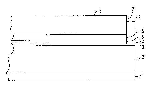
[0025] FIG. 1 represents a simplified side view of an exemplary
photoreceptor
that incorporates a SOF of the present disclosure.
[0026] FIG. 2 represents a simplified side view of a second exemplary
photoreceptor that incorporates a SOF of the present disclosure.
[0027] FIG. 3 represents a simplified side view of a third exemplary
photoreceptor that incorporates a SOF of the present disclosure.
8a
CA 02748106 2012-12-21
[0028] FIG. 4 is
a graphic representation that compares the Fourier transform
infrared spectral of the products of control experiments mixtures, wherein
only
N4,N4,N4',N4'-tetrakis(4-(methoxymethyl)phenyl)bipheny1-4,4'-diamine is added
to
the liquid reaction mixture (top), wherein only benzene-1,4-dimethanol is
added to the
liquid reaction mixture (middle), and wherein the necessary components needed
to
form a patterned Type 2 SOF are included into the liquid reaction mixture
(bottom).
8b
CA 02748106 2011-08-05
[0029] FIG. 5 is a graphic representation of a Fourier transform infrared
spectrum of a free standing SOF comprising N4,N4,N4',N4'-tetra-p-tolylbipheny1-
4,4'-diamine segments, p-xylyl segments, and ether linkers.
[0030] FIG. 6 is a graphic representation of a Fourier transform infrared
spectrum of a free standing SOF comprising N4,N4,N4',N41-tetra-p-tolylbipheny1-
4,4'-diamine segments, n-hexyl segments, and ether linkers.
[0031] FIG. 7 is a graphic representation of a Fourier transform infrared
spectrum of a free standing SOF comprising N4,N4,N4',N4'-tetra-p-tolylbipheny1-
4,4'-diamine segments, 4,4'-(cyclohexane-1,1-diy1)diphenyl, and ether linkers.
[0032] FIG. 8 is a graphic representation of a Fourier transform infrared
spectrum of a free standing SOF comprising of triphenylamine segments and
ether
linkers.
[0033] FIG. 9 is a graphic representation of a Fourier transform infrared
spectrum of a free standing SOF comprising triphenylamine segments, benzene
segments, and imine linkers.
[0034] FIG. 10. is a graphic representation of a Fourier transform
infrared
spectrum of a free standing SOF comprising triphenylamine segments, and imine
linkers.
[0035] FIG. 11 is a graphic representation of a photo-induced discharge
curve
(PIDC) illustrating the photoconductivity of a Type 1 structured organic film
overcoat
layer.
[0036] FIG. 12 is a graphic representation of a photo-induced discharge
curve
(PIDC) illustrating the photoconductivity of a Type 1 structured organic film
overcoat
layer containing wax additives.
[0037] FIG. 13 is a graphic representation of a photo-induced discharge
curve
(PIDC) illustrating the photoconductivity of a Type 2 structured organic film
overcoat
layer.
[0038] FIG. 14 is a graphic representation of two-dimensional X-ray
scattering data for the SOFs produced in Examples 26 and 54.
9
CA 02748106 2011-08-05
[0039] FIG. 15 is a graphic representation of a photo-induced discharge
curve
(PIDC) illustrating the photoconductivity of a various overcoat layers.
[0040] FIG. 16 is a graphic representation of cycling data that was
acquired
for various SOF overcoat layers.
[0041] Unless otherwise noted, the same reference numeral in different
Figures refers to the same or similar feature.
[0042] DETAILED DESCRIPTION
[0043] This disclosure is generally directed to imaging members,
photoreceptors, photoconductors, and the like, which comprise structured
organic
films (SOFs), such as in the imaging surface thereof, for digital printing
applications.
More specifically, the present disclosure is directed to rigid or drum
photoconductors,
and to single or multilayered flexible, belt imaging members, or devices
comprised of
an optional supporting medium like a substrate, a photogenerating layer, a
charge
transport layer, and a polymer coating layer, an optional adhesive layer, and
an
optional hole blocking or undercoat layer that comprise SOFs. The imaging
members, photoreceptors, and photoconductors illustrated herein (or imaging
surfaces
thereof), in embodiments, exhibit no or substantially no physical damage after
about
24 hours or more, such as greater than about 48 hours, such as about 72 hours
or
more, such as about 96 hours, or about 144 hours, of continuous exposure to
the ink
(the term "physical damage" refers for example damage, which optionally may be
visually detected, such as cracking, crazing, crystallization, phase
separation and
extraction; the term "substantially no physical damage" refers to less than 2%
of the
surface exhibiting physical damage, such as less than 1% of the surface
exhibiting
physical damage) have excellent wear resistance; extended lifetimes; provide
for the
elimination or minimization of imaging member scratches on the surface layer
or
layers of the member (imaging surface(s)), and which scratches can result in
undesirable print failures where, for example, the scratches are visible on
the final
prints generated; permit excellent electrical properties; minimum cycle up
after
extended electrical cycling; increased resistance to running deletion; solvent
resistance; and mechanical robustness. Additionally, in embodiments the
imaging or
CA 02748106 2011-08-05
photoconductive members (and/or imaging surfaces thereof) disclosed herein
possess
excellent, and in a number of instances low V, (residual potential), and the
substantial
prevention of V, cycle up when appropriate; high sensitivity; low acceptable
image
ghosting characteristics; and desirable toner cleanability.
[0044] Incorporating a structured organic film in the imaging member,
such as
in the charge transport layer, or other external layer of the imaging member,
such as
the imaging surface, may provide benefits such as decreased ink or toner
adhesion and
resultant less aggressive cleaning, improved transfer, and increased wear
resistance.
[0045] In embodiments, the imaging member is an intermediate transfer
belt,
sheet, roller, or film useful in xerographic, including digital, apparatuses.
However,
the imaging members herein comprising a SOF may be useful as belts, rollers,
drelts
(a drum/belt hybrid), and the like, for many different processes and
components such
as photoreceptors, fusing members, transfix members, bias transfer members,
bias
charging members, developer members, image bearing members, conveyor members,
cleaning members, and other members for contact electrostatic printing
applications,
xerographic applications, including digital, and the like. Further, the
imaging
members, herein, can be used for both liquid and dry powder xerographic
architectures.
[0046] The SOF overcoated photoreceptors exhibit increased mechanical
robustness that also allows more pressure to be used for applications like
electrostatic
proximity printing (SLIC), which relies on the photoreceptor being in physical
contact
with a metal or ceramic gravure roller. The increased pressure is one way to
help
make the development nip conditions more uniform, and enable more uniform
prints.
In embodiments, the pressure may be increased at least about 2 times, such as
about 4
times, the pressure generally applied using a belt in tension, or thick foam
underneath
the photoreceptor.
[0047] Also included within the scope of the present disclosure methods
of
imaging and printing with the imaging members illustrated herein.
[0048] As used herein, the term "ink-based digital printing" refers to,
for
example, a wide number of printing techniques, such as gravure, flexography,
and
11
CA 02748106 2011-08-05
. .
offset printing, which may accommodate a wide variety of inks. For example,
such
inks may include liquid inks with a viscosity greater than about 100 cp, such
as a
liquid ink with a viscosity from about 100 cp to about 200,000 cp.
[0049] In this specification and the claims that follow,
singular forms such as
"a," "an," and "the" include plural forms unless the content clearly dictates
otherwise.
[0050] The term "SOF" generally refers to a covalent organic
framework
(COF) that is a film at a macroscopic level. The phrase "macroscopic level"
refers,
for example, to the naked eye view of the present SOFs. Although COFs are a
network at the "microscopic level" or "molecular level" (requiring use of
powerful
magnifying equipment or as assessed using scattering methods), the present SOF
is
fundamentally different at the "macroscopic level" because the film is for
instance
orders of magnitude larger in coverage than a microscopic level COF network.
SOFs
described herein have macroscopic morphologies much different than typical
COFs
previously synthesized.
[0051] Additionally, when a capping unit is introduced into the
SOF, the SOF
framework is locally 'interrupted' where the capping units are present. These
SOF
compositions are `covalently doped' because a foreign molecule is bonded to
the SOF
framework when capping units are present. Capped SOF compositions may alter
the
properties of SOFs without changing constituent building blocks. For example,
the
mechanical and physical properties of the capped SOF where the SOF framework
is
interrupted may differ from that of an uncapped SOF.
[0052] The SOFs of the present disclosure are at the
macroscopic level
substantially pinhole-free SOFs or pinhole-free SOFs having continuous
covalent
organic frameworks that can extend over larger length scales such as for
instance
much greater than a millimeter to lengths such as a meter and, in theory, as
much as
hundreds of meters. It will also be appreciated that SOFs tend to have large
aspect
ratios where typically two dimensions of a SOF will be much larger than the
third.
SOFs have markedly fewer macroscopic edges and disconnected external surfaces
than a collection of COF particles.
12
CA 02748106 2011-08-05
[0053] In embodiments, a "substantially pinhole-free SOF" or "pinhole-
free
SOF" may be formed from a reaction mixture deposited on the surface of an
underlying substrate. The term "substantially pinhole-free SOF" refers, for
example,
to an SOF that may or may not be removed from the underlying substrate on
which it
was formed and contains substantially no pinholes, pores or gaps greater than
the
distance between the cores of two adjacent segments per square cm; such as,
for
example, less than 10 pinholes, pores or gaps greater than about 250
nanometers in
diameter per cm2, or less than 5 pinholes, pores or gaps greater than about
100
nanometers in diameter per cm2. The term "pinhole-free SOF" refers, for
example, to
an SOF that may or may not be removed from the underlying substrate on which
it
was formed and contains no pinholes, pores or gaps greater than the distance
between
the cores of two adjacent segments per micron2, such as no pinholes, pores or
gaps
greater than about 500 Angstroms in diameter per micron2, or no pinholes,
pores or
gaps greater than about 250 Angstroms in diameter per micron2, or no pinholes,
pores
or gaps greater than about 100 Angstroms in diameter per micron2.
[0054] In embodiments, the SOF comprises at least one atom of an element
that is not carbon, such at least one atom selected from the group consisting
of
hydrogen, oxygen, nitrogen, silicon, phosphorous, selenium, fluorine, boron,
and
sulfur. In further embodiments, the SOF is a boroxine-, borazine-,
borosilicate-, and
boronate ester-free SOF.
[0055] Molecular Building Block
[0056] The SOFs of the present disclosure comprise molecular building
blocks having a segment (S) and functional groups (Fg). Molecular building
blocks
require at least two functional groups (x 2) and may comprise a single type or
two
or more types of functional groups. Functional groups are the reactive
chemical
moieties of molecular building blocks that participate in a chemical reaction
to link
together segments during the SOF forming process. A segment is the portion of
the
molecular building block that supports functional groups and comprises all
atoms that
are not associated with functional groups. Further, the composition of a
molecular
building block segment remains unchanged after SOF formation.
13
CA 02748106 2011-08-05
[0057] Functional Group
[0058] Functional groups are the reactive chemical moieties of molecular
building
blocks that participate in a chemical reaction to link together segments
during the
SOF forming process. Functional groups may be composed of a single atom, or
functional groups may be composed of more than one atom. The atomic
compositions of functional groups are those compositions normally associated
with
reactive moieties in chemical compounds. Non-limiting examples of functional
groups include halogens, alcohols, ethers, ketones, carboxylic acids, esters,
carbonates, amines, amides, imines, ureas, aldehydes, isocyanates, tosylates,
alkenes,
alkynes and the like.
[0059] Molecular building blocks contain a plurality of chemical moieties, but
only a
subset of these chemical moieties are intended to be functional groups during
the SOF
forming process. Whether or not a chemical moiety is considered a functional
group
depends on the reaction conditions selected for the SOF forming process.
Functional
groups (Fg) denote a chemical moiety that is a reactive moiety, that is, a
functional
group during the SOF forming process.
[0060] In the SOF forming process the composition of a functional group
will
be altered through the loss of atoms, the gain of atoms, or both the loss and
the gain of
atoms; or, the functional group may be lost altogether. In the SOF, atoms
previously
associated with functional groups become associated with linker groups, which
are the
chemical moieties that join together segments. Functional groups have
characteristic
chemistries and those of ordinary skill in the art can generally recognize in
the present
molecular building blocks the atom(s) that constitute functional group(s). It
should be
noted that an atom or grouping of atoms that are identified as part of the
molecular
building block functional group may be preserved in the linker group of the
SOF.
Linker groups are described below.
[0061] Capping Unit
[0062] Capping units of the present disclosure are molecules that
'interrupt'
the regular network of covalently bonded building blocks normally present in
an SOF.
Capped SOF compositions are tunable materials whose properties can be varied
14
CA 02748106 2012-12-21
through the type and amount of capping unit introduced. Capping units may
comprise
a single type or two or more types of functional groups and/or chemical
moieties.
[0063] In embodiments, the capping units have a structure that is
unrelated to
the structure of any of the molecular building blocks that are added into the
SOF
formulation, which (after film formation) ultimately becomes the SOF.
[0064] In embodiments, the capping units have a structure that
substantially
corresponds to the structure of one of the molecular building blocks (such as
the
molecular building blocks for SOFs that are detailed in U.S. Patent
Application Serial
Nos. 12/716,524; 12/716,449; 12/716,706; 12/716,324; 12/716,686; 12/716,571,
and
12/815,688) that is added to the SOF formulation, but one or more of the
functional
groups present on the building block is either missing or has been replaced
with a
different chemical moiety or functional group that will not participate in a
chemical
reaction (with the functional group(s) of the building blocks that are
initially present)
to link together segments during the SOF forming process.
[0065] For example, for a molecular building block, such as
tris-(4-hydroxymethyl)triphenylamine:
HO el 40 OH
401
OH
among the many possible capping units that may be used, suitable capping units
may,
for example, include:
OH
OH
and
CA 02748106 2011-08-05
A capping group having a structure unrelated to the molecular building block
may be,
for example, an alkyl moiety (for example, a branched or unbranched saturated
hydrocarbon group, derived from an alkane and having the general formula
Cntl2n+1,
in which n is a number of 1 or more) in which one of the hydrogen atoms has
been
replaced by an -OH group. In such a formulation, a reaction between the
capping unit
and the molecular building block, for example, an acid catalyzed reaction
between the
alcohol (-OH) groups, would link the capping unit and the molecular building
blocks
together through the formation of (linking) ether groups.
[0066] In embodiments, the capping unit molecules may be mono-
functionalized. For example, in embodiments, the capping units may comprise
only a
single suitable or complementary functional group (as described above) that
participates in a chemical reaction to link together segments during the SOF
forming
process and thus cannot bridge any further adjacent molecular building blocks
(until a
building block with a suitable or complementary functional group is added,
such as
when an additional SOF is formed on top of a capped SOF base layer and a
multilayer
SOF is formed).
[0067] When such capping units are introduced into the SOF coating
formulation, upon curing, interruptions in the SOF framework are introduced.
Interruptions in the SOF framework are therefore sites where the single
suitable or
complementary functional group of the capping units have reacted with the
molecular
building block and locally terminate (or cap) the extension of the SOF
framework and
interrupt the regular network of covalently bonded building blocks normally
present
in an SOF. The type of capping unit (or structure or the capping unit)
introduced into
the SOF framework may be used to tune the properties of the SOF.
[0068] In embodiments, the capping unit molecules may comprise more than
one chemical moiety or functional group. For example, the SOF coating
formulation,
which (after film formation), ultimately becomes bonded in the SOF may
comprise a
capping unit having at least two or more chemical moieties or functional
groups, such
as 2, 3, 4, 5, 6 or more chemical moieties or functional groups, where only
one of the
functional groups is a suitable or complementary functional group (as
described
above) that participates in a chemical reaction to link together segments
during the
16
CA 02748106 2011-08-05
SOF forming process. The various other chemical moieties or functional groups
present on the molecular building block are chemical moieties or functional
groups
that are not suitable or complementary to participate in the specific chemical
reaction
to link together segments initially present during the SOF forming process and
thus
cannot bridge any further adjacent molecular building blocks. However, after
the
SOF is formed such chemical moieties and/or functional groups may be available
for
further reaction (similar to dangling functional groups, as discussed below)
with
additional components and thus allow for the further refining and tuning of
the
various properties of the formed SOF, or chemically attaching various other
SOF
layers in the formation of multilayer SOFs.
[0069] In embodiments, the molecular building blocks may have x
functional
groups (where x is three or more) and the capping unit molecules may comprise
a
capping unit molecule having x-1 functional groups that are suitable or
complementary functional group (as described above) and participate in a
chemical
reaction to link together segments during the SOF forming process. For
example, x
would be three for tris-(4-hydroxymethyl)triphenylamine (above), and x would
be
four for the building block illustrated below, N,N,M,N'-tetrakis-[(4-
hydroxymethyl)pheny1]-bipheny1-4,4'-diamine:
HO OH
N 111 * N
HO OH
[0070] A capping unit molecule having x-1 functional groups that are
suitable
or complementary functional groups (as described above) and participate in a
chemical reaction to link together segments during the SOF forming process
would
have 2 functional groups (for a molecular building block such as
tris-(4-hydroxymethyl)triphenylamine), and 3 functional groups (for N,N,N',N'-
tetrakis-[(4-hydroxymethyl)phenyli-bipheny1-4,4'-diamine) that are suitable or
complementary functional group (as described above) and participate in a
chemical
17
CA 02748106 2011-08-05
reaction to link together segments during the SOF forming process. The other
functional group present may be a chemical moiety or a functional group that
is not
suitable or complementary to participate in the specific chemical reaction to
link
together segments during the SOF forming process and thus cannot bridge any
further
adjacent molecular building blocks. However, after the SOF is formed such
functional groups may be available for further reaction with additional
components
and thus allowing for the further refining and tuning of the various
properties of the
formed SOF.
[0071] In embodiments, the capping unit may comprise a mixture of capping
units, such as any combination of a first capping unit, a second capping unit,
a third
capping unit, a fourth capping unit, etc., where the structure of the capping
unit varies.
In embodiments, the structure of a capping unit or a combination of multiple
capping
units may be selected to either enhance or attenuate the chemical and physical
properties of SOF; or the identity of the chemical moieties or functional
group(s) on
that are not suitable or complementary to participate in the chemical reaction
to link
together segments during the SOF forming process may be varied to form a
mixture
of capping units. Thus, the type of capping unit introduced into the SOF
framework
may be selected to introduce or tune a desired property of SOF.
[0072] In embodiments, a SOF contains segments, which are not located at
the
edges of the SOF, that are connected by linkers to at least three other
segments and/or
capping groups. For example, in embodiments the SOF comprises at least one
symmetrical building block selected from the group consisting of ideal
triangular
building blocks, distorted triangular building blocks, ideal tetrahedral
building blocks,
distorted tetrahedral building blocks, ideal square building blocks, and
distorted
square building blocks. In embodiments, Type 2 and 3 SOF contains at least one
segment type, which are not located at the edges of the SOF, that are
connected by
linkers to at least three other segments and/or capping groups. For example,
in
embodiments the SOF comprises at least one symmetrical building block selected
from the group consisting of ideal triangular building blocks, distorted
triangular
building blocks, ideal tetrahedral building blocks, distorted tetrahedral
building
blocks, ideal square building blocks, and distorted square building blocks.
18
CA 02748106 2011-08-05
[0073] In embodiments, the SOF comprises a plurality of segments, where
all
segments have an identical structure, and a plurality of linkers, which may or
may not
have an identical structure, wherein the segments that are not at the edges of
the SOF
are connected by linkers to at least three other segments and/or capping
groups. In
embodiments, the SOF comprises a plurality of segments where the plurality of
segments comprises at least a first and a second segment that are different in
structure,
and the first segment is connected by linkers to at least three other segments
and/or
capping groups when it is not at the edge of the SOF.
[0074] In embodiments, the SOF comprises a plurality of linkers including
at
least a first and a second linker that are different in structure, and the
plurality of
segments either comprises at least a first and a second segment that are
different in
structure, where the first segment, when not at the edge of the SOF, is
connected to at
least three other segments and/or capping groups, wherein at least one of the
connections is via the first linker, and at least one of the connections is
via the second
linker; or comprises segments that all have an identical structure, and the
segments
that are not at the edges of the SOF are connected by linkers to at least
three other
segments and/or capping groups, wherein at least one of the connections is via
the
first linker, and at least one of the connections is via the second linker.
[0075] Segment
[0076] A segment is the portion of the molecular building block that
supports
functional groups and comprises all atoms that are not associated with
functional
groups. Further, the composition of a molecular building block segment remains
unchanged after SOF formation. In embodiments, the SOF may contain a first
segment having a structure the same as or different from a second segment. In
other
embodiments, the structures of the first and/or second segments may be the
same as or
different from a third segment, forth segment, fifth segment, etc. A segment
is also
the portion of the molecular building block that can provide an inclined
property.
Inclined properties are described later in the embodiments.
[0077] In specific embodiments, the segment of the SOF comprises at least
one atom of an element that is not carbon, such at least one atom selected
from the
19
CA 02748106 2012-12-21
group consisting of hydrogen, oxygen, nitrogen, silicon, phosphorous,
selenium,
fluorine, boron, and sulfur.
[0078] A description of various exemplary molecular building blocks,
linkers,
SOF types, strategies to synthesize a specific SOF type with exemplary
chemical
structures, building blocks whose symmetrical elements are outlined, and
classes of
exemplary molecular entities and examples of members of each class that may
serve
as molecular building blocks for SOFs are detailed in U.S. Patent Application
Serial
Nos. 12/716,524; 12/716,449; 12/716,706; 12/716,324; 12/716,686; and
12/716,571,
entitled "Structured Organic Films," "Structured Organic Films Having an Added
Functionality," "Mixed Solvent Process for Preparing Structured Organic
Films,"
"Composite Structured Organic Films," "Process For Preparing Structured
Organic
Films (SOFs) Via a Pre-SOF," "Electronic Devices Comprising Structured Organic
Films".
[0079] Linker
[0080] A linker is a chemical moiety that emerges in a SOF upon chemical
reaction between functional groups present on the molecular building blocks
and/or
capping unit.
[0081] A linker may comprise a covalent bond, a single atom, or a group
of
covalently bonded atoms. The former is defined as a covalent bond linker and
may
be, for example, a single covalent bond or a double covalent bond and emerges
when
functional groups on all partnered building blocks are lost entirely. The
latter linker
type is defined as a chemical moiety linker and may comprise one or more atoms
bonded together by single covalent bonds, double covalent bonds, or
combinations of
the two. Atoms contained in linking groups originate from atoms present in
functional groups on molecular building blocks prior to the SOF forming
process.
Chemical moiety linkers may be well-known chemical groups such as, for
example,
esters, ketones, amides, imines, ethers, urethanes, carbonates, and the like,
or
derivatives thereof
CA 02748106 2011-08-05
. ,
[0082] For example, when two hydroxyl (-OH) functional groups
are used to
connect segments in a SOF via an oxygen atom, the linker would be the oxygen
atom,
which may also be described as an ether linker. In embodiments, the SOF may
contain a first linker having a structure the same as or different from a
second linker.
In other embodiments, the structures of the first and/or second linkers may be
the
same as or different from a third linker, etc.
[0083] A capping unit may be bonded in the SOF in any desired
amount as
long as the general SOF framework is sufficiently maintained. For example, in
embodiments, a capping unit may be bonded to at least 0.1% of all linkers, but
not
more than about 40% of all linkers present in an SOF, such as from about 0.5%
to
about 30%, or from about 2% to about 20%. In embodiments, substantially all
segments may be bound to at least one capping unit, where the term
"substantially all"
refers, for example, to more than about 95%, such as more than about 99% of
the
segments of the SOF. In the event capping units bond to more than 50% of the
available functional groups on the molecular building blocks (from which the
linkers
emerge), oligomers, linear polymers, and molecular building blocks that are
fully
capped with capping units may predominately form instead of a SOF.
[0084] In specific embodiments, the linker comprises at least
one atom of an
element that is not carbon, such at least one atom selected from the group
consisting
of hydrogen, oxygen, nitrogen, silicon, phosphorous, selenium, fluorine,
boron, and
sulfur.
[0085] Metrical Parameters of SOFs
100861 SOFs have any suitable aspect ratio. In embodiments,
SOFs have
aspect ratios for instance greater than about 30:1 or greater than about 50:1,
or greater
than about 70:1, or greater than about 100:1, such as about 1000:1. The aspect
ratio
of a SOF is defined as the ratio of its average width or diameter (that is,
the dimension
next largest to its thickness) to its average thickness (that is, its shortest
dimension).
The term 'aspect ratio,' as used here, is not bound by theory. The longest
dimension
of a SOF is its length and it is not considered in the calculation of SOF
aspect ratio.
21
CA 02748106 2011-08-05
[0087] Generally, SOFs have widths and lengths, or diameters greater than
about 500 micrometers, such as about 10 mm, or 30 mm. The SOFs have the
following illustrative thicknesses: about 10 Angstroms to about 250 Angstroms,
such
as about 20 Angstroms to about 200 Angstroms, for a mono-segment thick layer
and
about 20 nm to about 5 mm, about 50 nm to about 10 mm for a multi-segment
thick
layer.
[0088] SOF dimensions may be measured using a variety of tools and
methods. For a dimension about 1 micrometer or less, scanning electron
microscopy
is the preferred method. For a dimension about 1 micrometer or greater, a
micrometer
(or ruler) is the preferred method.
[0089] Multilayer SOFs
[0090] A SOF may comprise a single layer or a plurality of layers (that
is,
two, three or more layers). SOFs that are comprised of a plurality of layers
may be
physically joined (e.g., dipole and hydrogen bond) or chemically joined.
Physically
attached layers are characterized by weaker interlayer interactions or
adhesion;
therefore physically attached layers may be susceptible to delamination from
each
other. Chemically attached layers are expected to have chemical bonds (e.g.,
covalent
or ionic bonds) or have numerous physical or intermolecular (supramolecular)
entanglements that strongly link adjacent layers.
[0091] Therefore, delamination of chemically attached layers is much more
difficult. Chemical attachments between layers may be detected using
spectroscopic
methods such as focusing infrared or Raman spectroscopy, or with other methods
having spatial resolution that can detect chemical species precisely at
interfaces. In
cases where chemical attachments between layers are different chemical species
than
those within the layers themselves it is possible to detect these attachments
with
sensitive bulk analyses such as solid-state nuclear magnetic resonance
spectroscopy or
by using other bulk analytical methods.
[0092] In the embodiments, the SOF may be a single layer (mono-segment
thick or multi-segment thick) or multiple layers (each layer being mono-
segment thick
or multi-segment thick). "Thickness" refers, for example, to the smallest
dimension
22
CA 02748106 2011-08-05
. .
of the film. As discussed above, in a SOF, segments are molecular units that
are
covalently bonded through linkers to generate the molecular framework of the
film.
The thickness of the film may also be defined in terms of the number of
segments that
is counted along that axis of the film when viewing the cross-section of the
film. A
"monolayer" SOF is the simplest case and refers, for example, to where a film
is one
segment thick. A SOF where two or more segments exist along this axis is
referred to
as a "multi-segment" thick SOF.
[0093] An exemplary method for preparing physically attached
multilayer
SOFs includes: (1) forming a base SOF layer that may be cured by a first
curing
cycle, and (2) forming upon the base layer a second reactive wet layer
followed by a
second curing cycle and, if desired, repeating the second step to form a third
layer, a
forth layer and so on. The physically stacked multilayer SOFs may have
thicknesses
greater than about 20 Angstroms such as, for example, the following
illustrative
thicknesses: about 20 Angstroms to about 10 cm, such as about 1 nm to about 10
mm, or about 0.1 mm Angstroms to about 5 mm. In principle there is no limit
with
this process to the number of layers that may be physically stacked.
[0094] In embodiments, a multilayer SOF is formed by a method
for preparing
chemically attached multilayer SOFs by: (1) forming a base SOF layer having
functional groups present on the surface (or dangling functional groups) from
a first
reactive wet layer, and (2) forming upon the base layer a second SOF layer
from a
second reactive wet layer that comprises molecular building blocks with
functional
groups capable of reacting with the dangling functional groups on the surface
of the
base SOF layer. In further embodiments, a capped SOF may serve as the base
layer in
which the functional groups present that were not suitable or complementary to
participate in the specific chemical reaction to link together segments during
the base
layer SOF forming process may be available for reacting with the molecular
building
blocks of the second layer to from an chemically bonded multilayer SOF. If
desired,
the formulation used to form the second SOF layer should comprise molecular
building blocks with functional groups capable of reacting with the functional
groups
from the base layer as well as additional functional groups that will allow
for a third
layer to be chemically attached to the second layer. The chemically stacked
23
CA 02748106 2011-08-05
multilayer SOFs may have thicknesses greater than about 20 Angstroms such as,
for
example, the following illustrative thicknesses: about 20 Angstroms to about
10 cm,
such as about 1 nm to about 10 mm, or about 0.1 mm Angstroms to about 5 mm. In
principle there is no limit with this process to the number of layers that may
be
chemically stacked.
[0095] In embodiments, the method for preparing chemically attached
multilayer SOFs comprises promoting chemical attachment of a second SOF onto
an
existing SOF (base layer) by using a small excess of one molecular building
block
(when more than one molecular building block is present) during the process
used to
form the SOF (base layer) whereby the functional groups present on this
molecular
building block will be present on the base layer surface. The surface of base
layer
may be treated with an agent to enhance the reactivity of the functional
groups or to
create an increased number of functional groups.
[0096] In an embodiment the dangling functional groups or chemical
moieties
present on the surface of an SOF or capped SOF may be altered to increase the
propensity for covalent attachment (or, alternatively, to disfavor covalent
attachment)
of particular classes of molecules or individual molecules, such as SOFs, to a
base
layer or any additional substrate or SOF layer. For example, the surface of a
base
layer, such as an SOF layer, which may contain reactive dangling functional
groups,
may be rendered pacified through surface treatment with a capping chemical
group.
For example, a SOF layer having dangling hydroxyl alcohol groups may be
pacified
by treatment with trimethylsiylchloride thereby capping hydroxyl groups as
stable
trimethylsilylethers. Alternatively, the surface of base layer may be treated
with a
non-chemically bonding agent, such as a wax, to block reaction with dangling
functional groups from subsequent layers.
[0097] Molecular Building Block Symmetry
[0098] Molecular building block symmetry relates to the positioning of
functional groups (Fgs) around the periphery of the molecular building block
segments. Without being bound by chemical or mathematical theory, a symmetric
molecular building block is one where positioning of Fgs may be associated
with the
24
CA 02748106 2011-08-05
ends of a rod, vertexes of a regular geometric shape, or the vertexes of a
distorted rod
or distorted geometric shape. For example, the most symmetric option for
molecular
building blocks containing four Fgs are those whose Fgs overlay with the
corners of a
square or the apexes of a tetrahedron.
[0099] Use of symmetrical building blocks is practiced in embodiments of
the
present disclosure for two reasons: (1) the patterning of molecular building
blocks
may be better anticipated because the linking of regular shapes is a better
understood
process in reticular chemistry, and (2) the complete reaction between
molecular
building blocks is facilitated because for less symmetric building blocks
errant
conformations/orientations may be adopted which can possibly initiate numerous
linking defects within SOFs.
1001001 In embodiments, a Type 1 SOF contains segments, which are
not located at the edges of the SOF, that are connected by linkers to at least
three
other segments. For example, in embodiments the SOF comprises at least one
symmetrical building block selected from the group consisting of ideal
triangular
building blocks, distorted triangular building blocks, ideal tetrahedral
building blocks,
distorted tetrahedral building blocks, ideal square building blocks, and
distorted
square building blocks. In embodiments, Type 2 and 3 SOF contains at least one
segment type, which are not located at the edges of the SOF, that are
connected by
linkers to at least three other segments. For example, in embodiments the SOF
comprises at least one symmetrical building block selected from the group
consisting
of ideal triangular building blocks, distorted triangular building blocks,
ideal
tetrahedral building blocks, distorted tetrahedral building blocks, ideal
square building
blocks, and distorted square building blocks.
[00101] Practice of Linking Chemistry
[00102] In embodiments linking chemistry may occur wherein the reaction
between functional groups produces a volatile byproduct that may be largely
evaporated or expunged from the SOF during or after the film forming process
or
wherein no byproduct is formed. Linking chemistry may be selected to achieve a
SOF for applications where the presence of linking chemistry byproducts is not
CA 02748106 2011-08-05
,
desired. Linking chemistry reactions may include, for example, condensation,
addition/elimination, and addition reactions, such as, for example, those that
produce
esters, imines, ethers, carbonates, urethanes, amides, acetals, and silyl
ethers.
[00103] In embodiments the linking chemistry via a reaction
between function
groups producing a non-volatile byproduct that largely remains incorporated
within
the SOF after the film forming process. Linking chemistry in embodiments may
be
selected to achieve a SOF for applications where the presence of linking
chemistry
byproducts does not impact the properties or for applications where the
presence of
linking chemistry byproducts may alter the properties of a SOF (such as, for
example,
the electroactive, hydrophobic or hydrophilic nature of the SOF). Linking
chemistry
reactions may include, for example, substitution, metathesis, and metal
catalyzed
coupling reactions, such as those that produce carbon-carbon bonds.
[00104] For all linking chemistry the ability to control the
rate and extent of
reaction between building blocks via the chemistry between building block
functional
groups is an important aspect of the present disclosure. Reasons for
controlling the
rate and extent of reaction may include adapting the film forming process for
different
coating methods and tuning the microscopic arrangement of building blocks to
achieve a periodic SOF, as defined in earlier embodiments.
[00105] Innate Properties of COFs
[00106] COFs have innate properties such as high thermal
stability (typically
higher than 400 C under atmospheric conditions); poor solubility in organic
solvents
(chemical stability), and porosity (capable of reversible guest uptake). In
embodiments, SOFs may also possess these innate properties.
[00107] Added Functionality of SOFs
[00108] Added functionality denotes a property that is not
inherent to
conventional COFs and may occur by the selection of molecular building blocks
wherein the molecular compositions provide the added functionality in the
resultant
SOF. Added functionality may arise upon assembly of molecular building blocks
having an "inclined property" for that added functionality. Added
functionality may
also arise upon assembly of molecular building blocks having no "inclined
property"
26
CA 02748106 2011-08-05
for that added functionality but the resulting SOF has the added functionality
as a
consequence of linking segments (S) and linkers into a SOF. Furthermore,
emergence
of added functionality may arise from the combined effect of using molecular
building blocks bearing an "inclined property" for that added functionality
whose
inclined property is modified or enhanced upon linking together the segments
and
linkers into a SOF.
[00109] An Inclined Property of a Molecular Building Block
[00110] The term "inclined property" of a molecular building block refers,
for
example, to a property known to exist for certain molecular compositions or a
property that is reasonably identifiable by a person skilled in art upon
inspection of
the molecular composition of a segment. As used herein, the terms "inclined
property" and "added functionality" refer to the same general property (e.g.,
hydrophobic, electroactive, etc.) but "inclined property" is used in the
context of the
molecular building block and "added functionality" is used in the context of
the SOF.
[00111] The hydrophobic (superhydrophobic), hydrophilic, lipophobic
(superlipophobic), lipophilic, photochromic and/or electroactive (conductor,
semiconductor, charge transport material) nature of an SOF are some examples
of the
properties that may represent an "added functionality" of an SOF. These and
other
added functionalities may arise from the inclined properties of the molecular
building
blocks or may arise from building blocks that do not have the respective added
functionality that is observed in the SOF.
[00112] The term hydrophobic (superhydrophobic) refers, for example, to
the
property of repelling water, or other polar species such as methanol, it also
means an
inability to absorb water and/or to swell as a result. Furthermore,
hydrophobic
implies an inability to form strong hydrogen bonds to water or other hydrogen
bonding species. Hydrophobic materials are typically characterized by having
water
contact angles greater than 900 and superhydrophobic materials have water
contact
angles greater than 150 as measured using a contact angle goniometer or
related
device.
27
CA 02748106 2011-08-05
[00113] The term hydrophilic refers, for example, to the property of
attracting,
adsorbing, or absorbing water or other polar species, or a surface that is
easily wetted
by such species. Hydrophilic materials are typically characterized by having
less than
200 water contact angle as measured using a contact angle goniometer or
related
device. Hydrophilicity may also be characterized by swelling of a material by
water
or other polar species, or a material that can diffuse or transport water, or
other polar
species, through itself. Hydrophilicity, is further characterized by being
able to form
strong or numerous hydrogen bonds to water or other hydrogen bonding species.
1001141 The term lipophobic (oleophobic) refers, for example, to the
property
of repelling oil or other non-polar species such as alkanes, fats, and waxes.
Lipophobic materials are typically characterized by having oil contact angles
greater
than 90 as measured using a contact angle goniometer or related device._
1001151 The term lipophilic (oleophilic) refers, for example, to the
property
attracting oil or other non-polar species such as alkanes, fats, and waxes or
a surface
that is easily wetted by such species. Lipophilic materials are typically
characterized
by having a low to nil oil contact angle as measured using, for example, a
contact
angle goniometer. Lipophilicity can also be characterized by swelling of a
material
by hexane or other non-polar liquids.
1001161 The term photochromic refers, for example, to the ability to
demonstrate reversible color changes when exposed to electromagnetic
radiation.
SOF compositions containing photochromic molecules may be prepared and
demonstrate reversible color changes when exposed to electromagnetic
radiation.
These SOFs may have the added functionality of photochromism. The robustness
of
photochromic SOFs may enable their use in many applications, such as
photochromic
SOFs for erasable paper, and light responsive films for window tinting/shading
and
eye wear. SOF compositions may contain any suitable photochromic molecule,
such
as a difunctional photochromic molecules as SOF molecular building blocks
(chemically bound into SOF structure), a monofunctional photochromic molecules
as
SOF capping units (chemically bound into SOF structure, or unfunctionalized
photochromic molecules in an SOF composite (not chemically bound into SOF
28
CA 02748106 2011-08-05
structure). Photochromic SOFs may change color upon exposure to selected
wavelengths of light and the color change may be reversible.
[00117] SOF compositions containing photochromic molecules that chemically
bond to the SOF structure are exceptionally chemically and mechanically robust
photochromic materials. Such photochromic SOF materials demonstrate many
superior properties, such as high number of reversible color change processes,
to
available polymeric alternatives.
[00118] The term electroactive refers, for example, to the property to
transport
electrical charge (electrons and/or holes). Electroactive materials include
conductors,
semiconductors, and charge transport materials. Conductors are defined as
materials
that readily transport electrical charge in the presence of a potential
difference.
Semiconductors are defined as materials do not inherently conduct charge but
may
become conductive in the presence of a potential difference and an applied
stimuli,
such as, for example, an electric field, electromagnetic radiation, heat, and
the like.
Charge transport materials are defined as materials that can transport charge
when
charge is injected from another material such as, for example, a dye, pigment,
or
metal in the presence of a potential difference.
[00119] Conductors may be further defined as materials that give a signal
using
a potentiometer from about 0.1 to about 107 S/cm.
[00120] Semiconductors may be further defined as materials that give a
signal
using a potentiometer from about 10-6 to about 104 S/cm in the presence of
applied
stimuli such as, for example an electric field, electromagnetic radiation,
heat, and the
like. Alternatively, semiconductors may be defined as materials having
electron
and/or hole mobility measured using time-of-flight techniques in the range of
10-1 to
about 106 cm2V-Is-1 when exposed to applied stimuli such as, for example an
electric
field, electromagnetic radiation, heat, and the like.
[00121] Charge transport materials may be further defined as materials
that
have electron and/or hole mobility measured using time-of-flight techniques in
the
range of 10-10 to about 106 cm2V-is-1. It should be noted that under some
circumstances charge transport materials may be also classified as
semiconductors.
29
CA 02748106 2011-08-05
. .
[00122] SOFs with hydrophobic added functionality may be
prepared by using
molecular building blocks with inclined hydrophobic properties and/or have a
rough,
textured, or porous surface on the sub-micron to micron scale. A paper
describing
materials having a rough, textured, or porous surface on the sub-micron to
micron
scale being hydrophobic was authored by Cassie and Baxter (Cassie, A. B. D.;
Baxter,
S. Trans. Faraday Soc., 1944, 40, 546).
[00123] Molecular building blocks comprising or bearing highly-
fluorinated
segments have inclined hydrophobic properties and may lead to SOFs with
hydrophobic added functionality. Highly-fluorinated segments are defined as
the
number of fluorine atoms present on the segment(s) divided by the number of
hydrogen atoms present on the segment(s) being greater than one. Fluorinated
segments, which are not highly-fluorinated segments may also lead to SOFs with
hydrophobic added functionality.
[00124] The above-mentioned fluorinated segments may include,
for example,
tetrafluorohydroquinone, perfluoroadipic acid hydrate, 4,4'-
(hexafluoroisopropylidene)diphthalic anhydride, 4,4'-
(hexafluoroisopropylidene)diphenol, and the like.
[00125] SOFs having a rough, textured, or porous surface on the
sub-micron to
micron scale may also be hydrophobic. The rough, textured, or porous SOF
surface
can result from dangling functional groups present on the film surface or from
the
structure of the SOF. The type of pattern and degree of patterning depends on
the
geometry of the molecular building blocks and the linking chemistry
efficiency. The
feature size that leads to surface roughness or texture is from about 100 nm
to about
.in, such as from about 500 nm to about 5 pm.
[00126] SOFs with hydrophilic added functionality may be
prepared by using
molecular building blocks with inclined hydrophilic properties and/or
comprising
polar linking groups.
[00127] Molecular building blocks comprising segments bearing
polar
substituents have inclined hydrophilic properties and may lead to SOFs with
hydrophilic added functionality. The term polar substituents refers, for
example, to
CA 02748106 2011-08-05
substituents that can form hydrogen bonds with water and include, for example,
hydroxyl, amino, ammonium, and carbonyl (such as ketone, carboxylic acid,
ester,
amide, carbonate, urea).
[00128] SOFs with electroactive added functionality may be prepared by
using
molecular building blocks with inclined electroactive properties and/or be
electroactive resulting from the assembly of conjugated segments and linkers.
The
following sections describe molecular building blocks with inclined hole
transport
properties, inclined electron transport properties, and inclined semiconductor
properties.
1001291 SOFs with hole transport added functionality may be obtained by
selecting segment cores such as, for example, triarylamines, hydrazones (U.S.
Patent
No. 7,202,002 B2 to Tokarski et al.), and enamines (U.S. Patent No. 7,416,824
B2 to
Kondoh et al.) with the following general structures:
Ari
Arlµ Ar3 Ark Ar4
N¨Ar5 C=C
iNr2 NI----Ar4
Ar2 \Ar4)k
Ar-
' Ar2 Ar3
triarylamine enamines hydrazones
The segment core comprising a triarylamine being represented by the following
general formula:
Ark Ar3
N¨Ar5
Aid µAr4)k
wherein Arl, Ar2, Ar3, Ar4 and Ar5 each independently represents a substituted
or
unsubstituted aryl group, or Ar5 independently represents a substituted or
unsubstituted arylene group, and k represents 0 or 1, wherein at least two of
Art, Ar2,
Ar3, Ar4 and Ar5 comprises a Fg (previously defined). Ar5 may be further
defined as,
for example, a substituted phenyl ring, substituted/unsubstituted phenylene,
substituted/unsubstituted monovalently linked aromatic rings such as biphenyl,
terphenyl, and the like, or substituted/unsubstituted fused aromatic rings
such as
naphthyl, anthranyl, phenanthryl, and the like.
31
CA 02748106 2011-08-05
. .
[00130]
Segment cores comprising arylamines with hole transport added
functionality include, for example, aryl amines such as triphenylamine,
N,N,N',N'-
tetraphenyl-(1,1r-biphenyl)-4,4'-diamine, N,Nr-diphenyl-N,Nr-bis(3-
methylpheny1)-
(1,1 '-biphenyl)-4,4'-diamine, N,Ni-bis(4-butylpheny1)-N,N'-diphenyl-{p-
terpheny1]-
4,4"-diamine; hydrazones such as N-phenyl-N-methyl-3-(9-ethyl)carbazyl
hydrazone
and 4-diethyl amino benzaldehyde-1,2-diphenyl hydrazone; and oxadiazoles such
as
2,5-bis(4-N,N'-diethylaminopheny1)-1,2,4-oxadiazole, stilbenes, and the like.
1001311
Molecular building blocks comprising tharylamine core segments with
inclined hole transport properties may be derived from the list of chemical
structures
including, for example, those listed below:
triarylamine cores
Fg¨Q Fg¨Q Fg¨Q
N Qx F N * * N
g
*
41/
lik
. lik
Fg¨Q Fg¨Q Fg¨Q
lik
Fg¨Q Fg¨Q Fg¨Q
* =ê =ê
N * N * N .
* 11
=,
Fg¨Q Fg¨Q Fg¨Q
Fg¨QFg¨Q Fg¨Q
ilik Me
* *
N =Me N II. N Ir.
* * * 0
Fg¨Q Fg¨Q Fg¨Q
32
CA 02748106 2011-08-05
tetraarylbiphenylenediamine (TBD) cores tetraarylterphenylenediamine (TER)
cores
Fg¨Q Q¨Fg Fg¨Q Q¨Fg
* N N * *
=
Fg¨Q Q¨Fg Fg¨Q Q¨Fg
Q
Q¨Fg ¨Fg
410
N * * N N * N
F
Fg¨Q g¨Q
[00132] The segment core comprising a hydrazone being represented by the
following general formula:
Ari Ar2
R/C=N¨N
Ar3
wherein Art, Ar2, and Ar3 each independently represents an aryl group
optionally
containing one or more substituents, and R represents a hydrogen atom, an aryl
group,
or an alkyl group optionally containing a substituent; wherein at least two of
Ari, Ar2,
and Ar3 comprises a Fg (previously defined); and a related oxadiazole being
represented by the following general formula:
N¨N
Arl
0
wherein Ar and Art each independently represent an aryl group that comprises a
Fg
(previously defined).
[00133] Molecular building blocks comprising hydrazone and oxadiazole core
segments with inclined hole transport properties may be derived from the list
of
chemical structures including, for example, those listed below:
33
CA 02748106 2011-08-05
. .
hydrazone cores
* *
.....N _N
H µN * Q Me N 4111 Q
* µFg
* Fg
Fg¨Q Fg¨Q
Et2N Et2N
* *
._...N _...N
H µN * Q Me µN lik Qµ
* µFg
* Fg
Fg¨Q Fg¨Q
Me
a2N i
N
111 00 *
.....N\* 0,Fg
....._N
H N
H N * R
==
* Fg
Fg¨Q
Fg¨Q
oxadiazole cores
N¨N
/ 1
Fg NQ * 0 IP 'Fg
Q
[00134] The segment core comprising an enamine being represented
by the
following general formula:
Ari R
\ i
/C=C\
Ar2 N¨Ar4
,
Ar3
wherein Ari, Ar2, Ar3, and Ar4 each independently represents an aryl group
that
optionally contains one or more substituents or a heterocyclic group that
optionally
34
CA 02748106 2011-08-05
contains one or more substituents, and R represents a hydrogen atom, an aryl
group,
or an alkyl group optionally containing a substituent; wherein at least two of
Arl, Ar2,
Ar3, and Ar4 comprises a Fg (previously defined).
1001351 Molecular building blocks comprising enamine core segments with
inclined hole transport properties may be derived from the list of chemical
structures
including, for example, those listed below:
enamine cores
Fg¨Q
Fg¨Q
Ph H
H H
PhN Qµ
11/ Fg N¨Ph N * QµFg
Ph/
Fg¨Q Fg¨Q
Fg¨Q
Fg"C)
Fg¨Q
Fg¨Q
Ph Me
PhN QMe
Me
µFg
N Q
* Ph/N¨Ph Fg
Fg¨Q Fg¨Q
Fg¨Q
.=C)
Fg
Fg¨Q
Fg¨Q
Ph Ph
Ph)=-X.--N 411 Q Ph Ph
Fg
N¨Ph II le
N
Fg
Ph/
Fg¨Q Fg¨Q
Fg¨Q
Fg"Q
[00136] SOFs with electron transport added functionality may be obtained
by
selecting segment cores comprising, for example, nitrofluorenones, 9-
fluorenylidene
malonitriles, diphenoquinones, and naphthalenetetracarboxylic diimides with
the
following general structures:
CA 02748106 2011-08-05
0 NC CN
/ \
-->NO2
nitrofluorenones 9-fluorenylidene malonitrires
0 0
Fg
N¨Q.Fg
Fg Fg 0 0
diphenoquinones naphthalenetetracarboxylic diimides
It should be noted that the carbonyl groups of diphenylquinones could also act
as Fgs
in the SOF forming process.
[00137] SOFs with
semiconductor added functionality may be obtained by
selecting segment cores such as, for example, acenes,
thiophenes/oligothiophenes/fused thiophenes, perylene bisimides, or
tetrathiofillvalenes, and derivatives thereof with the following general
structures:
H \S I H 0 0
S n
(1101111011 n R¨NN¨R
* *
acenes
H\ H 0
perylene bisimides 0
s S
_ n H \ H
oligothiophenes
ntetrathiofulvalenes
fused thiophenes
[00138] The SOF may
be a p-type semiconductor, n-type semiconductor or
ambipolar semiconductor. The SOF semiconductor type depends on the nature of
the
molecular building blocks. Molecular building blocks that possess an electron
donating property such as alkyl, alkoxy, aryl, and amino groups, when present
in the
SOF, may render the SOF a p-type semiconductor. Alternatively, molecular
building
blocks that are electron withdrawing such as cyano, nitro, fluoro, fluorinated
alkyl,
and fluorinated aryl groups may render the SOF into the n-type semiconductor.
36
CA 02748106 2011-08-05
[00139] Molecular building blocks comprising acene core segments with
inclined semiconductor properties may be derived from the list of chemical
structures
including, for example, those listed below:
õFg
-R
Fg, ,Fg
Q Q
Fg.,Q
Fg
µQ
-0
`Fg *SOO
Fg, Fg
Q
Q
Fg,C) 'Fg
0000
Fgõ.0 Q'Fg
[00140] Molecular building blocks comprising
thiophene/oligothiophene/fused
thiophene core segments with inclined semiconductor properties may be derived
from
the list of chemical structures including, for example, those listed below:
37
CA 02748106 2011-08-05
, .
ssi
Fg/
Fg"
,õQ S Q
1 r 'Fg
S
Fg--Q Q--Fg
R
Fg, Fg,
Q Q
Fg
ill s /Fg S S
Q / Q R / Fg
/ R Q / Q
/
// S
140 / S S µFg
R Q'Fg 0'Fg
(or isomer and mixtures)
(or isomer and mixtures) (or isomer and
mixtures)
Q¨Fg
Fg
Q
Q
Fg
Fg¨Q
Fg¨Q Q¨Fg
Fg Fg
Q Q
Fg
Fg
Q¨Fg Fg¨Q
[00141] Examples of molecular building blocks comprising
perylene bisimide
core segments with inclined semiconductor properties may be derived from the
chemical structure below:
o o
AO Fg
Q¨N
Fg/ * *
0 o
[00142] Molecular building blocks comprising tetrathiofulvalene
core segments
with inclined semiconductor properties may be derived from the list of
chemical
structures including, for example, those listed below:
38
CA 02748106 2011-08-05
Fg/ S Ss Fg
Fg,Q)----.?=<S"--- =-= Fg
Q s
Q
Fg ,Fg
µct
Q
S S Fg
SS S
>=<s IC)
Q Q
Fg/ %
Fg
Fg
>2=< Q .aS)==<S...<
1 II -Q
/
F9-...QXS SjI\Q,Fg / ",,
Fg S S---4',...'
Fg
NQ
Q,Fg
S S Fg
FcD Q
%
Fg
wherein Ar each independently represents an aryl group that optionally
contains one
or more substituents or a heterocyclic group that optionally contains one or
more
substituents.
[00143] Similarly, the electroactivity of SOFs prepared by these molecular
building blocks will depend on the nature of the segments, nature of the
linkers, and
how the segments are orientated within the SOF. Linkers that favor preferred
orientations of the segment moieties in the SOF are expected to lead to higher
electroactivity.
[00144] Process for Preparing a Structured Organic Film
[00145] The process for making SOFs typically comprises a number of
activities or steps (set forth below) that may be performed in any suitable
sequence or
where two or more activities are performed simultaneously or in close
proximity in
time:
A process for preparing a structured organic film comprising:
(a) preparing a liquid-containing reaction mixture comprising a plurality of
molecular building blocks each comprising a segment and a number of functional
groups, and a pre-SOF;
39
CA 02748106 2011-08-05
. .
(b) depositing the reaction mixture as a wet film;
(c) promoting a change of the wet film including the molecular building
blocks to a dry film comprising the SOF comprising a plurality of the segments
and a
plurality of linkers arranged as a covalent organic framework, wherein at a
macroscopic level the covalent organic framework is a film;
(d) optionally removing the SOF from the coating substrate to obtain a free-
standing SOF;
(e) optionally processing the free-standing SOF into a roll;
(f) optionally cutting and seaming the SOF into a belt; and
(g) optionally performing the above SOF formation process(es) upon an SOF
(which was prepared by the above SOF formation process(es)) as a substrate for
subsequent SOF formation process(es).
[00146] The process for making capped SOFs and/or composite SOFs
typically
comprises a similar number of activities or steps (set forth above) that are
used to
make a non-capped SOF. The capping unit and/or secondary component may be
added during either step a, b or c, depending the desired distribution of the
capping
unit in the resulting SOF. For example, if it is desired that the capping Unit
and/or
secondary component distribution is substantially uniform over the resulting
SOF, the
capping unit may be added during step a. Alternatively, if, for example, a
more
heterogeneous distribution of the capping unit and/or secondary component is
desired,
adding the capping unit and/or secondary component (such as by spraying it on
the
film formed during step b or during the promotion step of step c) may occur
during
steps b and c.
[00147] The above activities or steps may be conducted at
atmospheric, super
atmospheric, or subatmospheric pressure. The term "atmospheric pressure" as
used
herein refers to a pressure of about 760 toff. The term "super atmospheric"
refers to
pressures greater than atmospheric pressure, but less than 20 atm. The term
"subatmospheric pressure" refers to pressures less than atmospheric pressure.
In an
embodiment, the activities or steps may be conducted at or near atmospheric
pressure.
CA 02748106 2011-08-05
Generally, pressures of from about 0.1 atm to about 2 atm, such as from about
0.5 atm
to about 1.5 atm, or 0.8 atm to about 1.2 atm may be conveniently employed.
[00148] Process Action A: Preparation of the Liquid-Containing Reaction
Mixture
[00149] The reaction mixture comprises a plurality of molecular building
blocks that are dissolved, suspended, or mixed in a liquid. The plurality of
molecular
building blocks may be of one type or two or more types. When one or more of
the
molecular building blocks is a liquid, the use of an additional liquid is
optional.
Catalysts may optionally be added to the reaction mixture to enable pre-SOF
formation and/or modify the kinetics of SOF formation during Action C
described
above. The term "pre-SOF" may refer to, for example, at least two molecular
building
blocks that have reacted and have a molecular weight higher than the starting
molecular building block and contain multiple functional groups capable of
undergoing further reactions with functional groups of other building blocks
or pre-
SOFs to obtain a SOF, which may be a substantially defect-free or defect-free
SOF,
and/or the 'activation' of molecular building block functional groups that
imparts
enhanced or modified reactivity for the film forming process. Activation may
include
dissociation of a functional group moiety, pre-association with a catalyst,
association
with a solvent molecule, liquid, second solvent, second liquid, secondary
component,
or with any entity that modifies functional group reactivity. In embodiments,
pre-
SOF formation may include the reaction between molecular building blocks or
the
'activation' of molecular building block functional groups, or a combination
of the
two. The formation of the "pre-SOF" may be achieved by in a number of ways,
such
as heating the reaction mixture, exposure of the reaction mixture to UV
radiation, or
any other means of partially reacting the molecular building blocks and/or
activating
functional groups in the reaction mixture prior to deposition of the wet layer
on the
substrate. Additives or secondary components may optionally be added to the
reaction mixture to alter the physical properties of the resulting SOF.
[00150] The reaction mixture components (molecular building blocks,
optionally a liquid, optionally catalysts, and optionally additives) are
combined in a
vessel. The order of addition of the reaction mixture components may vary;
however,
41
CA 02748106 2011-08-05
typically when a process for preparing a SOF includes a pre-SOF or formation
of a
pre-SOF, the catalyst, when present, may be added to the reaction mixture
before
depositing the reaction mixture as a wet film. In embodiments, the molecular
building blocks may be reacted actinically, thermally, chemically or by any
other
means with or without the presence of a catalyst to obtain a pre-SOF. The pre-
SOF
and the molecular building blocks formed in the absence of catalyst may be may
be
heated in the liquid in the absence of the catalyst to aid the dissolution of
the
molecular building blocks and pre-SOFs. In embodiments, the pre-SOF and the
molecular building blocks formed in the presence of catalyst may be may be
heated at
a temperature that does not cause significant further reaction of the
molecular building
blocks and/or the pre-SOFs to aid the dissolution of the molecular building
blocks and
pre-SOFs. The reaction mixture may also be mixed, stirred, milled, or the
like, to
ensure even distribution of the formulation components prior to depositing the
reaction mixture as a wet film.
[00151] In embodiments, the reaction mixture may be heated prior to being
deposited as a wet film. This may aid the dissolution of one or more of the
molecular
building blocks and/or increase the viscosity of the reaction mixture by the
partial
reaction of the reaction mixture prior to depositing the wet layer to form pre-
SOFs.
For example, the weight percent of molecular building blocks in the reaction
mixture
that are incorporated into pre-reacted molecular building blocks pre-SOFs may
be less
than 20%, such as about 15% to about 1%, or 10% to about 5%. In embodiments,
the
molecular weight of the 95% pre-SOF molecules is less than 5,000 daltons, such
as
2,500 daltons, or 1,000 daltons. The preparation of pre-SOFs may be used to
increase
the loading of the molecular building blocks in the reaction mixture.
[00152] In the case of pre-SOF formation via functional group activation,
the
molar percentage of functional groups that are activated may be less than 50
%, such
as about 30 % to about 10 %, or about 10 % to about 5 %.
[00153] In embodiments, the two methods of pre-SOF formation (pre-SOF
formation by the reaction between molecular building blocks or pre-SOF
formation
by the 'activation' of molecular building block functional groups) may occur
in
combination and the molecular building blocks incorporated into pre-SOF
structures
42
CA 02748106 2011-08-05
, .
may contain activated functional groups. In embodiments, pre-SOF formation by
the
reaction between molecular building blocks and pre-SOF formation by the
'activation' of molecular building block functional groups may occur
simultaneously.
[00154] In embodiments, the duration of pre-SOF formation lasts
about 10
seconds to about 48 hours, such as about 30 seconds to about 12 hours, or
about 1
minute to 6 hours.
[00155] In particular embodiments, the reaction mixture needs to
have a
viscosity that will support the deposited wet layer. Reaction mixture
viscosities range
from about 10 to about 50,000 cps, such as from about 25 to about 25,000 cps
or from
about 50 to about 1000 cps.
[00156] The molecular building block and capping unit loading or
"loading" in
the reaction mixture is defined as the total weight of the molecular building
blocks
and optionally the capping units and catalysts divided by the total weight of
the
reaction mixture. Building block loadings may range from about 3 to 100%, such
as
from about 5 to about 50%, or from about 15 to about 40%. In the case where a
liquid
molecular building block is used as the only liquid component of the reaction
mixture
(i.e. no additional liquid is used), the building block loading would be about
100%.
The capping unit loading may be chosen, so as to achieve the desired loading
of the
capping group. For example, depending on when the capping unit is to be added
to
the reaction mixture, capping unit loadings may range, by weight, from about 3
to
80%, such as from about 5 to about 50%, or from about 15 to about 40% by
weight.
[00157] In embodiments, the theoretical upper limit for capping
unit loading is
the molar amount of capping units that reduces the number of available linking
groups
to 2 per molecular building block in the liquid SOF formulation. In such a
loading,
substantial SOF formation may be effectively inhibited by exhausting (by
reaction
with the respective capping group) the number of available linkable functional
groups
per molecular building block. For example, in such a situation (where the
capping
unit loading is in an amount sufficient to ensure that the molar excess of
available
linking groups is less than 2 per molecular building block in the liquid SOF
43
CA 02748106 2011-08-05
. .
formulation), oligomers, linear polymers, and molecular building blocks that
are fully
capped with capping units may predominately form instead of an SOF.
[00158] In embodiments, the pre-SOF may be made from building
blocks with
one or more of the added functionality selected from the group consisting of
hydrophobic added functionality, superhydrophobic added functionality,
hydrophilic
added functionality, lipophobic added functionality, superlipophobic added
functionality, lipophilic added functionality, photochromic added
functionality, and
electroactive added functionality. In embodiments, the inclined property of
the
molecular building blocks is the same as the added functionality of the pre-
SOF. In
embodiments, the added functionality of the SOF is not an inclined property of
the
molecular building blocks.
[00159] Liquids used in the reaction mixture may be pure
liquids, such as
solvents, and/or solvent mixtures. Liquids are used to dissolve or suspend the
molecular building blocks and catalyst/modifiers in the reaction mixture.
Liquid
selection is generally based on balancing the solubility/dispersion of the
molecular
building blocks and a particular building block loading, the viscosity of the
reaction
mixture, and the boiling point of the liquid, which impacts the promotion of
the wet
layer to the dry SOF. Suitable liquids may have boiling points from about 30
to
about 300 C, such as from about 65 C to about 250 C, or from about 100 C
to
about 180 C.
[00160] Liquids can include molecule classes such as alkanes
(hexane, heptane,
octane, nonane, decane, cyclohexane, cycloheptane, cyclooctane, decalin);
mixed
alkanes (hexanes, heptanes); branched alkanes (isooctane); aromatic compounds
(toluene, o-, m-, p-xylene, mesitylene, nitrobenzene, benzonitrile,
butylbenzene,
aniline); ethers (benzyl ethyl ether, butyl ether, isoamyl ether, propyl
ether); cyclic
ethers (tetrahydrofuran, dioxane), esters (ethyl acetate, butyl acetate, butyl
butyrate,
ethoxyethyl acetate, ethyl propionate, phenyl acetate, methyl benzoate);
ketones
(acetone, methyl ethyl ketone, methyl isobutylketone, diethyl ketone,
chloroacetone,
2-heptanone), cyclic ketones (cyclopentanone, cyclohexanone), amines (1 , 2 ,
or 30
amines such as butylamine, diisopropylamine, triethylamine,
diisoproylethylamine;
pyridine); amides (dimethylformamide, N-methylpyrolidinone, N,N-
,
44
CA 02748106 2011-08-05
dimethylformamide); alcohols (methanol, ethanol, n-, i-propanol, n-, t-
butanol, 1-
methoxy-2-propanol, hexanol, cyclohexanol, 3-pentanol, benzyl alcohol);
nitriles
(acetonitrile, benzonitrile, butyronitrile), halogenated aromatics
(chlorobenzene,
dichlorobenzene, hexafluorobenzene), halogenated alkanes (dichloromethane,
chloroform, dichloroethylene, tetrachloroethane); and water.
1001611 Mixed liquids comprising a first solvent, second solvent, third
solvent,
and so forth may also be used in the reaction mixture. Two or more liquids may
be
used to aid the dissolution/dispersion of the molecular building blocks;
and/or
increase the molecular building block loading; and/or allow a stable wet film
to be
deposited by aiding the wetting of the substrate and deposition instrument;
and/or
modulate the promotion of the wet layer to the dry SOF. In embodiments, the
second
solvent is a solvent whose boiling point or vapor-pressure curve or affinity
for the
molecular building blocks differs from that of the first solvent. In
embodiments, a
first solvent has a boiling point higher than that of the second solvent. In
embodiments, the second solvent has a boiling point equal to or less than
about
100 C, such as in the range of from about 30 C to about 100 C, or in the range
of
from about 40 C to about 90 C, or about 50 C to about 80 C.
1001621 In embodiments, the first solvent, or higher boiling point
solvent, has a
boiling point equal to or greater than about 65 C, such as in the range of
from about
80 C to about 300 C, or in the range of from about 100 C to about 250 C, or
about
100 C to about 180 C. The higher boiling point solvent may include, for
example, the
following (the value in parentheses is the boiling point of the compound):
hydrocarbon solvents such as amylbenzene (202 C.), isopropylbenzene (152 C.),
1,2-
diethylbenzene (183 C.), 1,3-diethylbenzene (181 C.), 1,4-diethylbenzene (184
C.),
cyclohexylbenzene (239 C.), dipentene (177 C.), 2,6-dimethylnaphthalene (262
C.),
p-cymene (177 C.), camphor oil (160-185 C.), solvent naphtha (110-200 C.), cis-
decalin (196 C.), trans-decalin (187 C.), decane (174 C.), tetralin (207 C.),
turpentine
oil (153-175 C.), kerosene (200-245 C.), dodecane (216 C.), dodecylbenzene
(branched), and so forth; ketone and aldehyde solvents such as acetophenone
(201.7 C.), isophorone (215.3 C.), phorone (198-199 C.), methylcyclohexanone
(169.0-170.5 C.), methyl n-heptyl ketone (195.3 C.), and so forth; ester
solvents such
CA 02748106 2011-08-05
. ,
as diethyl phthalate (296.1 C.), benzyl acetate (215.5 C.), y-butyrolactone
(204 C.),
dibutyl oxalate (240 C.), 2-ethylhexyl acetate (198.6 C.), ethyl benzoate
(213.2 C.),
benzyl formate (203 C.), and so forth; diethyl sulfate (208 C.), sulfolane
(285 C.), and
halohydrocarbon solvents; etherified hydrocarbon solvents; alcohol solvents;
ether/acetal solvents; polyhydric alcohol solvents; carboxylic anhydride
solvents;
phenolic solvents; water; and silicone solvents.
[00163] The ratio of the mixed liquids may be established by one
skilled in the
art. The ratio of liquids a binary mixed liquid may be from about 1:1 to about
99:1,
such as from about 1:10 to about 10:1, or about 1:5 to about 5:1, by volume.
When n
liquids are used, with n ranging from about 3 to about 6, the amount of each
liquid
ranges from about 1% to about 95% such that the sum of each liquid
contribution
equals 100%.
1001641 In embodiments, the mixed liquid comprises at least a
first and a
second solvent with different boiling points. In further embodiments, the
difference
in boiling point between the first and the second solvent may be from about
nil to
about 150 C, such as from nil to about 50 C. For example, the boiling point
of the
first solvent may exceed the boiling point of the second solvent by about 1 C
to about
100 C, such as by about 5 C to about 100 C, or by about 10 C to about 50 C.
The
mixed liquid may comprise at least a first and a second solvent with different
vapor
pressures, such as combinations of high vapor pressure solvents and/or low
vapor
pressure solvents. The term "high vapor pressure solvent" refers to, for
example, a
solvent having a vapor pressure of at least about 1 kPa, such as about 2 kPa,
or about
kPa. The term "low vapor pressure solvent" refers to, for example, a solvent
having
a vapor pressure of less than about 1 kPa, such as about 0.9 kPa, or about 0.5
kPa. In
embodiments, the first solvent may be a low vapor pressure solvent such as,
for
example, terpineol, diethylene glycol, ethylene glycol, hexylene glycol, N-
methy1-2-
pyrrolidone, and tri(ethylene glycol) dimethyl ether. A high vapor pressure
solvent
allows rapid removal of the solvent by drying and/or evaporation at
temperatures
below the boiling point. High vapor pressure solvents may include, for
example,
acetone, tetrahydrofuran, toluene, xylene, ethanol, methanol, 2-butanone and
water.
46
CA 02748106 2011-08-05
[00165] In embodiments where mixed liquids comprising a first solvent,
second
solvent, third solvent, and so forth are used in the reaction mixture,
promoting the
change of the wet film and forming the dry SOF may comprise, for example,
heating
the wet film to a temperature above the boiling point of the reaction mixture
to form
the dry SOF film; or heating the wet film to a temperature above the boiling
point of
the second solvent (below the temperature of the boiling point of the first
solvent) in
order to remove the second solvent while substantially leaving the first
solvent and
then after substantially removing the second solvent, removing the first
solvent by
heating the resulting composition at a temperature either above or below the
boiling
point of the first solvent to form the dry SOF film; or heating the wet film
below the
boiling point of the second solvent in order to remove the second solvent
(which is a
high vapor pressure solvent) while substantially leaving the first solvent
and, after
removing the second solvent, removing the first solvent by heating the
resulting
composition at a temperature either above or below the boiling point of the
first
solvent to form the dry SOF film.
[00166] The term "substantially removing" refers to, for example, the
removal
of at least 90% of the respective solvent, such as about 95% of the respective
solvent.
The term "substantially leaving" refers to, for example, the removal of no
more than
2% of the respective solvent, such as removal of no more than 1% of the
respective
solvent.
[00167] These mixed liquids may be used to slow or speed up the rate of
conversion of the wet layer to the SOF in order to manipulate the
characteristics of the
SOFs. For example, in condensation and addition/elimination linking
chemistries,
liquids such as water, 10, 2 , or 3 alcohols (such as methanol, ethanol,
propanol,
isopropanol, butanol, 1-methoxy-2-propanol, tert-butanol) may be used.
[00168] Optionally a catalyst may be present in the reaction mixture to
assist
the promotion of the wet layer to the dry SOF. Selection and use of the
optional
catalyst depends on the functional groups on the molecular building blocks.
Catalysts
may be homogeneous (dissolved) or heterogeneous (undissolved or partially
dissolved) and include Bronsted acids (HC1 (aq), acetic acid, p-
toluenesulfonic acid,
amine-protected p-toluenesulfonic acid such as pyrridium p-toluenesulfonate,
47
CA 02748106 2011-08-05
trifluoroacetic acid); Lewis acids (boron trifluoroetherate, aluminum
trichloride);
Bronsted bases (metal hydroxides such as sodium hydroxide, lithium hydroxide,
potassium hydroxide; 1 , 2 , or 3 amines such as butylamine,
diisopropylamine,
triethylamine, diisoproylethylamine); Lewis bases (N,N-dimethy1-4-
aminopyridine);
metals (Cu bronze); metal salts (FeC13, AuC13); and metal complexes (ligated
palladium complexes, ligated ruthenium catalysts). Typical catalyst loading
ranges
from about 0.01% to about 25%, such as from about 0.1% to about 5% of the
molecular building block loading in the reaction mixture. The catalyst may or
may
not be present in the final SOF composition.
1001691 Optionally additives or secondary components, such as dopants, may
be present in the reaction mixture and wet layer. Such additives or secondary
components may also be integrated into a dry SOF. Additives or secondary
components can be homogeneous or heterogeneous in the reaction mixture and wet
layer or in a dry SOF. The terms "additive" or "secondary component," refer,
for
example, to atoms or molecules that are not covalently bound in the SOF, but
are
randomly distributed in the composition. In embodiments, secondary components
such as conventional additives may be used to take advantage of the known
properties
associated with such conventional additives. Such additives may be used to
alter the
physical properties of the SOF such as electrical properties (conductivity,
semiconductivity, electron transport, hole transport), surface energy
(hydrophobicity,
hydrophilicity), tensile strength, and thermal conductivity; such additives
may include
impact modifiers, reinforcing fibers, lubricants, antistatic agents, coupling
agents,
wetting agents, antifogging agents, flame retardants, ultraviolet stabilizers,
antioxidants, biocides, dyes, pigments, odorants, deodorants, nucleating
agents and
the like.
[00170] In embodiments, the SOF may contain antioxidants as a secondary
component to protect the SOF from oxidation. Examples of suitable antioxidants
include (1) N,N'-hexamethylene bis(3,5-di-tert-buty1-4-hydroxy
hydrocinnamamide)
(IRGANOX 1098, available from Ciba-Geigy Corporation), (2) 2,2-bis(4-(2-(3,5-
di-
tert-buty1-4-hydroxyhydrocinnamoyloxy) )ethoxyphenyl) propane (TOPANOL-205,
available from ICI America Corporation), (3) tris(4-tert-butyl-3-hydroxy-2,6-
dimethyl
48
CA 02748106 2011-08-05
benzyl) isocyanurate (CYANOX 1790, 41,322-4, LTDP, Aldrich D12,840-6), (4)
2,2'-
ethylidene bis(4,6-di-tert-butylphenyl) fluoro phosphonite (ETHANOX-398,
available
from Ethyl Corporation), (5) tetrakis(2,4-di-tert-butylpheny1)-4,4'-biphenyl
diphosphonite (ALDRICH 46,852-5; hardness value 90), (6) pentaerythritol
tetrastearate (TCI America #P0739), (7) tributylammonium hypophosphite
(Aldrich
42,009-3), (8) 2,6-di-tert-butyl-4-methoxyphenol (Aldrich 25,106-2), (9) 2,4-
di-tert-
buty1-6-(4-methoxybenzyl) phenol (Aldrich 23,008-1), (10) 4-bromo-2,6-
dimethylphenol (Aldrich 34,951-8), (11) 4-bromo-3,5-didimethylphenol (Aldrich
B6,420-2), (12) 4-bromo-2-nitrophenol (Aldrich 30,987-7), (13) 4-(diethyl
aminomethyl)-2,5-dimethylphenol (Aldrich 14,668-4), (14) 3-dimethylaminophenol
(Aldrich D14,400-2), (15) 2-amino-4-tert-amylphenol (Aldrich 41,258-9), (16)
2,6-
bis(hydroxymethyl)-p-cresol (Aldrich 22,752-8), (17) 2,2'-methylenediphenol
(Aldrich B4,680-8), (18) 5-(diethylamino)-2-nitrosophenol (Aldrich 26,951-4),
(19)
2,6-dichloro-4-fluorophenol (Aldrich 28,435-1), (20) 2,6-dibromo fluoro phenol
(Aldrich 26,003-7), (21) a trifluoro-o-cresol (Aldrich 21,979-7), (22) 2-bromo-
4-
fluorophenol (Aldrich 30,246-5), (23) 4-fluorophenol (Aldrich F1,320-7), (24)
4-
chloropheny1-2-chloro-1,1,2-tri-fluoroethyl sulfone (Aldrich 13,823-1), (25)
3,4-
difluoro phenylacetic acid (Aldrich 29,043-2), (26) 3-fluorophenylacetic acid
(Aldrich
24,804-5), (27) 3,5-difluoro phenylacetic acid (Aldrich 29,044-0), (28) 2-
fluorophenylacetic acid (Aldrich 20,894-9), (29) 2,5-bis (trifluoromethyl)
benzoic
acid (Aldrich 32,527-9), (30) ethyl-2-(4-(4-(trifluoromethyl) phenoxy)
phenoxy)
propionate (Aldrich 25,074-0), (31) tetrakis (2,4-di-tert-butyl phenyl)-4,4'-
biphenyl
diphosphonite (Aldrich 46,852-5), (32) 4-tert-amyl phenol (Aldrich 15,384-2),
(33) 3-
(2H-benzotriazol-2-y1)-4-hydroxy phenethylalcohol (Aldrich 43,071-4), NAUGARD
76, NAUGARD 445, NAUGARD 512, and NAUGARD 524 (manufactured by
Uniroyal Chemical Company), and the like, as well as mixtures thereof. The
antioxidant, when present, may be present in the SOF composite in any desired
or
effective amount, such as from about 0.25 percent to about 10 percent by
weight of
the SOF or from about 1 percent to about 5 percent by weight of the SOF.
1001711 In
embodiments, the SOF may further comprise any suitable polymeric
material known in the art as a secondary component, such as polycarbonates,
acrylate
49
CA 02748106 2012-12-21
polymers, vinyl polymers, cellulose polymers, polyesters, polysiloxanes,
polyamides,
polyurethanes, polystyrenes, polystyrene, polyolefins, fluorinated
hydrocarbons
(fluorocarbons), and engineered resins as well as block, random or alternating
copolymers thereof. The SOF composite may comprise homopolymers, higher order
polymers, or mixtures thereof, and may comprise one species of polymeric
material or
mixtures of multiple species of polymeric material, such as mixtures of two,
three,
four, five or more multiple species of polymeric material. In embodiments,
suitable
examples of the about polymers include, for example, crystalline and amorphous
polymers, or a mixtures thereof. In embodiments, the polymer is a
fluoroelastomer.
[00172] Suitable fluoroelastomers are those described in detail in U.S.
Patents
Nos. 5,166,031, 5,281,506, 5,366,772, 5,370,931, 4,257,699, 5,017,432 and
5,061,965. The amount of fluoroelastomer compound present in the SOF, in
weight
percent total solids, is from about 1 to about 50 percent, or from about 2 to
about 10
percent by weight of the SOF. Total solids, as used herein, includes the
amount of
secondary components and SOF.
1001731 In embodiments, examples of styrene-based monomer and acrylate-
based monomers include, for example, poly(styrene-alkyl acrylate),
poly(styrene-1,3-
diene), poly(styrene-alkyl methacrylate), poly(styrene-alkyl acrylate-acrylic
acid),
poly(styrene-1,3-diene-acrylic acid), poly(styrene-alkyl methacrylate-acrylic
acid),
poly(alkyl methacrylate-alkyl acrylate), poly(alkyl methacrylate-aryl
acrylate),
poly(aryl methacrylate-alkyl acrylate), poly(alkyl methacrylate-acrylic acid),
poly(styrene-alkyl acrylate-acrylonitrile-acrylic acid), poly(styrene-1,3-
diene-
acrylonitrile-acrylic acid), poly(alkyl acrylate-acrylonitrile-acrylic acid),
poly(styrene-
butadiene), poly(methylstyrene-butadiene), poly(methyl methacrylate-
butadiene),
poly(ethyl methacrylate-butadiene), poly(propyl methacrylate-butadiene),
poly(butyl
methacrylate-butadiene), poly(methyl acrylate-butadiene), poly(ethyl acrylate-
butadiene), poly(propyl acrylate-butadiene), poly(butyl acrylate-butadiene),
poly(styrene-isoprene), poly(methylstyrene-isoprene), poly(methyl methacrylate-
isoprene), poly(ethyl methacrylate-isoprene), poly(propyl methacrylate-
isoprene),
poly(butyl methacrylate-isoprene), poly(methyl acrylate-isoprene), poly(ethyl
CA 02748106 2011-08-05
acrylate-isoprene), poly(propyl acrylate-isoprene), and poly(butyl acrylate-
isoprene);
poly(styrene-propyl acrylate), poly(styrene-butyl acrylate), poly(styrene-
butadiene-
acrylic acid), poly(styrene-butadiene-methacrylic acid), poly(styrene-
butadiene-
acrylonitrile-acrylic acid), poly(styrene-butyl acrylate-acrylic acid),
poly(styrene-
butyl acrylate-methacrylic acid), poly(styrene-butyl acrylate-acrylonitrile),
poly(styrene-butyl acrylate-acrylonitrile-acrylic acid), and other similar
polymers.
[00174] Further
examples of the various polymers that are suitable for use as a
secondary component in SOFs include polyethylene terephthalate,
polybutadienes,
polysulfones, polyarylethers, polyarylsulfones, polyethersulfones,
polycarbonates,
polyethylenes, polypropylenes, polydecene, polydodecene, polytetradecene,
polyhexadecene, polyoctadene, and polycyclodecene, polyolefin copolymers,
mixtures of polyolefins, functional polyolefins, acidic polyolefins, branched
polyolefins, polymethylpentenes, polyphenylene sulfides, polyvinyl acetates,
polyvinylbutyrals, polysiloxanes, polyacrylates, polyvinyl acetals,
polyamides,
polyimides, polystyrene and acrylonitrile copolymers, polyvinylchlorides,
polyvinyl
alcohols, poly-N-vinylpyrrolidinone)s, vinylchloride and vinyl acetate
copolymers,
acrylate copolymers, poly(amideimide), styrene-butadiene copolymers,
vinylidenechloride-vinylchloride copolymers, vinylacetate-vinylidenechloride
copolymers, polyvinylcarbazoles, polyethylene-terephthalate, polypropylene-
terephthalate, polybutylene-terephthalate, polypentylene-terephthalate,
polyhexalene-
terephthalate, polyheptadene-terephthalate, polyoctalene-terephthalate,
polyethylene-
sebacate, polypropylene sebacate, polybutylene-sebacate, polyethylene-adipate,
polypropylene-adipate, polybutylene-adipate, polypentylene-adipate,
polyhexalene-
adipate, polyheptadene-adipate, polyoctalene-adipate, polyethylene-glutarate,
polypropylene-glutarate, polybutylene-glutarate, polypentylene-glutarate,
polyhexalene-glutarate, polyheptadene-glutarate, polyoctalene-glutarate
polyethylene-
pimelate, polypropylene-pimelate, polybutylene-pimelate, polypentylene-
pimelate,
polyhexalene-pimelate, polyheptadene-pimelate, poly(propoxylated bisphenol-
fumarate), poly(propoxylated bisphenol-succinate), poly(propoxylated bisphenol-
adipate), poly(propoxylated bisphenol-glutarate), SPARTM (Dixie Chemicals),
BECKOSOLTM (Reichhold Chemical Inc), ARAKOTETm (Ciba-Geigy Corporation),
51
CA 02748106 2012-12-21
HETRONTm (Ashland Chemical), PARAPLEXTM (Rohm & Hass), POLYLITETm
(Reichhold Chemical Inc), PLASTHALLTm (Rohm & Hass), CYGALTM (American
Cyanamide), ARMCOTm (Armco Composites), ARPOLTM (Ashland Chemical),
CELANEXTm (Celanese Eng), RYNITETm (DuPont), STYPOLTm (Freeman
Chemical Corporation) mixtures thereof and the like.
[00175] In embodiments, the secondary components, including polymers may
be distributed homogeneously, or heterogeneously, such as in a linear or
nonlinear
gradient in the SOF. In embodiments, the polymers may be incorporated into the
SOF
in the form of a fiber, or a particle whose size may range from about 50 nm to
about 2
mm. The polymers, when present, may be present in the SOF composite in any
desired or effective amount, such as from about 1 percent to about 50 percent
by
weight of the SOF or from about 1 percent to about 15 percent by weight of the
SOF.
[00176] In embodiments, the SOF may further comprise carbon nanotubes or
nanofiber aggregates, which are microscopic particulate structures of
nanotubes, as
described in U.S. Patent Nos. 5,165,909; 5,456,897; 5,707,916; 5,877,110;
5,110,693;
5,500,200 and 5,569,635.
[00177] In embodiments, the SOF may further comprise metal particles as a
secondary component; such metal particles include noble and non-noble metals
and
their alloys. Examples of suitable noble metals include, aluminum, titanium,
gold,
silver, platinum, palladium and their alloys. Examples of suitable non-noble
metals
include, copper, nickel, cobalt, lead, iron, bismuth, zinc, ruthenium,
rhodium,
rubidium, indium, and their alloys. The size of the metal particles may range
from
about 1 nm to 1 mm and their surfaces may be modified by stabilizing molecules
or
dispersant molecules or the like. The metal particles, when present, may be
present in
the SOF composite in any desired or effective amount, such as from about 0.25
percent to about 70 percent by weight of the SOF or from about 1 percent to
about 15
percent by weight of the SOF.
[00178] In embodiments, the SOF may further comprise oxides and sulfides
as
a secondary components. Examples of suitable metal oxides include, titanium
dioxide
(titania, rutile and related polymorphs), aluminum oxide including alumina,
52
CA 02748106 2011-08-05
. .
,
,
hydradated alumina, and the like, silicon oxide including silica, quartz,
cristobalite,
and the like, aluminosilicates including zeolites, talcs, and clays, nickel
oxide, iron
oxide, cobalt oxide. Other examples of oxides include glasses, such as silica
glass,
borosilicate glass, aluminosilicate glass and the like. Examples of suitable
sulfides
include nickel sulfide, lead sulfide, cadmium sulfide, tin sulfide, and cobalt
sulfide.
The diameter of the oxide and sulfide materials may range from about 50 nm to
1 mm
and their surfaces may be modified by stabilizing molecules or dispersant
molecules
or the like. The oxides, when present, may be present in the SOF composite in
any
desired or effective amount, such as from about 0.25 percent to about 20
percent by
weight of the SOF or from about 1 percent to about 15 percent by weight of the
SOF.
[00179] In embodiments, the SOF may further comprise metalloid
or metal-like
elements from the periodic table. Examples of suitable metalloid elements
include,
silicon, selenium, tellurium, tin, lead, germanium, gallium, arsenic, antimony
and
their alloys or intermetallics. The size of the metal particles may range from
about 10
nm to 1 mm and their surfaces may be modified by stabilizing molecules or
dispersant
molecules or the like. The metalloid particles, when present, may be present
in the
SOF composite in any desired or effective amount, such as from about 0.25
percent to
about 10 percent by weight of the SOF or from about 1 percent to about 5
percent by
weight of the SOF.
[00180] In embodiments, the SOF may further comprise hole
transport
molecules or electron acceptors as a secondary component, such charge
transport
molecules include for example a positive hole transporting material selected
from
compounds having in the main chain or the side chain a polycyclic aromatic
ring such
as anthracene, pyrene, phenanthrene, coronene, and the like, or a nitrogen-
containing
hetero ring such as indole, carbazole, oxazole, isoxazole, thiazole,
imidazole,
pyrazole, oxadiazole, pyrazoline, thiadiazole, triazole, and hydrazone
compounds.
Typical hole transport materials include electron donor materials, such as
carbazole;
N-ethyl carbazole; N-isopropyl carbazole; N-phenyl carbazole;
tetraphenylpyrene; 1-
methyl pyrene; perylene; chrysene; anthracene; tetraphene; 2-phenyl
naphthalene;
azopyrene; 1-ethyl pyrene; acetyl pyrene; 2,3-benzochrysene; 2,4-benzopyrene;
1,4-
bromopyrene; poly (N-vinylcarbazole); poly(vinylpyrene);
poly(vinyltetraphene);
53
CA 02748106 2012-12-21
poly(vinyltetracene) and poly(vinylperylene). Suitable electron transport
materials
include electron acceptors such as 2,4,7-trinitro-9-fluorenone; 2,4,5,7-
tetranitro-
fluorenone; dinitroanthracene; dinitroacridene; tetracyanopyrene;
dinitroanthraquinone; and butylcarbonylfluorenemalononitrile, see U.S. Patent
No.
4,921,769. Other hole transporting materials include arylamines described in
U.S.
Patent No. 4,265,990, such as N,N'-diphenyl-N,N'-bis(alkylpheny1)-(1,1'-
bipheny1)-
4,4'-diamine wherein alkyl is selected from the group consisting of methyl,
ethyl,
propyl, butyl, hexyl, and the like. Hole transport molecules of the type
described in,
for example, U.S. Patents Nos. 4,306,008; 4,304,829; 4,233,384; 4,115,116;
4,299,897; 4,081,274, and 5,139,910. Other known charge transport layer
molecules
may be selected, reference for example U.S. Patent Nos. 4,921,773 and
4,464,450.
The hole transport molecules or electron acceptors, when present, may be
present in
the SOF composite in any desired or effective amount, such as from about 0.25
percent to about 50 percent by weight of the SOF or from about 1 percent to
about 20
percent by weight of the SOF.
[00181] In embodiments, the SOF may further comprise biocides as a
secondary component. Biocides may be present in amounts of from about 0.1 to
about
1.0 percent by weight of the SOF. Suitable biocides include, for example,
sorbic acid,
1-(3-chloroally0-3,5,7-triaza-1-azoniaadamantane chloride, commercially
available as
DOWICIL 200 (Dow Chemical Company), vinylene-bis thiocyanate, commercially
available as CYTOX 3711 (American Cyanamid Company), disodium ethylenebis-
dithiocarbamate, commercially available as DITHONE D14 (Rohm & Haas
Company), bis(trichloromethyl)sulfone, commercially available as BIOCIDE N-
1386
(Stauffer Chemical Company), zinc pyridinethione, commercially available as
zinc
omadine (Olin Corporation), 2-bromo-t-nitropropane-1,3-diol, commercially
available
as ONYXIDE 500 (Onyx Chemical Company), BOSQUAT MB50 (Louza, Inc.), and
the like.
54
CA 02748106 2011-08-05
[00182] In embodiments, the SOF may further comprise small organic
molecules as a secondary component; such small organic molecules include those
discussed above with respect to the first and second solvents. The small
organic
molecules, when present, may be present in the SOF in any desired or effective
amount, such as from about 0.25 percent to about 50 percent by weight of the
SOF or
from about 1 percent to about 10 percent by weight of the SOF.
[00183] When present, the secondary components or additives may each, or
in
combination, be present in the composition in any desired or effective amount,
such
as from about 1 percent to about 50 percent by weight of the composition or
from
about 1 percent to about 20 percent by weight of the composition.
[00184] SOFs may be modified with secondary components (dopants and
additives, such as, hole transport molecules (mTBD), polymers (polystyrene),
nanoparticles (C60 Buckminster fullerene), small organic molecules (biphenyl),
metal
particles (copper micropowder), and electron acceptors (quinone)) to give
composite
structured organic films. Secondary components may be introduced to the liquid
formulation that is used to generate a wet film in which a change is promoted
to form
the SOF. Secondary components (dopants, additives, etc.) may either be
dissolved or
undissolved (suspended) in the reaction mixture. Secondary components are not
bonded into the network of the film. For example, a secondary component may be
added to a reaction mixture that contains a plurality of building blocks
having four
methoxy groups (-0Me) on a segment, such as N4,N4,N4',N4'-tetra-p-
tolylbipheny1-
4,4'-diamine, which upon promotion of a change in the wet film, exclusively
react
with the two alcohol (-OH) groups on a building block, such as 1,4-
benzenedimethanol, which contains a p-xylyl segment. The chemistry that is
occurring to link building blocks is an acid catalyzed transetherfication
reaction.
Because ¨OH groups will only react with ¨0Me groups (and vice versa) and not
with
the secondary component, these molecular building blocks can only follow one
pathway. Therefore, the SOF is programmed to order molecules in a way that
leaves
the secondary component incorporated within and/or around the SOF structure.
This
ability to pattern molecules and incorporate secondary components affords
superior
CA 02748106 2012-12-21
performance and unprecedented control over properties compared to conventional
polymers and available alternatives.
[00185] Optionally additives or secondary components, such as dopants, may
be present in the reaction mixture and wet layer. Such additives or secondary
components may also be integrated into a dry SOF. Additives or secondary
components can be homogeneous or heterogeneous in the reaction mixture and wet
layer or in a dry SOF. In contrast to capping units, the terms "additive" or
"secondary
component," refer, for example, to atoms or molecules that are not covalently
bound
in the SOF, but are randomly distributed in the composition. Suitable
secondary
components and additives are described in U.S. Patent Application Serial No.
12/716,324, entitled "Composite Structured Organic Films".
[00186] In embodiments, the secondary components may have similar or
disparate properties to accentuate or hybridize (synergistic effects or
ameliorative
effects as well as the ability to attenuate inherent or inclined properties of
the capped
SOF) the intended property of the capped SOF to enable it to meet performance
targets. For example, doping the capped SOFs with antioxidant compounds will
extend the life of the capped SOF by preventing chemical degradation pathways.
Additionally, additives maybe added to improve the morphological properties of
the
capped SOF by tuning the reaction occurring during the promotion of the change
of
the reaction mixture to form the capped SOF.
[00187] Process Action B: Depositing the Reaction Mixture as a Wet Film
[00188] The reaction mixture may be applied as a wet film to a variety of
substrates using a number of liquid deposition techniques. The thickness of
the SOF
is dependant on the thickness of the wet film and the molecular building block
loading
in the reaction mixture. The thickness of the wet film is dependent on the
viscosity of
the reaction mixture and the method used to deposit the reaction mixture as a
wet
film.
[00190] Substrates include, for example, polymers, papers, metals and
metal
alloys, doped and undoped forms of elements from Groups III-VI of the periodic
56
CA 02748106 2011-08-05
table, metal oxides, metal chalcogenides, and previously prepared SOFs or
capped
SOFs. Examples of polymer film substrates include polyesters, polyolefins,
polycarbonates, polystyrenes, polyvinylchloride, block and random copolymers
thereof, and the like. Examples of metallic surfaces include metallized
polymers,
metal foils, metal plates; mixed material substrates such as metals patterned
or
deposited on polymer, semiconductor, metal oxide, or glass substrates.
Examples of
substrates comprised of doped and undoped elements from Groups III-VI of the
periodic table include, aluminum, silicon, silicon n-doped with phosphorous,
silicon
p-doped with boron, tin, gallium arsenide, lead, gallium indium phosphide, and
indium. Examples of metal oxides include silicon dioxide, titanium dioxide,
indium
tin oxide, tin dioxide, selenium dioxide, and alumina. Examples of metal
chalcogenides include cadmium sulfide, cadmium telluride, and zinc selenide.
Additionally, it is appreciated that chemically treated or mechanically
modified forms
of the above substrates remain within the scope of surfaces which may be
coated with
the reaction mixture.
[00190] In embodiments, the substrate may be composed of, for example,
silicon, glass plate, plastic film or sheet. For structurally flexible
devices, a plastic
substrate such as polyester, polyearbonate, polyimide sheets and the like may
be used.
The thickness of the substrate may be from around 10 micrometers to over 10
millimeters with an exemplary thickness being from about 50 to about 100
micrometers, especially for a flexible plastic substrate, and from about 1 to
about 10
millimeters for a rigid substrate such as glass or silicon.
[00191] The reaction mixture may be applied to the substrate using a
number
of liquid deposition techniques including, for example, spin coating, blade
coating,
web coating, dip coating, cup coating, rod coating, screen printing, ink jet
printing,
spray coating, stamping and the like. The method used to deposit the wet layer
depends on the nature, size, and shape of the substrate and the desired wet
layer
thickness. The thickness of the wet layer can range from about 10 nm to about
5 mm,
such as from about 100 nm to about 1 mm, or from about 1 pm to about 500 m.
[00192] In embodiments, the capping unit and/or secondary component may be
introduced following completion of the above described process action B. The
57
CA 02748106 2011-08-05
incorporation of the capping unit and/or secondary component in this way may
be
accomplished by any means that serves to distribute the capping unit and/or
secondary
component homogeneously, heterogeneously, or as a specific pattern over the
wet
film. Following introduction of the capping unit and/or secondary component
subsequent process actions may be carried out resuming with process action C.
[00193] For example, following completion of process action B (i.e., after
the
reaction mixture may be applied to the substrate), capping unit(s) and/or
secondary
components (dopants, additives, etc.) may be added to the wet layer by any
suitable
method, such as by distributing (e.g., dusting, spraying, pouring, sprinkling,
etc,
depending on whether the capping unit and/or secondary component is a
particle,
powder or liquid) the capping unit(s) and/or secondary component on the top
the wet
layer. The capping units and/or secondary components may be applied to the
formed
wet layer in a homogeneous or heterogeneous manner, including various
patterns,
wherein the concentration or density of the capping unit(s) and/or secondary
component is reduced in specific areas, such as to form a pattern of
alternating bands
of high and low concentrations of the capping unit(s) and/or secondary
component of
a given width on the wet layer. In embodiments, the application of the capping
unit(s)
and/or secondary component to the top of the wet layer may result in a portion
of the
capping unit(s) and/or secondary component diffusing or sinking into the wet
layer
and thereby forming a heterogeneous distribution of capping unit(s) and/or
secondary
component within the thickness of the SOF, such that a linear or nonlinear
concentration gradient may be obtained in the resulting SOF obtained after
promotion
of the change of the wet layer to a dry SOF. In embodiments, a capping unit(s)
and/or
secondary component may be added to the top surface of a deposited wet layer,
which
upon promotion of a change in the wet film, results in an SOF having an
heterogeneous distribution of the capping unit(s) and/or secondary component
in the
dry SOF. Depending on the density of the wet film and the density of the
capping
unit(s) and/or secondary component, a majority of the capping unit(s) and/or
secondary component may end up in the upper half (which is opposite the
substrate)
of the dry SOF or a majority of the capping unit(s) and/or secondary component
may
end up in the lower half (which is adjacent to the substrate) of the dry SOF.
58
CA 02748106 2011-08-05
[00194] Process Action C: Promoting the Change of Wet Film to the Dry
SOF
[00195] The term "promoting" refers, for example, to any suitable
technique to
facilitate a reaction of the molecular building blocks and/or pre-SOFs, such
as a
chemical reaction of the functional groups of the building blocks and/or pre-
SOFs. In
the case where a liquid needs to be removed to form the dry film, "promoting"
also
refers to removal of the liquid. Reaction of the molecular building blocks
and/or pre-
SOFs and removal of the liquid can occur sequentially or concurrently. In
certain
embodiments, the liquid is also one of the molecular building blocks and is
incorporated into the SOF. The term "dry SOF" refers, for example, to
substantially
dry SOFs, for example, to a liquid content less than about 5% by weight of the
SOF,
or to a liquid content less than 2% by weight of the SOF.
[00196] In embodiments, the dry SOF or a given region of the dry SOF (such
as the surface to a depth equal to of about 10% of the thickness of the SOF or
a depth
equal to of about 5% of the thickness of the SOF, the upper quarter of the
SOF, or the
regions discussed above) has a molar ratio of capping units to segments of
from about
1:100 to about 1:1, such as from about 1:50 to about 1:2, or from about 1:20
to 1:4.
[00197] Promoting the wet layer to form a dry SOF may be accomplished by
any suitable technique. Promoting the wet layer to form a dry SOF typically
involves
thermal treatment including, for example, oven drying, infrared radiation
(IR), and the
like with temperatures ranging from 40 to 350 C and from 60 to 200 C and from
85 to
160 C. The total heating time can range from about four seconds to about 24
hours,
such as from one minute to 120 minutes, or from three minutes to 60 minutes.
[00198] IR promotion of the wet layer to the COF film may be achieved
using
an IR heater module mounted over a belt transport system. Various types of IR
emitters may be used, such as carbon IR emitters or short wave IR emitters
(available
from Heraerus). Additional exemplary information regarding carbon IR emitters
or
short wave IR emitters is summarized in the following Table (Table 1).
59
= CA 02748106 2012-12-21
Table 1: Information regarding carbon IR emitters or short wave IR emitters
IR lamp Peak Wavelength Number of Module Power
lamps (kW)
Carbon 2.0 micron 2 ¨ twin tube 4.6
Short wave 1.2 ¨ 1.4 micron 3 ¨ twin tube 4.5
[00199] Process Action D: Optionally removing the SOF from the coating
substrate to obtain a free-standing SOF
[00200] In embodiments, a free-standing SOF is desired. Free-standing SOFs
may be obtained when an appropriate low adhesion substrate is used to support
the
deposition of the wet layer. Appropriate substrates that have low adhesion to
the SOF
may include, for example, metal foils, metalized polymer substrates, release
papers
and SOFs, such as SOFs prepared with a surface that has been altered to have a
low
adhesion or a decreased propensity for adhesion or attachment. Removal of the
SOF
from the supporting substrate may be achieved in a number of ways by someone
skilled in the art. For example, removal of the SOF from the substrate may
occur by
starting from a corner or edge of the film and optionally assisted by passing
the
substrate and SOF over a curved surface.
[00201] Process Action E: Optionally processing the free-standing SOF
into a roll
1002021 Optionally, a free-standing SOF or a SOF supported by a flexible
substrate may be processed into a roll. The SOF may be processed into a roll
for
storage, handling, and a variety of other purposes. The starting curvature of
the roll is
selected such that the SOF is not distorted or cracked during the rolling
process.
[00203] Process Action F: Optionally cutting and seaming the SOF into a
shape, such as a belt
[00204] The method for cutting and seaming the SOF is similar to that
described in U.S. Patent No. 5,455,136 issued on October 3rd, 1995 (for
polymer
films). An SOF belt may be fabricated from a single SOF, a multi layer SOF or
an
SOF sheet cut from
CA 02748106 2011-08-05
a web. Such sheets may be rectangular in shape or any particular shape as
desired.
All sides of the SOF(s) may be of the same length, or one pair of parallel
sides may be
longer than the other pair of parallel sides. The SOF(s) may be fabricated
into shapes,
such as a belt by overlap joining the opposite marginal end regions of the SOF
sheet.
A seam is typically produced in the overlapping marginal end regions at the
point of
joining. Joining may be affected by any suitable means. Typical joining
techniques
include, for example, welding (including ultrasonic), gluing, taping, pressure
heat
fusing and the like. Methods, such as ultrasonic welding, are desirable
general
methods of joining flexible sheets because of their speed, cleanliness (no
solvents)
and production of a thin and narrow seam.
[00205] Process Action G: Optionally Using a SOF as a Substrate for
Subsequent SOF Formation Processes
[00206] A SOF may be used as a substrate in the SOF forming process to
afford a multi-layered structured organic film. The layers of a multi-layered
SOF may
be chemically bound in or in physical contact. Chemically bound, multi-layered
SOFs are formed when functional groups present on the substrate SOF surface
can
react with the molecular building blocks present in the deposited wet layer
used to
form the second structured organic film layer. Multi-layered SOFs in physical
contact
may not chemically bound to one another.
[00207] A SOF substrate may optionally be chemically treated prior to the
deposition of the wet layer to enable or promote chemical attachment of a
second SOF
layer to form a multi-layered structured organic film.
[00208] Alternatively, a SOF substrate may optionally be chemically
treated
prior to the deposition of the wet layer to disable chemical attachment of a
second
SOF layer (surface pacification) to form a physical contact multi-layered SOF.
[00209] Other methods, such as lamination of two or more SOFs, may also be
used to prepare physically contacted multi-layered SOFs.
61
CA 02748106 2011-08-05
[00210] Applications of SOFs
[00211] Application A: SOFs in Photoreceptor Layers for ink-based
digital printing
[00212] Representative structures of an electrophotographic imaging member
(e.g., a photoreceptor) for ink-based digital printing are shown in FIGS. 1-3.
These
imaging members are provided with an anti-curl layer 1, a supporting substrate
2, an
electrically conductive ground plane 3, a charge blocking layer 4, an adhesive
layer 5,
a charge generating layer 6, a charge transport layer 7, an overcoating layer
8 (or in
this exemplary embodiment the outermost layer and imaging surface), and a
ground
strip 9. In FIG. 3, imaging layer 10 (containing both charge generating
material and
charge transport material) takes the place of separate charge generating layer
6 and
charge transport layer 7.
[00213] As seen in the figures, in fabricating a photoreceptor, a charge
generating material (CGM) and a charge transport material (CTM) may be
deposited
onto the substrate surface either in a laminate type configuration where the
CGM and
CTM are in different layers (e.g., FIGS. 1 and 2) or in a single layer
configuration
where the CGM and CTM are in the same layer (e.g., FIG. 3). In embodiments,
the
photoreceptors may be prepared by applying over the electrically conductive
layer the
charge generation layer 6 and, optionally, a charge transport layer 7. In
embodiments,
the charge generation layer and, when present, the charge transport layer, may
be
applied in either order.
[00214] Anti Curl Layer
[00215] For some applications, an optional anti-curl layer 1, which
comprises
film-forming organic or inorganic polymers that are electrically insulating or
slightly
semi-conductive, may be provided. The anti-curl layer provides flatness and/or
abrasion resistance.
[00216] Anti-curl layer 1 may be formed at the back side of the substrate
2,
opposite the imaging layers. The anti-curl layer may include, in addition to
the film-
forming resin, an adhesion promoter polyester additive. Examples of film-
forming
resins useful as the anti-curl layer include, but are not limited to,
polyacrylate,
62
CA 02748106 2011-08-05
polystyrene, poly(4,4'-isopropylidene diphenylcarbonate), poly(4,4'-
cyclohexylidene
diphenylcarbonate), mixtures thereof and the like.
[00217] Additives may be present in the anti-curl layer in the range of
about 0.5
to about 40 weight percent of the anti-curl layer. Additives include organic
and
inorganic particles that may further improve the wear resistance and/or
provide charge
relaxation property. Organic particles include Teflon powder, carbon black,
and
graphite particles. Inorganic particles include insulating and semiconducting
metal
oxide particles such as silica, zinc oxide, tin oxide and the like. Another
semiconducting additive is the oxidized oligomer salts as described in U.S.
Patent No.
5,853,906. The oligomer salts are oxidized N, N, N', N'-tetra-p-toly1-4,4'-
biphenyldiamine salt.
[00218] Typical adhesion promoters useful as additives include, but are
not
limited to, duPont 49,000 (duPont), Vitel PE-100, Vitel PE-200, Vitel PE-307
(Goodyear), mixtures thereof and the like. Usually from about 1 to about 15
weight
percent adhesion promoter is selected for film-forming resin addition, based
on the
weight of the film-forming resin.
[00219] The thickness of the anti-curl layer is typically from about 3
micrometers to about 35 micrometers, such as from about 10 micrometers to
about 20
micrometers, or about 14 micrometers.
[00220] The anti-curl coating may be applied as a solution prepared by
dissolving the film-forming resin and the adhesion promoter in a solvent such
as
methylene chloride. The solution may be applied to the rear surface of the
supporting
substrate (the side opposite the imaging layers) of the photoreceptor device,
for
example, by web coating or by other methods known in the art. Coating of the
overcoat layer and the anti-curl layer may be accomplished simultaneously by
web
coating onto a multilayer photoreceptor comprising a charge transport layer,
charge
generation layer, adhesive layer, blocking layer, ground plane and substrate.
The wet
film coating is then dried to produce the anti-curl layer 1.
63
CA 02748106 2012-12-21
[00221] The Supporting Substrate
[00222] As indicated above, the photoreceptors are prepared by first
providing
a substrate 2, i.e., a support. The substrate may be opaque or substantially
transparent
and may comprise any additional suitable material(s) having given required
mechanical properties, such as those described in U.S. Patent Nos. 4,457,994;
4,871,634; 5,702,854; 5,976,744; and 7,384,717.
[00223] The substrate may comprise a layer of electrically non-conductive
material or a layer of electrically conductive material, such as an inorganic
or organic
composition. If a non-conductive material is employed, it may be necessary to
provide an electrically conductive ground plane over such non-conductive
material. If
a conductive material is used as the substrate, a separate ground plane layer
may not
be necessary.
[00224] The substrate may be flexible or rigid and may have any of a
number
of different configurations, such as, for example, a sheet, a scroll, an
endless flexible
belt, a web, a cylinder, and the like. The photoreceptor may be coated on a
rigid,
opaque, conducting substrate, such as an aluminum drum.
[00225] Various resins may be used as electrically non-conducting
materials,
including, for example, polyesters, polycarbonates, polyamides, polyurethanes,
and
the like. Such a substrate may comprise a commercially available biaxially
oriented
polyester known as MYLARTM, available from E. I. duPont de Nemours & Co.,
MELINEXTM, available from ICI Americas Inc., or HOSTAPHANTm, available from
American Hoechst Corporation. Other materials of which the substrate may be
comprised include polymeric materials, such as polyvinyl fluoride, available
as
TEDLARrm from E. I. duPont de Nemours & Co., polyethylene and polypropylene,
available as MARLEXTM from Phillips Petroleum Company, polyphenylene sulfide,
RYTON'm available from Phillips Petroleum Company, and polyimides, available
as
KAPTONlm from E. I. duPont de Nemours & Co. The photoreceptor may also be
coated on an insulating plastic drum, provided a conducting ground plane has
64
CA 02748106 2011-08-05
,
previously been coated on its surface, as described above. Such substrates may
either
be seamed or seamless.
[00226] When a conductive substrate is employed, any suitable
conductive
material may be used. For example, the conductive material can include, but is
not
limited to, metal flakes, powders or fibers, such as aluminum, titanium,
nickel,
chromium, brass, gold, stainless steel, carbon black, graphite, or the like,
in a binder
resin including metal oxides, sulfides, silicides, quaternary ammonium salt
compositions, conductive polymers such as polyacetylene or its pyrolysis and
molecular doped products, charge transfer complexes, and polyphenyl silane and
molecular doped products from polyphenyl silane. A conducting plastic drum may
be
used, as well as the conducting metal drum made from a material such as
aluminum.
[00227] The thickness of the substrate depends on numerous factors,
including
the required mechanical performance and economic considerations. The thickness
of
the substrate is typically within a range of from about 65 micrometers to
about 150
micrometers, such as from about 75 micrometers to about 125 micrometers for
optimum flexibility and minimum induced surface bending stress when cycled
around
small diameter rollers, e.g., 19 mm diameter rollers. The substrate for a
flexible belt
may be of substantial thickness, for example, over 200 micrometers, or of
minimum
thickness, for example, less than 50 micrometers, provided there are no
adverse
effects on the final photoconductive device. Where a drum is used, the
thickness
should be sufficient to provide the necessary rigidity. In embodiments, this
may be
from about 1 mm to about 6 mm.
[00228] The surface of the substrate to which a layer is to be applied
may be
cleaned to promote greater adhesion of such a layer. Cleaning may be effected,
for
example, by exposing the surface of the substrate layer to plasma discharge,
ion
bombardment, and the like. Other methods, such as solvent cleaning, may also
be
used.
[00229] Regardless of any technique employed to form a metal layer, a
thin
layer of metal oxide generally forms on the outer surface of most metals upon
exposure to air. Thus, when other layers overlying the metal layer are
characterized as
CA 02748106 2011-08-05
"contiguous" layers, it is intended that these overlying contiguous layers
may, in fact,
contact a thin metal oxide layer that has formed on the outer surface of the
oxidizable
metal layer.
[00230] The Electrically Conductive Ground Plane
[00231] As stated above, in embodiments, the photoreceptors prepared
comprise a substrate that is either electrically conductive or electrically
non-
conductive. When a non-conductive substrate is employed, an electrically
conductive
ground plane 3 must be employed, and the ground plane acts as the conductive
layer.
When a conductive substrate is employed, the substrate may act as the
conductive
layer, although a conductive ground plane may also be provided.
[00232] If an electrically conductive ground plane is used, it is
positioned over
the substrate. Suitable materials for the electrically conductive ground plane
include,
for example, aluminum, zirconium, niobium, tantalum, vanadium, hafnium,
titanium,
nickel, stainless steel, chromium, tungsten, molybdenum, copper, and the like,
and
mixtures and alloys thereof In embodiments, aluminum, titanium, and zirconium
may be used.
[00233] The ground plane may be applied by known coating techniques, such
as solution coating, vapor deposition, and sputtering. A method of applying an
electrically conductive ground plane is by vacuum deposition. Other suitable
methods
may also be used.
[00234] In embodiments, the thickness of the ground plane may vary over a
substantially wide range, depending on the optical transparency and
flexibility desired
for the electrophotoconductive member. For example, for a flexible
photoresponsive
imaging device, the thickness of the conductive layer may be between about 20
angstroms and about 750 angstroms; such as, from about 50 angstroms to about
200
angstroms for an optimum combination of electrical conductivity, flexibility,
and light
transmission. However, the ground plane can, if desired, be opaque.
[00235] The Charge Blocking Layer
66
CA 02748106 2012-12-21
[00236] After deposition of any electrically conductive ground plane
layer, a
charge blocking layer 4 may be applied thereto. Electron blocking layers for
positively charged photoreceptors permit holes from the imaging surface of the
photoreceptor to migrate toward the conductive layer. For negatively charged
photoreceptors, any suitable hole blocking layer capable of forming a barrier
to
prevent hole injection from the conductive layer to the opposite
photoconductive layer
may be utilized.
[00237] If a blocking layer is employed, it may be positioned over the
electrically conductive layer. The term "over," as used herein in connection
with
many different types of layers, should be understood as not being limited to
instances
wherein the layers are contiguous. Rather, the term "over" refers, for
example, to the
relative placement of the layers and encompasses the inclusion of unspecified
intermediate layers.
[00238] The blocking layer 4 may include polymers such as polyvinyl
butyral,
epoxy resins, polyesters, polysiloxanes, polyamides, polyurethanes, and the
like;
nitrogen-containing siloxanes or nitrogen-containing titanium compounds, such
as
trimethoxysilyl propyl ethylene diamine, N-beta(aminoethyl) gamma-aminopropyl
trimethoxy silane, isopropyl 4-aminobenzene sulfonyl titanate,
di(dodecylbenezene
sulfonyl) titanate, isopropyl di(4-aminobenzoyl)isostearoyl titanate,
isopropyl tri(N-
ethyl amino) titanate, isopropyl trianthranil titanate, isopropyl tri(N,N-
dimethyl-ethyl
amino) titanate, titanium-4-amino benzene sulfonate oxyacetate, titanium 4-
aminobenzoate isostearate oxyacetate, gamma-aminobutyl methyl dimethoxy
silane,
gamma-aminopropyl methyl dimethoxy silane, and gamma-aminopropyl trimethoxy
silane, as disclosed in U.S. Patent Nos. 4,338,387; 4,286,033; and 4,291,110.
[00239] The blocking layer may be continuous and may have a thickness
ranging, for example, from about 0.01 to about 10 micrometers, such as from
about
0.05 to about 5 micrometers.
[00240] The blocking layer 4 may be applied by any suitable technique,
such as
spraying, dip coating, draw bar coating, gravure coating, silk screening, air
knife
67
CA 02748106 2011-08-05
coating, reverse roll coating, vacuum deposition, chemical treatment, and the
like.
For convenience in obtaining thin layers, the blocking layer may be applied in
the
form of a dilute solution, with the solvent being removed after deposition of
the
coating by conventional techniques, such as by vacuum, heating, and the like.
Generally, a weight ratio of blocking layer material and solvent of between
about
0.5:100 to about 30:100, such as about 5:100 to about 20:100, is satisfactory
for spray
and dip coating.
[00241] The present disclosure further provides a method for forming the
electrophotographic photoreceptor, in which the charge blocking layer is
formed by
using a coating solution composed of the grain shaped particles, the needle
shaped
particles, the binder resin and an organic solvent.
[00242] The organic solvent may be a mixture of an azeotropic mixture of
C1_3
lower alcohol and another organic solvent selected from the group consisting
of
dichloromethane, chloroform, 1,2-dichloroethane, 1,2-dichloropropane, toluene
and
tetrahydrofuran. The azeotropic mixture mentioned above is a mixture solution
in
which a composition of the liquid phase and a composition of the vapor phase
are
coincided with each other at a certain pressure to give a mixture having a
constant
boiling point. For example, a mixture consisting of 35 parts by weight of
methanol
and 65 parts by weight of 1,2-dichloroethane is an azeotropic solution. The
presence
of an azeotropic composition leads to uniform evaporation, thereby forming a
uniform
charge blocking layer without coating defects and improving storage stability
of the
charge blocking coating solution.
[00243] The binder resin contained in the blocking layer may be formed of
the
same materials as that of the blocking layer formed as a single resin layer.
Among
them, polyamide resin may be used because it satisfies various conditions
required of
the binder resin such as (i) polyamide resin is neither dissolved nor swollen
in a
solution used for forming the imaging layer on the blocking layer, and (ii)
polyamide
resin has an excellent adhesiveness with a conductive support as well as
flexibility. In
the polyamide resin, alcohol soluble nylon resin may be used, for example,
copolymer
nylon polymerized with 6-nylon, 6,6-nylon, 610-nylon, 11-nylon, 12-nylon and
the
like; and nylon which is chemically denatured such as N-alkoxy methyl
denatured
68
CA 02748106 2011-08-05
. ' .
nylon and N-alkoxy ethyl denatured nylon. Another type of binder resin that
may be
used is a phenolic resin or polyvinyl butyral resin.
[00244] The charge blocking layer is formed by dispersing the
binder resin, the
grain shaped particles, and the needle shaped particles in the solvent to form
a coating
solution for the blocking layer; coating the conductive support with the
coating
solution and drying it. The solvent is selected for improving dispersion in
the solvent
and for preventing the coating solution from gelation with the elapse of time.
Further,
the azeotropic solvent may be used for preventing the composition of the
coating
solution from being changed as time passes, whereby storage stability of the
coating
solution may be improved and the coating solution may be reproduced.
[00245] The phrase "n-type" refers, for example, to materials
which
predominately transport electrons. Typical n-type materials include
dibromoanthanthrone, benzimidazole perylene, zinc oxide, titanium oxide, azo
compounds such as chlorodiane Blue and bisazo pigments, substituted 2,4-
dibromotriazines, polynuclear aromatic quinones, zinc sulfide, and the like.
[00246] The phrase "p-type" refers, for example, to materials
which transport
holes. Typical p-type organic pigments include, for example, metal-free
phthalocyanine, titanyl phthalocyanine, gallium phthalocyanine, hydroxy
gallium
phthalocyanine, chlorogallium phthalocyanine, copper phthalocyanine, and the
like.
[00247] The Adhesive Layer
[00248] An intermediate layer 5 between the blocking layer and
the charge
generating layer may, if desired, be provided to promote adhesion. However, in
embodiments, a dip coated aluminum drum may be utilized without an adhesive
layer.
[00249] Additionally, adhesive layers may be provided, if
necessary, between
any of the layers in the photoreceptors to ensure adhesion of any adjacent
layers.
Alternatively, or in addition, adhesive material may be incorporated into one
or both
of the respective layers to be adhered. Such optional adhesive layers may have
thicknesses of about 0.001 micrometer to about 0.2 micrometer. Such an
adhesive
layer may be applied, for example, by dissolving adhesive material in an
appropriate
solvent, applying by hand, spraying, dip coating, draw bar coating, gravure
coating,
69
CA 02748106 2011-08-05
. ,
,
silk screening, air knife coating, vacuum deposition, chemical treatment, roll
coating,
wire wound rod coating, and the like, and drying to remove the solvent.
Suitable
adhesives include, for example, film-forming polymers, such as polyester,
dupont
49,000 (available from E. I. duPont de Nemours & Co.), Vitel PE-100 (available
from
Goodyear Tire and Rubber Co.), polyvinyl butyral, polyvinyl pyrrolidone,
polyurethane, polymethyl methacrylate, and the like. The adhesive layer may be
composed of a polyester with a NI, of from about 50,000 to about 100,000, such
as
about 70,000, and a Mr, of about 35,000.
[00250] The Imaging Layer(s)
[00251] The imaging layer refers to a layer or layers containing
charge
generating material, charge transport material, or both the charge generating
material
and the charge transport material. In embodiments, the imaging surface may be
the
imaging layer or a particular component thereof. In embodiments, the outermost
layer
or outer layer of the imaging member may be the imaging layer or a particular
component thereof
[00252] Either a n-type or a p-type charge generating material
may be
employed in the present photoreceptor.
[00253] In the case where the charge generating material and the
charge
transport material are in different layers - for example a charge generation
layer and a
charge transport layer ¨ the charge transport layer may comprise a SOF.
Further, in
the case where the charge generating material and the charge transport
material are in
the same layer, this layer may comprise a SOF.
[00254] Charge Generation Layer
[00255] Illustrative organic photoconductive charge generating
materials
include azo pigments such as Sudan Red, Dian Blue, Janus Green B, and the
like;
quinone pigments such as Algol Yellow, Pyrene Quinone, Indanthrene Brilliant
Violet
RRP, and the like; quinocyanine pigments; perylene pigments such as
benzimidazole
perylene; indigo pigments such as indigo, thioindigo, and the like;
bisbenzoimidazole
pigments such as Indofast Orange, and the like; phthalocyanine pigments such
as
copper phthalocyanine, aluminochloro-phthalocyanine, hydroxygallium
CA 02748106 2011-08-05
. .
phthalocyanine, chlorogallium phthalocyanine, titanyl phthalocyanine and the
like;
quinacridone pigments; or azulene compounds. Suitable inorganic
photoconductive
charge generating materials include for example cadium sulfide, cadmium
sulfoselenide, cadmium selenide, crystalline and amorphous selenium, lead
oxide and
other chalcogenides. In embodiments, alloys of selenium may be used and
include for
instance selenium-arsenic, selenium-tellurium-arsenic, and selenium-tellurium.
[00256] Any suitable inactive resin binder material may be
employed in the
charge generating layer. Typical organic resinous binders include
polycarbonates,
acrylate polymers, methacrylate polymers, vinyl polymers, cellulose polymers,
polyesters, polysiloxanes, polyamides, polyurethanes, epoxies,
polyvinylacetals, and
the like.
[00257] To create a dispersion useful as a coating composition,
a solvent is
used with the charge generating material. The solvent may be for example
cyclohexanone, methyl ethyl ketone, tetrahydrofuran, alkyl acetate, and
mixtures
thereof. The alkyl acetate (such as butyl acetate and amyl acetate) can have
from 3 to
carbon atoms in the alkyl group. The amount of solvent in the composition
ranges
for example from about 70% to about 98% by weight, based on the weight of the
composition.
[00258] The amount of the charge generating material in the
composition
ranges for example from about 0.5% to about 30% by weight, based on the weight
of
the composition including a solvent. The amount of photoconductive particles
(i.e,
the charge generating material) dispersed in a dried photoconductive coating
varies to
some extent with the specific photoconductive pigment particles selected. For
example, when phthalocyanine organic pigments such as titanyl phthalocyanine
and
metal-free phthalocyanine are utilized, satisfactory results are achieved when
the
dried photoconductive coating comprises between about 30 percent by weight and
about 90 percent by weight of all phthalocyanine pigments based on the total
weight
of the dried photoconductive coating. Because the photoconductive
characteristics
are affected by the relative amount of pigment per square centimeter coated, a
lower
pigment loading may be utilized if the dried photoconductive coating layer is
thicker.
71
CA 02748106 2011-08-05
Conversely, higher pigment loadings are desirable where the dried
photoconductive
layer is to be thinner.
[00259] Generally, satisfactory results are achieved with an average
photoconductive particle size of less than about 0.6 micrometer when the
photoconductive coating is applied by dip coating. The average photoconductive
particle size may be less than about 0.4 micrometer. In embodiments, the
photoconductive particle size is also less than the thickness of the dried
photoconductive coating in which it is dispersed.
[00260] In a charge generating layer, the weight ratio of the charge
generating
material ("CGM") to the binder ranges from 30 (CGM):70 (binder) to 70 (CGM):30
(binder).
[00261] For multilayered photoreceptors comprising a charge generating
layer
(also referred herein as a photoconductive layer) and a charge transport
layer,
satisfactory results may be achieved with a dried photoconductive layer
coating
thickness of between about 0.1 micrometer and about 10 micrometers, such as
from
about 1 to about 10 microns thick. In embodiments, the photoconductive layer
thickness is between about 0.2 micrometer and about 4 micrometers. However,
these
thicknesses also depend upon the pigment loading. Thus, higher pigment
loadings
permit the use of thinner photoconductive coatings. Thicknesses outside these
ranges
may be selected providing the objectives of the present invention are
achieved.
[00262] Any suitable technique may be utilized to disperse the
photoconductive
particles in the binder and solvent of the coating composition. Typical
dispersion
techniques include, for example, ball milling, roll milling, milling in
vertical attritors,
sand milling, and the like. Typical milling times using a ball roll mill is
between
about 4 and about 6 days.
[00263] Charge transport materials include an organic polymer, a non-
polymeric material, or a SOF capable of supporting the injection of
photoexcited
holes or transporting electrons from the photoconductive material and allowing
the
transport of these holes or electrons through the organic layer to selectively
dissipate a
surface charge.
72
CA 02748106 2012-12-21
[00264] Organic Polymer Charge Transport Layer
[00265] Illustrative charge transport materials include for example a
positive
hole transporting material selected from compounds having in the main chain or
the
side chain a polycyclic aromatic ring such as anthracene, pyrene,
phenanthrene,
coronene, and the like, or a nitrogen-containing hetero ring such as indole,
carbazole,
oxazole, isoxazole, thiazole, imidazole, pyrazole, oxadiazole, pyrazoline,
thiadiazole,
triazole, and hydrazone compounds. Typical hole transport materials include
electron
donor materials, such as carbazole; N-ethyl carbazole; N-isopropyl carbazole;
N-
phenyl carbazole; tetraphenylpyrene; 1-methyl pyrene; perylene; chrysene;
anthracene; tetraphene; 2-phenyl naphthalene; azopyrene; 1-ethyl pyrene;
acetyl
pyrene; 2,3-benzochrysene; 2,4-benzopyrene; 1,4-bromopyrene; poly (N-
vinylcarbazole); poly(vinylpyrene); poly(vinyltetraphene);
poly(vinyltetracene) and
poly(vinylperylene). Suitable electron transport materials include electron
acceptors
such as 2,4,7-trinitro-9-fluorenone; 2,4,5,7-tetranitro-fluorenone;
dinitroanthracene;
dinitroacridene; tetracyanopyrene; dinitroanthraquinone; and
butylcarbonylfluorenemalononitrile, see U.S. Patent No. 4,921,769. Other hole
transporting materials include arylamines described in U.S. Patent No.
4,265,990,
such as N,N'-diphenyl-N,N'-bis(alkylpheny1)-(1,1'-bipheny1)-4,4'-diamine
wherein
alkyl is selected from the group consisting of methyl, ethyl, propyl, butyl,
hexyl, and
the like. Other known charge transport layer molecules may be selected,
reference for
example U.S. Patent Nos. 4,921,773 and 4,464,450.
[00266] Any suitable inactive resin binder may be employed in the charge
transport layer. Typical inactive resin binders soluble in methylene chloride
include
polycarbonate resin, polyvinylcarbazole, polyester, polyarylate, polystyrene,
polyacrylate, polyether, polysulfone, and the like. Molecular weights can vary
from
about 20,000 to about 1,500,000.
73
CA 02748106 2011-08-05
[00267] In a charge transport layer, the weight ratio of the charge
transport
material ("CTM") to the binder ranges from 30 (CTM):70 (binder) to 70 (CTM):30
(binder).
[00268] Any suitable technique may be utilized to apply the charge
transport
layer and the charge generating layer to the substrate. Typical coating
techniques
include dip coating, roll coating, spray coating, rotary atomizers, and the
like. The
coating techniques may use a wide concentration of solids. The solids content
is
between about 2 percent by weight and 30 percent by weight based on the total
weight
of the dispersion. The expression "solids" refers, for example, to the charge
transport
particles and binder components of the charge transport coating dispersion.
These
solids concentrations are useful in dip coating, roll, spray coating, and the
like.
Generally, a more concentrated coating dispersion may be used for roll
coating.
Drying of the deposited coating may be effected by any suitable conventional
technique such as oven drying, infra-red radiation drying, air drying and the
like.
Generally, the thickness of the transport layer is between about 5 micrometers
to
about 100 micrometers, but thicknesses outside these ranges can also be used.
In
general, the ratio of the thickness of the charge transport layer to the
charge
generating layer is maintained, for example, from about 2:1 to 200:1 and in
some
instances as great as about 400:1.
[00269] SOF Charge Transport Layer
[00270] Illustrative charge transport SOFs include for example a positive
hole
transporting material selected from compounds having a segment containing a
polycyclic aromatic ring such as anthracene, pyrene, phenanthrene, coronene,
and the
like, or a nitrogen-containing hetero ring such as indole, carbazole, oxazole,
isoxazole, thiazole, imidazole, pyrazole, oxadiazole, pyrazoline, thiadiazole,
triazole,
and hydrazone compounds. Typical hole transport SOF segments include electron
donor materials, such as carbazole; N-ethyl carbazole; N-isopropyl carbazole;
N-
phenyl carbazole; tetraphenylpyrene; 1-methyl pyrene; perylene; chrysene;
anthracene; tetraphene; 2-phenyl naphthalene; azopyrene; 1-ethyl pyrene;
acetyl
pyrene; 2,3-benzochrysene; 2,4-benzopyrene; and 1,4-bromopyrene. Suitable
electron transport SOF segments include electron acceptors such as 2,4,7-
trinitro-9-
74
CA 02748106 2011-08-05
fluorenone; 2,4,5,7-tetranitro-fluorenone; dinitroanthracene; dinitroacridene;
tetracyanopyrene; dinitroanthraquinone; and
butylcarbonylfluorenemalononitrile, see
U.S. Patent No. 4,921,769. Other hole transporting SOF segments include
arylamines
described in U.S. Patent No. 4,265,990, such as N,N'-diphenyl-N,N'-
bis(alkylpheny1)-(1,1'-bipheny1)-4,4'-diamine wherein alkyl is selected from
the
group consisting of methyl, ethyl, propyl, butyl, hexyl, and the like. Other
known
charge transport SOF segments may be selected, reference for example U.S.
Patent
Nos. 4,921,773 and 4,464,450.
[00271] The SOF charge transport layer may be prepared by
(a) preparing a liquid-containing reaction mixture comprising a plurality of
molecular building blocks with inclined charge transport properties each
comprising a segment and a number of functional groups;
(b) depositing the reaction mixture as a wet film; and
(c) promoting a change of the wet film including the molecular building blocks
to
a dry film comprising the SOF comprising a plurality of the segments and a
plurality of linkers arranged as a covalent organic framework, wherein at a
macroscopic level the covalent organic framework is a film.
[00272] The deposition of the reaction mixture as a wet layer may be
achieved
by any suitable conventional technique and applied by any of a number of
application
methods. Typical application methods include, for example, hand coating, spray
coating, web coating, dip coating and the like. The SOF forming reaction
mixture
may use a wide range of molecular building block loadings. In embodiments, the
loading is between about 2 percent by weight and 50 percent by weight based on
the
total weight of the reaction mixture. The term "loading" refers, for example,
to the
molecular building block components of the charge transport SOF reaction
mixture.
These loadings are useful in dip coating, roll, spray coating, and the like.
Generally, a
more concentrated coating dispersion may be used for roll coating. Drying of
the
deposited coating may be affected by any suitable conventional technique such
as
oven drying, infra-red radiation drying, air drying and the like. Generally,
the
thickness of the charge transport SOF layer is between about 5 micrometers to
about
CA 02748106 2011-08-05
. ,
100 micrometers, such as about 10 micrometers to about 70 micrometers or 10
micrometers to about 40 micrometers. In general, the ratio of the thickness of
the
charge transport layer to the charge generating layer may be maintained from
about
2:1 to 200:1 and in some instances as great as 400:1.
[00273] Single Layer P/R ¨ Organic Polymer
[00274] The materials and procedures described herein may be
used to
fabricate a single imaging layer type photoreceptor containing a binder, a
charge
generating material, and a charge transport material. For example, the solids
content
in the dispersion for the single imaging layer may range from about 2% to
about 30%
by weight, based on the weight of the dispersion.
[00275] Where the imaging layer is a single layer combining the
functions of
the charge generating layer and the charge transport layer, illustrative
amounts of the
components contained therein are as follows: charge generating material (about
5% to
about 40% by weight), charge transport material (about 20% to about 60% by
weight), and binder (the balance of the imaging layer).
[00276] Single Layer P/R ¨ SOF
[00277] The materials and procedures described herein may be
used to
fabricate a single imaging layer type photoreceptor containing a charge
generating
material and a charge transport SOF. For example, the solids content in the
dispersion
for the single imaging layer may range from about 2% to about 30% by weight,
based
on the weight of the dispersion.
[00278] Where the imaging layer is a single layer combining the
functions of
the charge generating layer and the charge transport layer, illustrative
amounts of the
components contained therein are as follows: charge generating material (about
2 %
to about 40 % by weight), with an inclined added functionality of charge
transport
molecular building block (about 20 % to about 75 % by weight).
[00279] The Overcoating Layer
[00280] Embodiments in accordance with the present disclosure
can,
optionally, further include an overcoating layer or layers 8 as an outermost
layer or
76
CA 02748106 2012-12-21
outer layer of the imaging member, which, if employed, are positioned over the
charge generation layer or over the charge transport layer and may be the
imaging
surface. This layer may comprise SOFs that are electrically insulating or
slightly
semi-conductive.
[00281] Such a protective overcoating layer includes a SOF forming
reaction
mixture containing a plurality of molecular building blocks that optionally
contain
charge transport segments.
[00282] Additives may be present in the overcoating layer in the range of
about
0.5 to about 40 weight percent of the overcoating layer. In embodiments,
additives
include organic and inorganic particles which can further improve the wear
resistance
and/or provide charge relaxation property. In embodiments, organic particles
include
Teflon powder, carbon black, and graphite particles. In embodiments, inorganic
particles include insulating and semiconducting metal oxide particles such as
silica,
zinc oxide, tin oxide and the like. Another semiconducting additive is the
oxidized
oligomer salts as described in U.S. Patent No. 5,853,906. In embodiments,
oligomer
salts are oxidized N, N, N', N'-tetra-p-toly1-4,4'-biphenyldiamine salt.
[00283] The SOF overcoating layer may be prepared by
(a) preparing a liquid-containing reaction mixture comprising a plurality of
molecular building blocks with an inclined charge transport properties each
comprising a segment and a number of functional groups;
(b) depositing the reaction mixture as a wet film; and
(c) promoting a change of the wet film including the molecular building blocks
to
a dry film comprising the SOF comprising a plurality of the segments and a
plurality of linkers arranged as a covalent organic framework, wherein at a
macroscopic level the covalent organic framework is a film.
[00284] The deposition of the reaction mixture as a wet layer may be
achieved
by any suitable conventional technique and applied by any of a number of
application
methods. Typical application methods include, for example, hand coating, spray
77
CA 02748106 2012-12-21
coating, web coating, dip coating and the like. Promoting the change of the
wet film
to the dry SOF may be affected by any suitable conventional techniques, such
as oven
drying, infrared radiation drying, air drying, and the like.
[00285] Overcoating layers from about 2 micrometers to about 15
micrometers,
such as from about 2 micrometers to about 7 micrometers are effective in
preventing
charge transport molecule leaching, crystallization, and charge transport
layer
cracking in addition to providing scratch and wear resistance.
[00286] The Ground Strip
[00287] The ground strip 9 may comprise a film-forming binder and
electrically conductive particles. Cellulose may be used to disperse the
conductive
particles. Any suitable electrically conductive particles may be used in the
electrically conductive ground strip layer 8. The ground strip 8 may, for
example,
comprise materials that include those enumerated in U.S. Patent No. 4,664,995.
Typical electrically conductive particles include, for example, carbon black,
graphite,
copper, silver, gold, nickel, tantalum, chromium, zirconium, vanadium,
niobium,
indium tin oxide, and the like.
[00288] The electrically conductive particles may have any suitable shape.
Typical shapes include irregular, granular, spherical, elliptical, cubic,
flake, filament,
and the like. In embodiments, the electrically conductive particles should
have a
particle size less than the thickness of the electrically conductive ground
strip layer to
avoid an electrically conductive ground strip layer having an excessively
irregular
outer surface. An average particle size of less than about 10 micrometers
generally
avoids excessive protrusion of the electrically conductive particles at the
outer surface
of the dried ground strip layer and ensures relatively uniform dispersion of
the
particles through the matrix of the dried ground strip layer. Concentration of
the
conductive particles to be used in the ground strip depends on factors such as
the
conductivity of the specific conductive materials utilized.
78
CA 02748106 2011-08-05
. ,
,
[00289] In embodiments, the ground strip layer may have a
thickness of from
about 7 micrometers to about 42 micrometers, such as from about 14 micrometers
to
about 27 micrometers.
[00290] In an alternative embodiment, a SOF may be
incorporated into a
system for imparting an image onto a substrate or a system for the printing of
viscous
liquid inks. Such a system may comprise a photoreceptor optionally comprising
a
SOF (for example, the imaging surface of the photoreceptor may comprise the
SOF),
which for the purposes of describing an exemplary system may be a photobelt,
although the form of the photoreceptor may also take on other forms, as
described
above, as a substitute for a photobelt. An electrically insulative spacer
layer may be
formed over one surface of photobelt, then patterned to form an array of
lands, which
define physically isolated cells. If present, such a patterned spacer layer
may be
referred to as being "pixilated." The material comprising an electrically
insulative
spacer layer may have multiple properties, including: physically and
chemically
robust in the presence of an ink and metering system, and laterally
electrically
isolating, such material may be a SOF. The lateral electrical isolation should
maintain
the charge for a time longer than the time required to complete the image
development.
[00291] One candidate for photobelt is either a SOF, or a
laser patterned
photopolymer-based gravure. Such a patterned photopolymer-based gravure may
use
a thin diamond-like coating on the hardened polymer, facilitating very high
resolution
(greater than 12,000 dots per inch) image development.
[00292] A ink reservoir and metering system may provide a
controlled amount
of ink for each cell. A mechanism, such as a screened corona charging unit
("scorotron"), is provided for blanket charging of the ink within the cells.
An optical
addressing system such as a laser raster output scanner (ROS) may be present
for
optically addressing each cell in a cell-by-cell and row-by-row, raster
fashion. A
biased conductive impression roller may be used to apply pressure to a
substrate such
as a moving image receiving web. While discharged ink may remain in situ until
a
next bulk charging/selective discharging/developing cycle, an optional
cleaning
79
CA 02748106 2012-12-21
station may be provided to remove ink remaining in any cells after the image
transfer
to image receiving web.
[00293] Additional elements which may form part of a complete system
include a source of an imaging substrate, such as sheet paper, a developer
portion at
which the ink is transferred from an image receiving web to a substrate,
thereby
developing the image thereon, a fixer portion for fusing, evaporating, melting
or
otherwise fixing the ink to substrate, and an outfeed portion for receiving
the substrate
with the desired image printed and fixed thereon. It will be appreciated that
each of
these elements are optional and that few or lesser elements may be included in
apparatus taking advantage of the present disclosure. Furthermore, while the
above
description mentions an apparatus that may form an image on a paper substrate,
the
present disclosure contemplates forming images on many other forms of
substrates,
and indeed one significant advantage of the present disclosure is the ability
for form
an image on a wider variety of substrates than present systems currently
permit.
[00294] According to the method disclosed herein, ink from a reservoir is
loaded into the cells of the pixilated photoreceptor. A metering system may
remove
excess ink such that the level of ink in each cell is relatively uniform, and
optionally
below the top surface of lands. The metering system may incorporate blades or
rollers as disclosed in U.S. Application Serial Nos. 12/566,568 and 12/566,518
to
Chow et. al. A blanket charge may be applied to the ink in all cells, such as
when
passing by a scorotron. In such an embodiment, the charge may be positive, but
polarities can be reversed.
[00295] Individual cells may be exposed to light based on an image to be
printed, developing the image onto the pixilated photoreceptor. In
embodiments, a
charge on an ink within a cell may dissipate when a local region of the
photobelt is
exposed to light. In embodiments, the light may penetrate the gravure cell and
may
be incident on a photoreceptive surface of a photobelt. The exposed region of
the
photobelt may be conductive and may discharge ink cells in contact with the
exposed
region thereof. Optionally, to increase the discharge speed, a conducting pad
may
connect each ink cell to the edge of the photoreceptor under the gravure cell
walls. In
CA 02748106 2011-08-05
embodiments, the ink conductivity may be high enough so that this
electrostatic
discharge is relatively rapid. In embodiments, the ink may remain charged if
not
exposed to light by optical addressing system. In embodiments, ink in the
cells to be
subsequently printed may remain charged, while the ink in the non-image cells
does
not retain its charge. In embodiments, a desired image may be developed onto
the
pixilated photoreceptor, although in alternative embodiments a reverse image
may be
developed on photoreceptor.
[00296] In embodiments, a moving image receiving web may be in physical
contact with the top of the lands, so that it is in close proximity to and not
physically
touching the ink in the cells. Impression roller may perform two functions at
this
point. First, it may apply a pressure to image receiving web so that the later
is
brought against lands. Second, impression roller may be biased so that there
is an
electrostatic charge-based attraction drawing charged ink towards its surface.
This
attraction may cause the ink to exit its cell and become applied to the image
receiving
web disposed between the ink and the charged impression roller. Generally, an
uncharged ink may not be influenced by electrostatic forces to move towards
impression roller, and therefore remains within its cell, and thus may result
in a gap in
the ink appearing on the image receiving web.
[00297] The individual spots of ink applied to the surface of image
receiving
web may be constrained in size in one or more of a variety of ways. First,
there may
be a fixed volume of ink within the cell. This may limit any dispersion on the
surface
of image receiving web. Second, the use of relatively high viscosity ink may
influence the size of the ink spot. A high viscosity ink may further limit
spreading
after application on the image receiving web. Third, the image receiving web
may be
formed of a non-wetting material, such as an SOF designed to have such
properties,
thereby further still limiting the dispersion of ink on the surface of image
receiving
web. Finally, the image receiving web may be in physical contact with the
upper
surfaces of lands. The sidewalls thereof may define not only cell, but also a
lateral
form at the surface of image receiving web, which physically may further
constrain
the dispersion of ink on the surface of image receiving web.
81
CA 02748106 2011-08-05
[00298] In embodiments, an image developed onto image receiving web may
then be applied to a substrate, such as sheet paper or other form of
substrate.
Additional steps (1) to deliver the substrate for development, (2) fix the
image onto
the substrate, and (3) handle the final printed substrate, may also optionally
be
handled at this point.
[00299] In embodiments, a SOF may be incorporated into a device employing
a
pixilated photoconductor as part of the printing system and method. In such an
embodiment, the part count is reduced, as is the need for specialized
components,
apart from the pixilated photoconductor, which may comprise a SOF, as compared
to
known systems and methods. Cleaning requirements may also be reduced compared
to many various prior approaches to electrostatic proximity printing.
Furthermore,
higher resolution is possible, expensive toner inks may not be required, and
belt
architectures may be used. Belt architectures are convenient because they can
be used
to provide long development nips, which is desirable for fast printing or more
viscous
inks.
[00300] In embodiments, shorting electrodes may be provided under the ink
and within the cells to increase discharge speed. For example, a marking
process
employing such an arrangement comprises a carrier (such as a belt portion of
the
photoreceptor) on which is formed a conductor layer, a charge generation
layer, and a
transport layer, each of which may comprise a SOF. Shorting electrodes may be
formed over the transport layer. An electrically insulative spacer layer may
be formed
over shorting electrodes and any exposed regions of transport layer. Spacer
layer may
be patterned to form an array of lands, which define physically isolated
cells. In
embodiments, at least a portion of shorting electrodes are exposed within
cells.
[00301] In embodiments, an ink, which may be a conductive ink, is applied
within the isolated cells. The structure may then be charged (if a conductive
ink is
present, the ink may be charged as well). At this point, the conductivity of
the charge
generation layer may be altered by exposure to light such that individual
cells may
selectively be discharged. The discharging according to this embodiment may
occur
by creation of a conduction path between the ink and a conductor via shorting
electrodes. The role of shorting electrodes is, for example, to facilitate and
expedite
82
CA 02748106 2011-08-05
charge conduction the between charged ink and conductor (which may for example
be
grounded). In embodiments, ink in a cell may thereby be selectively
discharged.
[00302] In embodiments, a biased substrate may be applied over the
structure
and ink, and the attraction between any charged ink present and biased
substrate
causes the charged ink to become attached to substrate. The substrate is then
removed, and the developed image affixed to substrate, as previously
described.
[00303] In an additional embodiment, a SOF may be incorporated into a
system
(i.e., a SOF may be incorporated into one or more of the components listed
below)
that is part of an electrographic printing system and may include an ink
loading unit
or mechanism, a blanket roller, a cleaning blade, a blanket roller cleaner, a
speed
controller, an image forming unit, and an electric field generator. Such a
system may
include more or less than the above components. Some of the above components
may
be optional.
[00304] In embodiments, the ink loading unit or mechanism and the blanket
roller may form a metering unit in the electrographic printing system. The ink
loading mechanism may be a conventional ink loading mechanism. It may include
an
anilox roller, a doctor blade and a containment blade. The combined components
of
the doctor blade, the ink supply, and the containment blade may be refereed to
as a
chamber blade system.
[00305] In embodiments, a SOF may be incorporated into an anilox roller.
Such an anilox roller may have a structure corresponding to a conventional
anilox
roller, which has a gravure with a plurality of valleys or grooves such as
valley and
lands. The valleys and the lands form the cells. The valley is used to contain
ink
obtained from an ink supply. The filling of the cells with the ink may be done
with
conventional techniques such as a chamber blade system, or a pickup roller. A
conventional stiff containment blade may be used to leave the cells full or
nearly full
(e.g., 90% of the volume provided by the valley). The doctor blade may be used
to
clean the lands or to wipe off any ink residue as in the conventional system.
The
anilox roller may rotate or move circularly in a first direction (e.g.,
counterclockwise).
83
CA 02748106 2011-08-05
[00306] The blanket roller, which may comprise an SOF, is rotationally
engaged with the anilox roller to withdraw, extract, or pull the ink out of
the cells
causing the valleys to be partially filled. The ink in the fully or nearly
full cells
adheres to the surface of the blanket roller. As the blanket roller rotates,
the adhered
ink may be pulled out reducing the ink amount in the full or nearly full
cells. The ink
volume or the depth in the valleys may be reduced approximately by half of the
original fill level. The ink withdrawn, extracted or pulled by the blanket
roller may be
collected into a container by a blanket roller blade. The collected ink in the
container
may be recycled to be re-used as the ink for the ink supply. The blanket
roller may
need to be cleaned so that a fresh surface may be used to meter and pull out
ink. A
blanket roller cleaner may be used to clean the ink off the blanket roller and
recycle
the ink into the ink supply.
[00307] The cleaning blade cleans tops of the lands of the cells to remove
any
ink residue remaining on tops of the lands. The cleaning blade may be
positioned
subsequent to the action of the blanket roller in either doctor or wiping
mode. After
the cleaning, the cells may become cleaned as a cleaned half full cell. The
cleaning
done by the cleaning blade may use a standard blading mode.
[00308] The image-forming unit may be coupled to the ink loading mechanism
to form an image using the ink from the cleaned cells. The image forming unit
may
include a SOF containing photoreceptor drum or belt having a photoreceptor
rotationally engaged with the anilox roller, a charge image generator, which
may
comprise a SOF, coupled to the photoreceptor drum or belt to image-wise charge
the
photoreceptor, and a substrate in contact or nearly in contact (in proximity)
with the
photoreceptor drum or belt to receive the image as the photoreceptor drum or
belt
rotates. The charge image generator may be made by any of known methods to
generate a charge image, including a blanket charging with scorotron followed
by an
image-wise discharging scanning laser or light emitting diode bar array, or a
direct
write system such as an addressable array of small charge emitters (e.g.,
iconography).
84
CA 02748106 2011-08-05
[00309] The amount of ink to be pulled out from the full or nearly full
cells
may be controlled, tuned, or varied to provide a desired performance. There
may be a
number of techniques to do this.
[00310] In embodiments, the SOFs may have different toughness. The
difference in toughness may be brought about by the choice of segments and/or
linkers as well as by introduction of capping units, and varying capping group
concentration in a SOF. In embodiments, the toughness of the SOF can be
enhanced
or the toughness of the SOF can be attenuated.
[00311] In embodiments, toughness may be assessed by measuring the stress-
strain curve for SOFs. This test is conducted by mounting a dog-bone shaped
piece of
SOF of known dimensions between two clamps; one stationary, and one moving.
The
moving clamp applies a force at a known rate (N/min) causing a stress
(Force/area) on
the film. This stress causes the film to elongate and a graph comparing stress
vs.
strain is created. The Young's Modulus (slope of the linear section) as well
as rupture
point (stress and strain at breakage) and toughness (integral of the curve)
can be
determined. These data provide insight into the mechanical properties of the
film. For
the purposes of embodiments the differences in mechanical properties
(toughness)
between SOFs are denoted by their respective rupture points.
[00312] In embodiments, the rupture points of SOF films, such as capped
SOFs
(with respect to the corresponding non-capped SOF compositions), may be
attenuated
by about 1% to about 85%, such as from about 5% to about 25%.
[00313] In embodiments, the rupture points of SOF films, such as capped
SOFs
(with respect to the corresponding non-capped SOF compositions) may be
enhanced
by about 1% to about 400%, about 20% to about 200%, or from about 50% to about
100%.
[00314] In embodiments, the "consistency" of a printing ink may be
increased
to influence on the productivity and quality of a print job. For example, the
consistency may be selected for various individual properties and may be
adjusted to
match specific printing presses, substrates, printing subjects, speed, and so
forth, as
optimally as possible. As used herein, the term "dynamic viscosity" (ri)
refers to the
CA 02748106 2011-08-05
inner resistance to the flow of the ink. The more viscous an ink, the less
easily it
flows and the more difficult it is for it to spread into a film. The units of
measure for
this are Pa. s (Pascal second), or cP (centi Poise) = 1 mPa.s (millipascal
second).
[00315] Exemplary marking materials may include, toner, ink, adhesive(s),
surface finish treatment(s), protective coating(s), and electrically
conductive
material(s). For example, suitable ink marking materials include highly
viscous, pasty
inks such as those used in offset printing (dynamic viscosity 11 = 40-100 Pa=
s) and in
letterpress printing (dynamic viscosity ri = 50-150 Pa. s); gravure liquid
inks (dynamic
viscosity ri = 0.05-0.01 Pa.$); ink jet inks, which have a low dynamic
viscosity (i= 1
to 30 mPa.$), as well as inks with viscosities between these values. For
example, in
embodiments, the marking material is a liquid ink with a viscosity above about
100
cp, such as a liquid ink with a viscosity from about 100 cp to about 200,000
cp, or a
liquid ink with a viscosity above about 1000 cp, such as from about 1000 cp to
150,000 cp.
[00316] Examples
[00317] A number of examples of the process used to make SOFs are set
forth
herein and are illustrative of the different compositions, conditions,
techniques that
may be utilized. Identified within each example are the nominal actions
associated
with this activity. The sequence and number of actions along with operational
parameters, such as temperature, time, coating method, and the like, are not
limited by
the following examples. All proportions are by weight unless otherwise
indicated.
The term "rt" refers, for example, to temperatures ranging from about 20 C to
about
25 C. Mechanical measurements were measured on a TA Instruments DMA Q800
dynamic mechanical analyzer using methods standard in the art. Differential
scanning
calorimetery was measured on a TA Instruments DSC 2910 differential scanning
calorimeter using methods standard in the art. Thermal gravimetric analysis
was
measured on a TA Instruments TGA 2950 thermal gravimetric analyzer using
methods standard in the art. FT-IR spectra was measured on a Nicolet Magna 550
spectrometer using methods standard in the art. Thickness measurements <1
micron
were measured on a Dektak 6m Surface Profiler. Surface energies were measured
on
a Fibro DAT 1100 (Sweden) contact angle instrument using methods standard in
the
86
CA 02748106 2011-08-05
. =
art. Unless otherwise noted, the SOFs produced in the following examples were
either defect-free SOFs or substantially defect-free SOFs.
[00318] The SOFs coated onto Mylar were delaminated by immersion in
a
room temperature water bath. After soaking for 10 minutes the SOF film
generally
detached from Mylar substrate. This process is most efficient with a SOF
coated onto
substrates known to have high surface energy (polar), such as glass, mica,
salt, and the
like.
[00319] Given the examples below it will be apparent, that the
compositions
prepared by the methods of the present disclosure may be practiced with many
types
of components and may have many different uses in accordance with the
disclosure
above and as pointed out hereinafter.
[00320] Embodiment of a Patterned SOF Composition
[00321] An embodiment of the disclosure is to attain a SOF wherein
the
microscopic arrangement of segments is patterned. The term "patterning"
refers, for
example, to the sequence in which segments are linked together. A patterned
SOF
would therefore embody a composition wherein, for example, segment A is only
connected to segment B, and conversely, segment B is only connected to segment
A.
Further, a system wherein only one segment exists, say segment A, is employed
is
will be patterned because A is intended to only react with A. In principle a
patterned
SOF may be achieved using any number of segment types. The patterning of
segments may be controlled by using molecular building blocks whose functional
group reactivity is intended to compliment a partner molecular building block
and
wherein the likelihood of a molecular building block to react with itself is
minimized.
The aforementioned strategy to segment patterning is non-limiting. Instances
where a
specific strategy to control patterning has not been deliberately implemented
are also
embodied herein.
[00322] A patterned film may be detected using spectroscopic
techniques that
are capable of assessing the successful formation of linking groups in a SOF.
Such
spectroscopies include, for example, Fourier-transfer infrared spectroscopy,
Raman
spectroscopy, and solid-state nuclear magnetic resonance spectroscopy. Upon
87
CA 02748106 2011-08-05
. .
acquiring a data by a spectroscopic technique from a sample, the absence of
signals
from functional groups on building blocks and the emergence of signals from
linking
groups indicate the reaction between building blocks and the concomitant
patterning
and formation of an SOF.
[00323] Different degrees of patterning are also embodied. Full
patterning of a
SOF will be detected by the complete absence of spectroscopic signals from
building
block functional groups. Also embodied are SOFs having lowered degrees of
patterning wherein domains of patterning exist within the SOF. SOFs with
domains
of patterning, when measured spectroscopically, will produce signals from
building
block functional groups which remain unmodified at the periphery of a
patterned
domain.
[00324] It is appreciated that a very low degree of patterning
is associated with
inefficient reaction between building blocks and the inability to form a film.
Therefore, successful implementation of the process of the present disclosure
requires
appreciable patterning between building blocks within the SOF. The degree of
necessary patterning to form a SOF is variable and can depend on the chosen
building
blocks and desired linking groups. The minimum degree of patterning required
is that
required to form a film using the process described herein, and may be
quantified as
formation of about 20 % or more of the intended linking groups, such as about
40 %
or more of the intended linking groups or about 50 % or more of the intended
linking
groups; the nominal degree of patterning embodied by the present disclosure is
formation of about 60 % of the intended linking group, such as formation of
about
100 % of the intended linking groups. Formation of linking groups may be
detected
spectroscopically as described earlier in the embodiments.
[00325] PRODUCTION OF A SOF
[00326] The following experiments demonstrate the development of
a SOF.
The activity described below is non-limiting as it will be apparent that many
types of
approaches may be used to generate patterning in a SOF.
[00327] EXAMPLE 1 describes the synthesis of a Type 2 SOF
wherein
components are combined such that etherification linking chemistry is promoted
88
CA 02748106 2011-08-05
. .
between two building blocks. The presence of an acid catalyst and a heating
action
yield a SOF with the method described in EXAMPLE 1.
[00328] EXAMPLE 1: Type 2 SOF
[00329] (Action A) Preparation of the liquid containing reaction
mixture. The
following were combined: the building block benzene-1,4-dimethanol [segment =
p-
xyly1; Fg = hydroxyl (-OH); (0.47 g, 3.4 mmol)] and a second building block
N4,N4,N4',N4'-tetrakis(4-(methoxymethyl)phenyObipheny1-4,4'-diamine [segment =
N4,N4,N4',N4'-tetra-p-tolylbipheny1-4,4'-diamine; Fg = methoxy ether (-0CH3);
(1.12 g, 1.7 mmol)], and 17.9 g of 1-methoxy-2-propanol. The mixture was
shaken
and heated to 60 C until a homogenous solution resulted. Upon cooling to room
temperature, the solution was filtered through a 0.45 micron PTFE membrane. To
the
filtered solution was added an acid catalyst delivered as 0.31 g of a 10 wt %
solution
of p-toluenesulfonic acid in 1-methoxy-2-propanol to yield the liquid
containing
reaction mixture.
[00330] (Action B) Deposition of reaction mixture as a wet film.
The reaction
mixture was applied to the reflective side of a metalized (TiZr) MYLARTM
substrate
using a constant velocity draw down coater outfitted with a bird bar having an
8 mil
gap.
[00331] (Action C) Promotion of the change of the wet film to a
dry SOF. The
metalized MYLARTM substrate supporting the wet layer was rapidly transferred
to an
actively vented oven preheated to 130 C and left to heat for 40 min. These
actions
provided a SOF having a thickness ranging from about 3-6 microns, which may be
delaminated from the substrate as a single free-standing SOF. The color of the
SOF
was green. The Fourier-transform infrared spectrum of a portion of this SOF is
provided in FIG. 4.
[00332] To demonstrate that the SOF prepared in EXAMPLE 1
coniprises
segments from the employed molecular building blocks that are patterned within
the
SOF, three control experiments were conducted. Namely, three liquid reaction
mixtures were prepared using the same procedure as set forth in Action A in
EXAMPLE 1; however, each of these three formulations were modified as follows:
89
CA 02748106 2011-08-05
= (Control reaction mixture 1; Example 2) the building block benzene-1,4-
dimethanol was not included.
. (Control reaction mixture 2; Example 3) the building block N4,N4,N4',N4'-
tetrakis(4-(methoxymethyl)phenyl)bipheny1-4,4'-diamine was not included.
= (Control reaction mixture 3; Example 4) the catalyst p-toluenesulfonic
acid
was not included
[00333] The full descriptions of the SOF forming process for the above
described control experiments are detailed in EXAMPLES 2 ¨ 4 below.
[00334] EXAMPLE 2: (Control experiment wherein the building block
benzene-1,4-dimethanol was not included)
[00335] (Action A) Preparation of the liquid containing reaction mixture.
The
following were combined: the building block N4,N4,N4',N4'-tetrakis(4-
(methoxymethyl)phenyl)bipheny1-4,4'-diamine [segment = N4,N4,N4',N4'-tetra-p-
tolylbipheny1-4,4'-diamine; Fg = methoxy ether (-0CH3); (1.12 g, 1.7 mmol)],
and
17.9 g of 1-methoxy-2-propanol. The mixture was shaken and heated to 60 C
until a
homogenous solution resulted. Upon cooling to room temperature, the solution
was
filtered through a 0.45 micron PTFE membrane. To the filtered solution was
added
an acid catalyst delivered as 0.31 g of a 10 wt % solution of p-
toluenesulfonic acid in
1-methoxy-2-propanol to yield the liquid containing reaction mixture.
[00336] (Action B) Deposition of reaction mixture as a wet film. The
reaction
mixture was applied to the reflective side of a metalized (TiZr) MYLARTM
substrate
using a constant velocity draw down coater outfitted with a bird bar having an
8 mil
gap.
[00337] (Action C) Attempted promotion of the change of the wet film to a
dry
SOF. The metalized MYLARTM substrate supporting the wet layer was rapidly
transferred to an actively vented oven preheated to 130 C and left to heat
for 40 min.
These actions did not provide a film. Instead, a precipitated powder of the
building
block was deposited onto the substrate.
CA 02748106 2011-08-05
[00338] EXAMPLE 3: (Control experiment wherein the building block
N4,N4,N4',N4'-tetrakis(4-(methoxymethyl)phenyl)bipheny1-4,4'-diamine was not
included)
[00339] (Action A) Preparation of the liquid containing reaction mixture.
The
following were combined: the building block benzene-1,4-dimethanol [segment =
p-
xyly1; Fg = hydroxyl (-OH); (0.47 g, 3.4 mmol)] and 17.9 g of 1-methoxy-2-
propanol.
The mixture was shaken and heated to 60 C until a homogenous solution
resulted.
Upon cooling to room temperature, the solution was filtered through a 0.45
micron
PTFE membrane. To the filtered solution was added an acid catalyst delivered
as
0.31 g of a 10 wt % solution of p-toluenesulfonic acid in 1-methoxy-2-propanol
to
yield the liquid containing reaction mixture.
[00340] (Action B) Deposition of reaction mixture as a wet film. The
reaction
mixture was applied to the reflective side of a metalized (TiZr) MYLARTM
substrate
using a constant velocity draw down coater outfitted with a bird bar having an
8 mil
gap.
[00341] (Action C) Attempted promotion of the change of the wet film to a
dry
SOF. The metalized MYLARTM substrate supporting the wet layer was rapidly
transferred to an actively vented oven preheated to 130 C and left to heat
for 40 min.
These actions did not provide a film. Instead, a precipitated powder of the
building
block was deposited onto the substrate.
[00342] EXAMPLE 4: (Control experiment wherein the acid catalyst p-
toluenesulfonic acid was not included)
[00343] (Action A) Preparation of the liquid containing reaction mixture.
The
following were combined: the building block benzene-1,4-dimethanol [segment =
p-
xyly1; Fg = hydroxyl (-OH); (0.47 g, 3.4 mmol)] and a second building block
N4,N4,N4',N4'-tetrakis(4-(methoxymethyl)phenyObipheny1-4,4'-diamine [segment =
N4,N4,N4',N4'-tetra-p-tolylbipheny1-4,4'-diamine; Fg = methoxy ether (-0CH3);
(1.12 g, 1.7 mmol)], and 17.9 g of 1-methoxy-2-propanol. The mixture was
shaken
and heated to 60 C until a homogenous solution resulted. Upon cooling to room
91
CA 02748106 2011-08-05
. .
temperature, the solution was filtered through a 0.45 micron PTFE membrane to
yield
the liquid containing reaction mixture.
[00344] (Action B) Deposition of reaction mixture as a wet film.
The reaction
mixture was applied to the reflective side of a metalized (TiZr) MYLARTM
substrate
using a constant velocity draw down coater outfitted with a bird bar having an
8 mil
gap.
[00345] (Action C) Attempted promotion of the change of the wet
film to a diy
SOF. The metalized MYLARTM substrate supporting the wet layer was rapidly
transferred to an actively vented oven preheated to 130 C and left to heat
for 40 min.
These actions did not provide a film. Instead, a precipitated powder of the
building
blocks was deposited onto the substrate.
[00346] As described in EXAMPLES 2 ¨ 4, each of the three
control reaction
mixtures were subjected to Action B and Action C as outlined in EXAMPLE 1.
However, in all cases a SOF did not form; the building blocks simply
precipitated on
the substrate. It is concluded from these results that building blocks cannot
react with
themselves under the stated processing conditions nor can the building blocks
react in
the absence of a promoter (p-toluenesulfonic acid). Therefore, the activity
described
in EXAMPLE 1 is one wherein building blocks (benzene-1,4-dimethanol and
N4,N4,N4',N4I-tetrakis(4-(methoxymethyl)phenyl)bipheny1-4,4'-diamine) can only
react with each other when promoted to do so. A patterned SOF results when the
segments p-xylyl and N4,N4,N4',N4'-tetra-p-tolylbipheny1-4,4'-diamine connect
only
with each other. The Fourier-transform infrared spectrum, compared to that of
the
products of the control experiments (FIG. 5) of the SOF shows absence of
functional
groups (notably the absence of the hydroxyl band from the benzene-1,4-
dimthanol)
from the starting materials and further supports that the connectivity between
segments has proceed as described above. Also, the complete absence of the
hydroxyl band in the spectrum for the SOF indicates that the patterning is to
a very
high degree.
[00347] Described below are further Examples of defect-free SOFs
and/or
substantially defect-free SOFs prepared in accordance with the present
disclosure. In
92
CA 02748106 2011-08-05
the following examples (Action A) is the preparation of the liquid containing
reaction
mixture; (Action B) is the deposition of reaction mixture as a wet film; and
(Action C)
is the promotion of the change of the wet film to a dry SOF.
[00348] EXAMPLE 5: Type 2 SOF
[00349] (Action A) The following were combined: the building block benzene-
1,3,5-trimethanol [segment = benzene-1,3,5-trimethyl; Fg = hydroxyl (-OH);
(0.2 g,
1.2 mmol)] and a second building block N4,N4,N4',N4'-tetrakis(4-
(methoxymethyl)phenyl)bipheny1-4,4'-diamine [segment = N4,N4,N4',N4'-tetra-p-
tolylbipheny1-4,4'-diamine; Fg = methoxy ether (-0CH3); (0.59 g, 0.8 mmol)],
and
8.95 g of 1-methoxy-2-propanol. The mixture was shaken and heated to 60 C
until a
homogenous solution resulted. Upon cooling to room temperature, the solution
was
filtered through a 0.45 micron PTFE membrane. To the filtered solution was
added
an acid catalyst delivered as 0.16 g of a 10 wt % solution of p-
toluenesulfonic acid in
1-methoxy-2-propanol to yield the liquid containing reaction mixture. (Action
B) The
reaction mixture was applied to the reflective side of a metalized (TiZr)
MYLARTM
substrate using a constant velocity draw down coater outfitted with a bird bar
having
an 20 mil gap. (Action C) The metalized MYLARTM substrate supporting the wet
layer was rapidly transferred to an actively vented oven preheated to 130 C
and left
to heat for 40 min. These actions provided a SOF having a thickness ranging
from
about 2-4 microns that could be delaminated from the substrate as a single
free-
standing SOF. The color of the SOF was green.
[00350] EXAMPLE 6: Type 2 SOF
[00351] (Action A) The following were combined: the building block 1,6-n-
hexanediol [segment = n-hexyl; Fg = hydroxyl (-OH); (0.21 g, 1.8 mmol)] and a
second building block N4,N4,N4',N4'-tetrakis(4-(methoxymethyl)phenyl)bipheny1-
4,4'-diamine [segment = N4,N4,N4',N4'-tetra-p-tolylbipheny1-4,4'-diamine; Fg =
methoxy ether (-0CH3); (0.58 g, 0.87 mmol)], and 8.95 g of 1-methoxy-2-
propanol.
The mixture was shaken and heated to 60 C until a homogenous solution
resulted.
Upon cooling to room temperature, the solution was filtered through a 0.45
micron
PTFE membrane. To the filtered solution was added an acid catalyst delivered
as
93
CA 02748106 2011-08-05
0.16 g of a 10 wt % solution of p-toluenesulfonic acid in 1-methoxy-2-propanol
to
yield the liquid containing reaction mixture. (Action B) The reaction mixture
was
applied to the reflective side of a metalized (TiZr) MYLARTM substrate using a
constant velocity draw down coater outfitted with a bird bar having a 20 mil
gap.
(Action C) The metalized MYLARTM substrate supporting the wet layer was
rapidly
transferred to an actively vented oven preheated to 130 C and left to heat
for 40 min.
These actions provided a SOF having a thickness ranging from about 4-5 microns
that
could be delaminated from the substrate as a single free standing SOF. The
color of
the SOF was green. The Fourier-transform infrared spectrum of a portion of
this SOF
is provided in FIG. 6.
[00352] EXAMPLE 7: Type 2 SOF
[00353] (Action A) The following were combined: the building block benzene-
1,4-dimethanol [segment = p-xylyl; Fg = hydroxyl (-OH); (0.64 g, 4.6 mmol)]
and a
second building block N4,N4,N4',N4'-tetrakis(4-(methoxymethyl)phenyl)bipheny1-
4,4'-diamine [segment = N4,N4,N4',N4i-tetra-p-tolylbipheny1-4,4'-diamine; Fg =
methoxy ether (-0CH3); (1.54 g, 2.3 mmol)], and 7.51 g of 1,4-dioxane. The
mixture
was shaken and heated to 60 C until a homogenous solution resulted, which was
then
filtered through a 0.45 micron PTFE membrane. To the filtered solution was
added
an acid catalyst delivered as 0.28 g of a 10 wt % solution of p-
toluenesulfonic acid in
1,4-dioxane to yield the liquid containing reaction mixture. (Action B) The
reaction
mixture was applied to the reflective side of a metalized (TiZr) MYLARTM
substrate
using a constant velocity draw down coater outfitted with a bird bar having an
10 mil
gap. (Action C) The metalized MYLARTM substrate supporting the wet layer was
rapidly transferred to an actively vented oven preheated to 130 C and left to
heat for
4 min. These actions provided a SOF having a thickness ranging from about 8-12
microns that could be delaminated from substrate as a single free-standing
film. The
color of the SOF was green.
[00354] EXAMPLE 8: Type 2 SOF
[00355] (Action A) The following were combined: the building block 1,6-n-
hexanediol [segment = n-hexyl; Fg = hydroxyl (-OH); (0.57 g, 4.8 mmol)] and a
94
CA 02748106 2011-08-05
second building block N4,N4,N4',N4'-tetrakis(4-(methoxymethyl)phenyl)bipheny1-
4,4'-diamine [segment = N4,N4,N4',N41-tetra-p-tolylbipheny1-4,4'-diamine; Fg =
methoxy ether (-0CH3); (1.61 g, 2.42 mmol)], and 7.51 g of 1,4-dioxane. The
mixture was shaken and heated to 60 C until a homogenous solution resulted.
Upon
cooling to rt, the solution was filtered through a 0.45 micron PTFE membrane.
To the
filtered solution was added an acid catalyst delivered as 0.22 g of a 10 wt %
solution
of p-toluenesulfonic acid in 1,4-dioxane to yield the liquid containing
reaction
mixture. (Action B) The reaction mixture was applied to the reflective side of
a
metalized (TiZr) MYLARTM substrate using a constant velocity draw down coater
outfitted with a bird bar having a 10 mil gap. (Action C) The metalized
MYLARTM
substrate supporting the wet layer was rapidly transferred to an actively
vented oven
preheated to 130 C and left to heat for 40 min. These actions provided a SOF
having
a thickness ranging from about 12-20 microns that could be delaminated from
the
substrate as a single free-standing film. The color of the SOF was green.
[00356] EXAMPLE 9: Type 2 SOF
[00357] (Action A) The following were combined: the building block 4,4'-
(cyclohexane-1,1-diy1)diphenol [segment = 4,4'-(cyclohexane-1,1-diy1)diphenyl;
Fg =
hydroxyl (-OH); (0.97 g, 6 mmol)] and a second building block N4,N4,N4',N4'-
tetrakis(4-(methoxymethyl)phenyl)bipheny1-4,4'-diamine [segment =
N4,N4,N4',N4'-
tetra-p-tolylbipheny1-4,4'-diamine; Fg = methoxy ether (-0CH3); (1.21 g, 1.8
mmol)],
and 7.51 g of 1,4-dioxane. The mixture was shaken and heated to 60 C until a
homogenous solution resulted. Upon cooling to rt, the solution was filtered
through a
0.45 micron PTFE membrane. To the filtered solution was added an acid catalyst
delivered as 0.22 g of a 10 wt % solution of p-toluenesulfonic acid in 1,4-
dioxane to
yield the liquid containing reaction mixture. (Action B) The reaction mixture
was
applied to the reflective side of a metalized (TiZr) MYLARTM substrate using a
constant velocity draw down coater outfitted with a bird bar having a 10 mil
gap.
(Action C) The metalized MYLARTM substrate supporting the wet layer was
rapidly
transferred to an actively vented oven preheated to 130 C and left to heat
for 40 min.
These actions provided a SOF having a thickness ranging from about 12-20
microns
that could be delaminated from the substrate as a single free-standing film.
The color
CA 02748106 2011-08-05
,
,
of the SOF was green. The Fourier-transform infrared spectrum of SOF is
provided
in FIG. 7.
[00358] EXAMPLE 10: Type 2 SOF
[00359] (Action A) The following were combined: the building block
benzene-
1,4-dimethanol [segment = p-xylyl; Fg = hydroxyl (-OH); (0.52 g, 3.8 mmol)]
and a
second building block N4,N4,N4',N4'-tetrakis(4-(methoxymethyl)phenyl)bipheny1-
4,4'-diamine [segment = N4,N4,N4',N4'-tetra-p-tolylbipheny1-4,4'-diamine; Fg =
methoxy ether (-0CH3); (1.26 g, 1.9 mmol)], and 6.3 g of 1,4-dioxane and 1.57
g of
n-butyl acetate. The mixture was shaken and heated to 60 C until a homogenous
solution resulted, which was then filtered through a 0.45 micron PTFE
membrane. To
the filtered solution was added an acid catalyst delivered as 0.28 g of a 10
wt %
solution of p-toluenesulfonic acid in 1,4-dioxane to yield the liquid
containing
reaction mixture. (Action B) The reaction mixture was applied to the
reflective side
of a metalized (TiZr) MYLARTM substrate using a constant velocity draw down
coater outfitted with a bird bar having an 10 mil gap. (Action C) The
metalized
MYLARTM substrate supporting the wet layer was rapidly transferred to an
actively
vented oven preheated to 130 C and left to heat for 4 min. These actions
provided a
SOF having a thickness of 7-10 microns that could be delaminated from
substrate as a
single free-standing film. The color of the SOF was green.
[00360] EXAMPLE 11: Type 2 SOF
[00361] (Action A) Same as EXAMPLE 7. (Action B) The reaction
mixture
was applied to a photoconductive layer, containing a pigment and polymeric
binder,
supported on metalized (TiZr) MYLARTM substrate using a constant velocity draw
down coater outfitted with a bird bar having a 10 mil gap. (Action C) The
supported
wet layer was rapidly transferred to an actively vented oven preheated to 120
C and
left to heat for 20 min. These actions provided a uniformly coated multilayer
device
wherein the SOF had a thickness ranging from about 9-10 microns.
[00362] EXAMPLE 12: Type 2 SOF
[00363] (Action A) The following were combined: the building block
benzene-
1,4-dimethanol [segment = p-xylyl; Fg = hydroxyl (-OH); (0.52 g, 3.8 mmol)]
and a
96
CA 02748106 2011-08-05
second building block N4,N4,N4',N4'-tetrakis(4-(methoxymethyl)phenyl)bipheny1-
4,4'-diamine [segment = N4,N4,N4',N4'-tetra-p-tolylbipheny1-4,4'-diamine; Fg ¨
methoxy ether (-0CH3); (1.26 g, 1.9 mmol)], and 6.3 g of 1,4-dioxane and 1.57
g of
methyl isobutyl ketone. The mixture was shaken and heated to 60 C until a
homogenous solution resulted, which was then filtered through a 0.45 micron
PTFE
membrane. To the filtered solution was added an acid catalyst delivered as
0.28 g of a
wt % solution of p-toluenesulfonic acid in 1,4-dioxane to yield the liquid
containing reaction mixture. (Action B) The reaction mixture was applied to
the
reflective side of a metalized (TiZr) MYLARTM substrate using a constant
velocity
draw down coater outfitted with a bird bar having an 10 mil gap. (Action C)
The
metalized MYLARTM substrate supporting the wet layer was rapidly transferred
to an
actively vented oven preheated to 130 C and left to heat for 4 min. These
actions
provided a SOF having a thickness ranging from about 7-10 microns that could
be
delaminated from substrate as a single free-standing film. The color of the
SOF was
green.
[00364] EXAMPLE 13: Type 2 SOF
[00365] (Action A) The following were combined: the building block 1,6-n-
hexanediol [segment = n-hexyl; Fg = hydroxyl (-OH); (0.47 g, 4.0 mmol)] and a
second building block N4,N4,N4',N41-tetrakis(4-(methoxymethyl)phenyl)bipheny1-
4,4'-diamine [segment = N4,N4,N4',N41-tetra-p-tolylbipheny1-4,4'-diamine; Fg =
methoxy ether (-0CH3); (1.31 g, 2.0 mmol)], 6.3 g of 1,4-dioxane, and 1.57 g
of n-
butyl acetate. The mixture was shaken and heated to 60 C until a homogenous
solution resulted. Upon cooling to room temperature, the solution was filtered
through
a 0.45 micron PTFE membrane. To the filtered solution was added an acid
catalyst
delivered as 0.22 g of a 10 wt % solution of p-toluenesulfonic acid in 1,4-
dioxane to
yield the liquid containing reaction mixture. (Action B) The reaction mixture
was
applied to the reflective side of a metalized (TiZr) MYLARTM substrate using a
constant velocity draw down coater outfitted with a bird bar having a 10 mil
gap.
(Action C) The metalized MYLARTM substrate supporting the wet layer was
rapidly
transferred to an actively vented oven preheated to 130 C and left to heat
for 40 min.
These actions provided a SOF having a thickness ranging from about 8-12
microns
97
CA 02748106 2011-08-05
that could be delaminated from the substrate as a single free-standing film.
The color
of the SOF was green.
[00366] EXAMPLE 14: Type 2 SOF
[00367] (Action A) Same as EXAMPLE 10. (Action B) The reaction mixture
was applied to a photoconductive layer, containing a pigment and polymeric
binder,
supported on metalized (TiZr) MYLARTM substrate using a constant velocity draw
down coater outfitted with a bird bar having a 10 mil gap. (Action C) The
supported
wet layer was rapidly transferred to an actively vented oven preheated to 120
C and
left to heat for 20 min. These actions provided a uniformly coated multilayer
device
wherein the SOF had a thickness ranging from about 9-10 microns.
[00368] EXAMPLE 15: Type 2 SOF
[00369] (Action A) The following were combined: the building block 1,6-n-
hexanediol [segment = n-hexyl; Fg = hydroxyl (-OH); (0.47 g, 4.0 mmol)] and a
second building block N4,N4,N4',N4'-tetrakis(4-(methoxymethyl)phenyl)bipheny1-
4,4'-diamine [segment = N4,N4,N4',N41-tetra-p-tolylbipheny1-4,4'-diamine; Fg ¨
methoxy ether (-0CH3); (1.31 g, 2.0 mmol)], 6.3 g of 1,4-dioxane, and 1.57 g
of
methyl isobutyl ketone. The mixture was shaken and heated to 60 C until a
homogenous solution resulted. Upon cooling to room temperature, the solution
was
filtered through a 0.45 micron PTFE membrane. To the filtered solution was
added an
acid catalyst delivered as 0.22 g of a 10 wt % solution of p-toluenesulfonic
acid in
1,4-dioxane to yield the liquid containing reaction mixture. (Action B) The
reaction
mixture was applied to the reflective side of a metalized (TiZr) MYLARTM
substrate
using a constant velocity draw down coater outfitted with a bird bar having a
10 mil
gap. (Action C) The metalized MYLARTM substrate supporting the wet layer was
rapidly transferred to an actively vented oven preheated to 130 C and left to
heat for
40 min. These actions provided a SOF having a thickness ranging from about 8-
12
microns that could be delaminated from the substrate as a single free-standing
film.
The color of the SOF was green.
[00370] EXAMPLE 16: Type 2 SOF
98
CA 02748106 2011-08-05
[00371] (Action A) The following were combined: the building block 4,4'-
(cyclohexane-1,1-diy1)diphenol [segment = 4,4'-(cyclohexane-1,1-diy1)diphenyl;
Fg ¨
hydroxyl (-OH); (0.8 g)] and a second building block N4,N4,N4',N41-tetrakis(4-
(methoxymethyl)phenyl)bipheny1-4,4'-diamine [segment = N4,N4,N4',N41-tetra-p-
tolylbipheny1-4,4'-diamine; Fg = methoxy ether (-0CH3); (0.8 g, 1.5 mmol)],
1,4-
dioxane, and 1.57 g of n-butyl acetate. The mixture was shaken and heated to
60 C
until a homogenous solution resulted. Upon cooling to rt, the solution was
filtered
through a 0.45 micron PTFE membrane. To the filtered solution was added an
acid
catalyst delivered as 0.22 g of a 10 wt % solution of p-toluenesulfonic acid
in 1,4-
dioxane to yield the liquid containing reaction mixture. (Action B) The
reaction
mixture was applied to the reflective side of a metalized (TiZr) MYLARTM
substrate
using a constant velocity draw down coater outfitted with a bird bar having a
10 mil
gap. (Action C) The metalized MYLARTM substrate supporting the wet layer was
rapidly transferred to an actively vented oven preheated to 130 C and left to
heat for
40 min. These actions provided SOF having a thickness of about 12 microns that
could be delaminated from the substrate as a single free-standing film. The
color of
the SOF was green.
[00372] EXAMPLE 17: Type 2 SOF
[00373] (Action A) Same as EXAMPLE 13. (Action B) The reaction mixture
was applied to a photoconductive layer, containing a pigment and polymeric
binder,
supported on metalized (TiZr) MYLARTM substrate using a constant velocity draw
down coater outfitted with a bird bar having a 10 mil gap. (Action C) The
supported
wet layer was rapidly transferred to an actively vented oven preheated to 120
C and
left to heat for 20 min. These actions provided a uniformly coated multilayer
device
wherein the SOF had a thickness ranging from about 9-10 microns.
[00374] EXAMPLE 18: Type 2 SOF
[00375] (Action A) The following were combined: the building block 4,4'-
(cyclohexane-1,1-diy1)diphenol [segment = 4,4'-(cyclohexane-1,1-diyOdiphenyl;
Fg =
hydroxyl (-OH); (0.8 g, 3.0 mmol)] and a second building block N4,N4,N4',N4I-
tetrakis(4-(methoxymethyl)phenyl)bipheny1-4,4'-diamine [segment =
N4,N4,N4',N4'-
99
CA 02748106 2011-08-05
tetra-p-tolylbipheny1-4,4'-diamine; Fg = methoxy ether (-0CH3); (0.8 g, 1.5
mmol)],
1,4-dioxane, and 1.57 g of methyl isobutyl ketone. The mixture was shaken and
heated to 60 C until a homogenous solution resulted. Upon cooling to room
temperature, the solution was filtered through a 0.45 micron PTFE membrane. To
the
filtered solution was added an acid catalyst delivered as 0.22 g of a 10 wt %
solution
of p-toluenesulfonic acid in 1,4-dioxane to yield the liquid containing
reaction
mixture. (Action B) The reaction mixture was applied to the reflective side of
a
metalized (TiZr) MYLARTM substrate using a constant velocity draw down coater
outfitted with a bird bar having a 10 mil gap. (Action C) The metalized
MYLARTM
substrate supporting the wet layer was rapidly transferred to an actively
vented oven
preheated to 130 C and left to heat for 40 min. These actions provided SOF
having a
thickness of about 12 microns that could be delaminated from the substrate as
a single
free-standing film. The color of the SOF was green.
[00376] EXAMPLE 19: Type 2 SOF
[00377] (Action A) Same as EXAMPLE 7. (Action B) The reaction mixture
was applied to a photoconductive layer, containing a pigment and polymeric
binder,
supported on metalized (TiZr) MYLARTM substrate using a constant velocity draw
down coater outfitted with a bird bar having a 10 mil gap. (Action C) The
supported
wet layer was allowed to dry at ambient temperature in an actively vented fume
hood
for 5 min and was then transferred to an actively vented oven preheated to 120
C and
left to heat for 15 min. These actions provided a uniformly coated multilayer
device
wherein the SOF had a thickness ranging from about 9-10 microns.
[00378] EXAMPLE 20: Type 2 SOF
[00379] (Action A) Same as EXAMPLE 10. (Action B) The reaction mixture
was applied to a photoconductive layer, containing a pigment and polymeric
binder,
supported on metalized (TiZr) MYLARTM substrate using a constant velocity draw
down coater outfitted with a bird bar having a 10 mil gap. (Action C) The
supported
wet layer was allowed to dry at ambient temperature in an actively vented fume
hood
for 5 min and was then transferred to an actively vented oven preheated to 120
C and
100
CA 02748106 2011-08-05
left to heat for 15 min. These actions provided a uniformly coated multilayer
device
wherein the SOF had a thickness ranging from about 9-10 microns.
[00380] EXAMPLE 21: Type 2 SOF
[00381] (Action A) Same as EXAMPLE 13. (Action B) The reaction mixture
was applied to a photoconductive layer, containing a pigment and polymeric
binder,
supported on metalized (TiZr) MYLARTM substrate using a constant velocity draw
down coater outfitted with a bird bar having a 10 mil gap. (Action C) The
supported
wet layer was allowed to dry at ambient temperature in an actively vented fume
hood
for 5 min and was then transferred to an actively vented oven preheated to 120
C and
left to heat for 15 min. These actions provided a uniformly coated multilayer
device
wherein the SOF had a thickness ranging from about 9-10 microns and could not
be
delaminated.
[00382] EXAMPLE 22: Type 2 SOF
[00383] (Action A) Same as EXAMPLE 7. (Action B) The reaction mixture
was applied to a layered photosensitive member comprising a generator layer
and a
transport layer containing a diamine type molecule dispersed in a polymeric
binder
using a constant velocity draw down coater outfitted with a bird bar having a
10 mil
gap. (Action C) The supported wet layer was allowed to dry at ambient
temperature
in an actively vented fume hood for 5 min and was then transferred to an
actively
vented oven preheated to 120 C and left to heat for 15 min. These actions
provided a
uniformly coated multilayer device wherein the SOF had a thickness ranging
from
about 9-10 microns.
[00384] EXAMPLE 23: Type 2 SOF
[00385] (Action A) Same as EXAMPLE 10. (Action B) The reaction mixture
was applied to layered photosensitive member comprising a generator layer and
a
transport layer containing a diamine type molecule dispersed in a polymeric
binder
using a constant velocity draw down coater outfitted with a bird bar having a
10 mil
gap. (Action C) The supported wet layer was allowed to dry at ambient
temperature
in an actively vented fume hood for 5 min and was then transferred to an
actively
vented oven preheated to 120 C and left to heat for 15 min. These actions
provided a
101
CA 02748106 2011-08-05
uniformly coated multilayer device wherein the SOF had a thickness ranging
from
about 9-10 microns.
[00386] EXAMPLE 24: Type 2 SOF
[00387] (Action A) Same as EXAMPLE 13. (Action B) The reaction mixture
was applied to layered photosensitive member comprising a generator layer and
a
transport layer containing a diamine type molecule dispersed in a polymeric
binder
using a constant velocity draw down coater outfitted with a bird bar having a
10 mil
gap. (Action C) The supported wet layer was allowed to dry at ambient
temperature
in an actively vented fume hood for 5 min and was then transferred to an
actively
vented oven preheated to 120 C and left to heat for 15 min. These actions
provided a
uniformly coated multilayer device wherein the SOF had a thickness ranging
from
about 9-10 microns.
[00388] EXAMPLE 25: Type 1 SOF
[00389] (Action A) The following were combined: the building block
(4,4',4",4"'-(bipheny1-4,4'-diylbis(azanetriy1))tetrakis(benzene-4,1-
diy1))tetramethanol
[segment = (4,4',4",4"'-(bipheny1-4,4'-diylbis(azanetriy1))tetrakis(benzene-
4,1-diy1);
Fg = alcohol (-OH); (1.48 g, 2.4 mmol)], and 8.3 g of 1,4-dioxane. The mixture
was
shaken and heated to 60 C until a homogenous solution resulted. Upon cooling
to
room temperature, the solution was filtered through a 0.45 micron PTFE
membrane.
To the filtered solution was added an acid catalyst delivered as 0.15 g of a
10 wt %
solution of p-toluenesulfonic acid in 1,4-dioxane to yield the liquid
containing
reaction mixture. (Action B) The reaction mixture was applied to the
reflective side
of a metalized (TiZr) MYLARTM substrate using a constant velocity draw down
coater outfitted with a bird bar having a 25 mil gap. (Action C) The metalized
MYLARTM substrate supporting the wet layer was rapidly transferred to an
actively
vented oven preheated to 130 C and left to heat for 40 min. These actions
provided
SOF having a thickness ranging from about 8-24 microns. The color of the SOF
was
green.
[00390] EXAMPLE 26: Type 1 SOF
102
CA 02748106 2011-08-05
[00391] (Action A) The following were combined: the building 4,4',4"-
nitrilotris(benzene-4,1-diyptrimethanol [segment = (4,4',4"-
nitrilotris(benzene-4,1-
diyptrimethyl); Fg = alcohol (-OH); (1.48 g, 4.4 mmol)], and 8.3 g of 1,4-
dioxane.
The mixture was shaken and heated to 60 C until a homogenous solution
resulted.
Upon cooling to room temperature, the solution was filtered through a 0.45
micron
PTFE membrane. To the filtered solution was added an acid catalyst delivered
as
0.15 g of a 10 wt % solution of p-toluenesulfonic acid in 1,4-dioxane to yield
the
liquid containing reaction mixture. (Action B) The reaction mixture was
applied to
the reflective side of a metalized (TiZr) MYLARTM substrate using a constant
velocity
draw down coater outfitted with a bird bar having a 15 mil gap. (Action C) The
metalized MYLARTM substrate supporting the wet layer was rapidly transferred
to an
actively vented oven preheated to 130 C and left to heat for 40 min. These
actions
provided SOF having a thickness ranging from about 6-15 microns that could be
delaminated from substrate as a single free-standing film. The color of the
SOF was
green. The Fourier-transform infrared spectrum of this film is provided in
FIG. 8.
Two-dimensional X-ray scattering data is provided in FIG. 14. As seen in FIG.
14, no
signal above the background is present, indicating the absence of molecular
order
having any detectable periodicity.
[00392] EXAMPLE 27: Type 2 SOF
[00393] (Action A) The following were combined: the building block
N4,N4,N4',N4'-tetrakis(4-(methoxymethyl)phenyl)bipheny1-4,4'-diamine [segment
=
N4,N4,N4',N41-tetra-p-tolylbipheny1-4,4'-diamine; Fg = methoxy ether (-0CH3);
(0.26 g, 0.40 mmol)] and a second building block 3,3'-(4,4'-(bipheny1-4-
ylazanediyObis(4,1-phenylene))dipropan-1-ol [segment = 3,31-(4,4'-(bipheny1-4-
ylazanediyObis(4,1-phenylene))dipropyl; Fg = hydroxy (-OH); (0.34 g, 0.78
mmol)],
and 1.29 mL of 1-methoxy-2-propanol. The mixture was shaken and heated to 60
C
until a homogenous solution resulted. Upon cooling to room temperature, the
solution
was filtered through a 0.45 micron PTFE membrane. To the filtered solution was
added an acid catalyst delivered as 0.2 g of a 10 wt % solution of p-
toluenesulfonic
acid in 1-methoxy-2-propanol to yield the liquid containing reaction mixture.
(Action
B) The reaction mixture was applied to the reflective side of a metalized
(TiZr)
103
CA 02748106 2011-08-05
MYLARTM substrate using a constant velocity draw down coater outfitted with a
bird
bar having an 8 mil gap. (Action C) The metalized MYLARTM substrate supporting
the wet layer was rapidly transferred to an actively vented oven preheated to
150 C
and left to heat for 40 min. These actions provided SOF having a thickness
ranging
from about 15-20 microns that could be delaminated from substrate as a single
free-
standing film. The color of the SOF was green.
[00394] EXAMPLE 28: Type 2 SOF
[00395] (Action A) Same as EXAMPLE 24. (Action B) The reaction mixture
was applied to layered photosensitive member comprising a generator layer and
a
transport layer containing a diamine type molecule dispersed in a polymeric
binder
using a constant velocity draw down coater outfitted with a bird bar having a
5 mil
gap. (Action C) The supported wet layer was rapidly transferred to an actively
vented
oven preheated to 130 C and left to heat for 40 min. These actions provided a
uniformly coated multilayer device wherein the SOF had a thickness of about 5
microns.
[00396] EXAMPLE 29: Type 2 SOF
[00397] (Action A) Same as EXAMPLE 24. (Action B) The reaction mixture
was applied to layered photosensitive member comprising a generator layer and
a
transport layer containing a diamine type molecule dispersed in a polymeric
binder
affixed to a spin coating device rotating at 750 rpm. The liquid reaction
mixture was
dropped at the centre rotating substrate to deposit the wet layer. (Action C)
The
supported wet layer was rapidly transferred to an actively vented oven
preheated to
140 C and left to heat for 40 min. These actions provided a uniformly coated
multilayer device wherein the SOF had a thickness of about 0.2 microns.
[00398] EXAMPLE 30: Type 2 SOF
[00399] (Action A) The following were combined: the building block
terephthalaldehyde [segment = benzene; Fg = aldehyde (-CHO); (0.18 g, 1.3
mmol)]
and a second building block tris(4-aminophenyl)amine [segment =
triphenylamine; Fg
= amine (-NH2); (0.26 g, 0.89 mmol)], and 2.5 g of tetrahydrofuran. The
mixture was
shaken until a homogenous solution resulted. Upon cooling to room temperature,
the
104
CA 02748106 2011-08-05
solution was filtered through a 0.45 micron PTFE membrane. To the filtered
solution
was added an acid catalyst delivered as 0.045 g of a 10 wt % solution of p-
toluenesulfonic acid in 1-tetrahydrofuran to yield the liquid containing
reaction
mixture. (Action B) The reaction mixture was applied to the reflective side of
a
metalized (TiZr) MYLARTM substrate using a constant velocity draw down coater
outfitted with a bird bar having an 5 mil gap. (Action C) The metalized
MYLARTM
substrate supporting the wet layer was rapidly transferred to an actively
vented oven
preheated to 120 C and left to heat for 40 min. These actions provided a SOF
having
a thickness of about 6 microns that could be delaminated from substrate as a
single
free-standing film. The color of the SOF was red-orange. The Fourier-transform
infrared spectrum of this film is provided in FIG 9.
[00400] EXAMPLE 31: Type 1 SOF
[00401] (Action A) The following were combined: the building block 4,4',4"-
nitrilotribenzaldehyde [segment = triphenylamine; Fg = aldehyde (-CHO); (0.16
g, 0.4
mmol)] and a second building block tris(4-aminophenyl)amine[segment =
triphenylamine; Fg = amine (-NH2); (0.14 g, 0.4 mmol)], and 1.9 g of
tetrahydrofuran.
The mixture was stirred until a homogenous solution resulted. Upon cooling to
room
temperature, the solution was filtered through a 0.45 micron PTFE membrane.
(Action B) The reaction mixture was applied to the reflective side of a
metalized
(TiZr) MYLARTM substrate using a constant velocity draw down coater outfitted
with
a bird bar having an 5 mil gap. (Action C) The metalized MYLARTM substrate
supporting the wet layer was rapidly transferred to an actively vented oven
preheated
to 120 C and left to heat for 40 min. These actions provided a SOF having a
thickness of about 6 microns that could be delaminated from substrate as a
single free-
standing film. The color of the SOF was red. The Fourier-transform infrared
spectrum of this film is provided in FIG 10.
[00402] EXAMPLE 32: Type 2 SOF
[00403] (Action A) The following were combined: the building block glyoxal
[segment = single covalent bond; Fg = aldehyde (-CHO); (0.31 g, 5.8 mmol ¨
added
as 40 wt % solution in water i.e. 0.77 g aqueous glyoxal)] and a second
building block
105
CA 02748106 2011-08-05
tris(4-aminophenyl)amine [segment = triphenylamine; Fg = amine (-NH2); (1.14
g,
(3.9 mmol)], and 8.27 g of tetrahydrofuran. The mixture was shaken until a
homogenous solution resulted. Upon cooling to room temperature, the solution
was
filtered through a 0.45 micron PTFE membrane. (Action B) The reaction mixture
was
applied to the reflective side of a metalized (TiZr) MYLARTM substrate using a
constant velocity draw down coater outfitted with a bird bar having a 10 mil
gap.
(Action C) The metalized MYLARTM substrate supporting the wet layer was
rapidly
transferred to an actively vented oven preheated to 120 C and left to heat
for 40 min.
These actions provided a SOF having a thickness ranging from about 6-12
microns
that could be delaminated from substrate as a single free-standing film. The
color of
the SOF was red.
[00404] EXAMPLE 33: Type 2 SOF
[00405] (Action A) The following were combined: the building block
terephthalaldehyde [segment = benzene; Fg = aldehyde (-CHO); (0.18 g, 1.3
mmol)]
and a second building block tris(4-aminophenyl)amine [segment =
triphenylamine; Fg
= amine (-NH2); (0.26 g, 0.89 mmol)], 2.5 g of tetrahydrofuran, and 0.4 g
water. The
mixture was shaken until a homogenous solution resulted. Upon cooling to room
temperature, the solution was filtered through a 0.45 micron PTFE membrane.
(Action B) The reaction mixture was applied to the reflective side of a
metalized
(TiZr) MYLARTM substrate using a constant velocity draw down coater outfitted
with
a bird bar having a 5 mil gap. (Action C) The metalized MYLARTM substrate
supporting the wet layer was rapidly transferred to an actively vented oven
preheated
to 120 C and left to heat for 40 min. These actions provided a SOF having a
thickness ranging 6 microns that could be delaminated from substrate as a
single free-
standing film. The color of the SOF was red-orange.
[00406] EXAMPLE 34: Type 1 SOF
[00407] (Action A) The following were combined: the building block 4,4',4"-
nitrilotribenzaldehyde [segment = triphenylamine; Fg = aldehyde (-CHO); (0.16
g, 0.4
mmol)] and a second building block tris(4-aminophenyl)amine [segment =
triphenylamine; Fg = amine (-NH2); (0.14 g, 0.4 mmol)], 1.9 g of
tetrahydrofuran, and
106
CA 02748106 2011-08-05
=
0.4 g water. The mixture was stirred until a homogenous solution resulted.
Upon
cooling to room temperature, the solution was filtered through a 0.45 micron
PTFE
membrane. (Action B) The reaction mixture was applied to the reflective side
of a
metalized (TiZr) MYLARTM substrate using a constant velocity draw down coater
outfitted with a bird bar having an 5 mil gap. (Action C) The metalized
MYLARTM
substrate supporting the wet layer was rapidly transferred to an actively
vented oven
preheated to 120 C and left to heat for 40 min. These actions provided a SOF
having
a thickness of about 6 microns that could be delaminated from substrate as a
single
free-standing film. The color of the SOF was red-orange.
[00408] EXAMPLE 35: Type 2 SOF
[00409] (Action A) Same as EXAMPLE 28. (Action B) The reaction
mixture
was dropped from a glass pipette onto a glass slide. (Action C) The glass
slide was
heated to 80 C on a heating stage yielding a deep red SOF having a thickness
of
about 200 microns which could be delaminated from the glass slide.
[00410] EXAMPLE 36: Type 1 SOF
[00411] (Action A) The following were combined: the building
block tris-[(4-
hydroxymethyl)-phenyl]-amine [segment = tri-(p-toly1)-amine; Fg = hydroxy (-
OH);
5.12 g]; the additives Cyme1303 (55 mg) and Silclean 3700 (210 mg), and the
catalyst
Nacure XP-357 (267 mg) and 1-methoxy-2-propanol (13.27 g). The mixture was
mixed on a rolling wave rotator for 10 min and then heated at 55 C for 65 min
until a
homogenous solution resulted. The mixture was placed on the rotator and cooled
to
room temperature. The solution was filtered through a 1 micron PTFE membrane.
(Action B) The reaction mixture was applied to a commercially available, 30 mm
drum photoreceptor using a cup coater (Tsukiage coating) at a pull-rate of 240
mm/min. (Action C) The photoreceptor drum supporting the wet layer was rapidly
transferred to an actively vented oven preheated to 140 C and left to heat
for 40 min.
These actions provided a SOF having a thickness of about 6.9 microns. FIG. 11
is a
photo-induced discharge curve (PIDC) illustrating the photoconductivity of
this SOF
overcoat layer (voltage at 75 ms (expose-to-measure)).
[00412] EXAMPLE 37: Type 1 SOF with additives
107
CA 02748106 2011-08-05
[00413] (Action A) The following were combined: the building block tris-
[(4-
hydroxymethyl)-phenylFamine [segment = tri-(p-toly1)-amine; Fg = hydroxy (-
OH);
4.65 g]; the additives Cyme1303 (49 mg) and Silclean 3700 (205 mg), and the
catalyst
Nacure XP-357 (254 mg) and 1-methoxy-2-propanol (12.25 g). The mixture was
mixed on a rolling wave rotator for 10 min and then heated at 55 C for 65 min
until a
homogenous solution resulted. The mixture was placed on the rotator and cooled
to
room temperature. The solution was filtered through a 1 micron PTFE membrane.
A
polyethylene wax dispersion (average particle size = 5.5 microns, 40% solids
in i-
propyl alcohol, 613 mg) was added to the reaction mixture which was sonicated
for
min and mixed on the rotator for 30 min. (Action B) The reaction mixture was
applied to a commercially available, 30 mm drum photoreceptor using a cup
coater
(Tsukiage coating) at a pull-rate of 240 mm/min. (Action C) The photoreceptor
drum
supporting the wet layer was rapidly transferred to an actively vented oven
preheated
to 140 C and left to heat for 40 min. These actions provided a film having a
thickness of 6.9 microns with even incorporation of the wax particles in the
SOF.
FIG. 12 is a photo-induced discharge curve (PIDC) illustrating the
photoconductivity
of this SOF overcoat layer (voltage at 75 ms (expose-to-measure)).
[00414] EXAMPLE 38: Type 2 SOF
[00415] (Action A) The following were combined: the building block
N,N,1V1,N1-tetrakis-[(4-hydroxymethyl)pheny1]-bipheny1-4,4'-diamine [segment =
N,N,APN-tetra-(p-tolyl)bipheny1-4,4'-diamine; Fg = hydroxy (-OH); 3.36 g] and
the
building block N,N-diphenyl-N,AP-bis-(3-hydroxypheny1)-biphenyl-4,4'-diamine
[segment = N,N,AP,N-tetraphenyl-biphenyl-4,4'-diamine; Fg ¨ hydroxyl (-OH);
5.56
g]; the additives Cyme1303 (480 mg) and Silclean 3700 (383 mg), and the
catalyst
Nacure XP-357 (480 mg) and 1-methoxy-2-propanol (33.24 g). The mixture was
mixed on a rolling wave rotator for 10 min and then heated at 55 C for 65 min
until a
homogenous solution resulted. The mixture was placed on the rotator and cooled
to
room temperature. The solution was filtered through a 1 micron PTFE membrane.
(Action B) The reaction mixture was applied to a commercially available, 30 mm
drum photoreceptor using a cup coater (Tsukiage coating) at a pull-rate of 485
mm/min. (Action C) The photoreceptor drum supporting the wet layer was rapidly
108
CA 02748106 2011-08-05
transferred to an actively vented oven preheated to 140 C and left to heat
for 40 min.
These actions provided a film having a thickness ranging from 6.0 to 6.2
microns.
FIG. 13 is a photo-induced discharge curve (PIDC) illustrating the
photoconductivity
of this SOF overcoat layer (voltage at 75 ms (expose-to-measure)).
[004161 EXAMPLE 39: Type 2 SOF
[00417] (Action A) The following can be combined: the building block
dipropylcarbonate [segment = carbonyl [-C(=0)-]; Fg = propoxy (CH3CH2CF120-);
4.38 g, 30 mmol] and the building block 1,3,5-trihydroxycyclohexane [segment =
cyclohexane; Fg ¨ hydroxyl (-OH); 3.24 g, 20 mmol] and catalyst sodium
methoxide
(38 mg) and N-methyl-2-pyrrolidinone (25.5 g). The mixture is mixed on a
rolling
wave rotator for 10 min and filtered through a 1 micron PTFE membrane. (Action
B)
The reaction mixture is applied to the reflective side of a metalized (TiZr)
MYLARTM
substrate using a constant velocity draw down coater outfitted with a bird bar
having a
mil gap. (Action C) The substrate supporting the wet layer is rapidly
transferred to
an actively vented oven preheated to 200 C and heated for 40 min.
[00418] EXAMPLE 40: Type 2 SOF
[00419] (Action A) The following can be combined: the building block
dipropylcarbonate [segment = carbonyl [-C(=0)-]; Fg = propoxy (CH3CH2CH20-);
4.38 g, 30 mmol] and the building block 1,3,5-trihydroxycyclohexane [segment =
cyclohexane; Fg ¨ hydroxyl (-OH); 3.24 g, 20 mmol]; phosphoric acid (2 M aq,
100
mg); and N-methyl-2-pyrrolidinone (25.5 g). The mixture is mixed on a rolling
wave
rotator for 10 min and filtered through a 1 micron PTFE membrane. (Action B)
The
reaction mixture is applied to the reflective side of a metalized (TiZr)
MYLARTM
substrate using a constant velocity draw down coater outfitted with a bird bar
having a
5 mil gap. (Action C) The substrate supporting the wet layer is rapidly
transferred to
an actively vented oven preheated to 200 C and left to heat for 40 min.
[00420] EXAMPLE 41: Type 2 SOF
[00421] (Action A) The following can be combined: the building block 1,1'-
carbonyldiimidazole [segment = carbonyl [-C(=0)-]; Fg = imidazole; 4.86 g, 30
mmol] and the building block 1,3,5-trihydroxycyclohexane [segment =
cyclohexane;
109
CA 02748106 2011-08-05
Fg ¨ hydroxyl (-OH); 3.24 g, 20 mmol] and catalyst sodium methoxide (38 mg)
and
N-methyl-2-pyrrolidinone (25.5 g). The mixture is mixed on a rolling wave
rotator
for 10 min and filtered through a 1 micron PTFE membrane. (Action B) The
reaction
mixture is applied to the reflective side of a metalized (TiZr) MYLARTM
substrate
using a constant velocity draw down coater outfitted with a bird bar having a
5 mil
gap. (Action C) The substrate supporting the wet layer is rapidly transferred
to an
actively vented oven preheated to 200 C and left to heat for 40 min.
[00422] EXAMPLE 42: Type 2 SOF
[00423] (Action A) The following can be combined: the building block
carbonyldiimidazole [segment = carbonyl [-C(=0)-]; Fg = imidazole; 4.86 g, 30
mmol] and the building block 1,3,5-trihydroxycyclohexane [segment =
cyclohexane;
Fg ¨ hydroxyl (-OH); 3.24 g, 20 mmol]; phosphoric acid (2 M aq, 100 mg); and N-
methy1-2-pyrrolidinone (25.5 g). The mixture is mixed on a rolling wave
rotator for
min and filtered through a 1 micron PTFE membrane. (Action B) The reaction
mixture is applied to the reflective side of a metalized (TiZr) MYLARTM
substrate
using a constant velocity draw down coater outfitted with a bird bar having a
5 mil
gap. (Action C) The substrate supporting the wet layer is rapidly transferred
to an
actively vented oven preheated to 200 C and left to heat for 40 min.
[00424] EXAMPLE 43: Type 2 SOF
[00425] (Action A) The following can be combined: the building block
trimesic
acid [segment = 1,3,5-benzenetricarboxylate; Fg = H; 4.20 g, 20 mmol] and the
building block 1,6-hexanediol [segment = hexane; Fg ¨ hydroxyl (-OH); 3.55 g,
30
mmol]; phosphoric acid (2 M aq, 100 mg); and N-methyl-2-pyrrolidinone (25.5
g).
The mixture is mixed on a rolling wave rotator for 10 min and filtered through
a 1
micron PTFE membrane. (Action B) The reaction mixture is applied to the
reflective
side of a metalized (TiZr) MYLARTM substrate using a constant velocity draw
down
coater outfitted with a bird bar having a 5 mil gap. (Action C) The substrate
supporting the wet layer is rapidly transferred to an actively vented oven
preheated to
200 C and left to heat for 40 min.
[00426] EXAMPLE 44: Type 2 SOF
110
CA 02748106 2011-08-05
[00427] (Action A) The following can be combined: the building block
trimesic
acid [segment = 1,3,5-benzenetricarboxylate; Fg = H; 4.20 g, 20 mmol] and the
building block 1,6-hexanediol [segment = hexane; Fg ¨ hydroxyl (-OH); 3.55 g,
30
mmol]; N,N-dimethy1-4-aminopyridine (50 mg); and N-methyl-2-pyn-olidinone
(25.5 g). The mixture is mixed on a rolling wave rotator for 10 min and
filtered
through a 1 micron PTFE membrane. (Action B) The reaction mixture is applied
to
the reflective side of a metalized (TiZr) MYLARTM substrate using a constant
velocity
draw down coater outfitted with a bird bar having a 5 mil gap. (Action C) The
substrate supporting the wet layer is rapidly transferred to an actively
vented oven
preheated to 200 C and left to heat for 40 min.
[00428] EXAMPLE 45: Type 2 SOF
[00429] (Action A) The following can be combined: the building block
trimesic
acid [segment = 1,3,5-benzenetricarboxylate; Fg = H; 4.20 g, 20 mmol] and the
building block hexamethylenediamine [segment = hexane; Fg ¨ amine (-NH2); 3.49
g,
30 mmol]; phosphoric acid (2 M aq, 100 mg); and N-methyl-2-pyrrolidinone
(25.5 g). The mixture is mixed on a rolling wave rotator for 10 min and
filtered
through a 1 micron PTFE membrane. (Action B) The reaction mixture is applied
to
the reflective side of a metalized (TiZr) MYLARTM substrate using a constant
velocity
draw down coater outfitted with a bird bar having a 5 mil gap. (Action C) The
substrate supporting the wet layer is rapidly transferred to an actively
vented oven
preheated to 200 C and left to heat for 40 min.
[00430] EXAMPLE 46: Type 2 SOF
[00431] (Action A) The following can be combined: the building block
trimesic
acid [segment = 1,3,5-benzenetricarboxylate; Fg = H; 4.20 g, 20 mmol] and the
building block hexamethylenediamine [segment = hexane; Fg ¨ amine (-NH2); 3.49
g,
30 mmol]; N,N-dimethy1-4-aminopyridine (50 mg); and N-methyl-2-pyrrolidinone
(25.5 g). The mixture is mixed on a rolling wave rotator for 10 min and
filtered
through a 1 micron PTFE membrane. (Action B) The reaction mixture is applied
to
the reflective side of a metalized (TiZr) MYLARTM substrate using a constant
velocity
draw down coater outfitted with a bird bar having a 5 mil gap. (Action C) The
111
CA 02748106 2011-08-05
substrate supporting the wet layer is rapidly transferred to an actively
vented oven
preheated to 200 C and left to heat for 40 min.
[00432] EXAMPLE 47: Type 2 SOF
[00433] (Action A) Preparation of liquid containing reaction mixture. The
following can be combined: the building block 1,4-diisocyanatobenzene [segment
=
phenyl; Fg = isocyanate (-N=C=0); (0.5 g, 3.1 mmol)] and a second building
block
4,4',4"-nitrilotris(benzene-4,1-diyOtrimethanol [segment = (4,4',4"-
nitrilotris(benzene-
4,1-diyOtrimethyl); (0.69, 2.1 mmol)] 10.1 g of dimethylformamide, and 1.0 g
of
triethylamine. The mixture is stirred until a homogenous solution is obtained.
Upon
cooling to room temperature, the solution is filtered through a 0.45 micron
PTFE
membrane. (Action B) The reaction mixture is to be applied to the reflective
side of a
metalized (TiZr) MYLARTM substrate using a constant velocity draw down coater
outfitted with a bird bar having a 8 mil gap. (Action C) The metalized MYLARTM
substrate supporting the wet layer is rapidly transferred to an actively
vented oven
preheated to 130 C and left to heat for 120 min.
[00434] EXAMPLE 48: Type 2 SOF
[00435] (Action A) Preparation of liquid containing reaction mixture. The
following can be combined: the building block 1,4-diisocyanatohexane [segment
=
hexyl; Fg = isocyanate (-N=C=0); (0.38 g, 3.6 mmol)] and a second building
block
triethanolamine [segment = triethylamine; (0.81, 5.6 mmol)] 10.1 g of
dimethylformamide, and 1.0 g of triethylamine. The mixture is stirred until a
homogenous solution is obtained. Upon cooling to room temperature, the
solution is
filtered through a 0.45 micron PTFE membrane. (Action B) The reaction mixture
is
to be applied to the reflective side of a metalized (TiZr) MYLARTM substrate
using a
constant velocity draw down coater outfitted with a bird bar having a 8 mil
gap.
(Action C) The metalized MYLARTM substrate supporting the wet layer is rapidly
transferred to an actively vented oven preheated to 130 C and left to heat
for 120
min.
[00436] EXAMPLE 49: Type 2 SOF
112
CA 02748106 2011-08-05
[00437] (Action A) The following were combined: the building block
N,N,N',N'-tetrakis-[(4-hydroxymethyl)pheny1]-bipheny1-4,4'-diamine [segment =
N,N,N',N'-tetra-(p-tolyObiphenyl-4,4'-diamine; Fg = hydroxy (-OH); 4.24 g] and
the
building block N,N'-diphenyl-N,N'-bis-(3-hydroxypheny1)-terpheny1-4,4'-diamine
[segment = N,N,N',N'-tetraphenyl-terpheny1-4,4'-diamine; Fg ¨ hydroxyl (-OH);
5.62
g]; the additives Cyme1303 (530 mg) and Silclean 3700 (420 mg), and the
catalyst
Nacure XP-357 (530 mg) and 1-methoxy-2-propanol (41.62 g). The mixture was
mixed on a rolling wave rotator for 10 min and then heated at 55 C for 65 min
until a
homogenous solution resulted. The mixture was placed on the rotator and cooled
to
room temperature. The solution was filtered through a 1 micron PTFE membrane.
(Action B) The reaction mixture was applied to a commercially available, 30 mm
drum photoreceptor using a cup coater (Tsukiage coating) at a pull-rate of 485
mm/min. (Action C) The photoreceptor drum supporting the wet layer was rapidly
transferred to an actively vented oven preheated to 140 C and left to heat
for 40 min.
These actions provided a SOF having a thickness of 6.2 microns.
[00438] EXAMPLE 49: Type 2 SOF Attempt
[00439] (Action A) Attempted preparation of the liquid containing reaction
mixture. The following were combined: the building block tris-[(4-
hydroxymethyl)-
phenyThamine [segment = tri-(p-toly1)-amine; Fg = hydroxy (-OH); 5.12 g]; the
additives Cyme1303 (55 mg), Silclean 3700 (210 mg), and 1-methoxy-2-propanol
(13.27 g). The mixture was heated to 55 C for 65 min in an attempt to fully
dissolve
the molecular building block. However it did not fully dissolve. A catalyst
Nacure
XP-357 (267 mg) was added and the heterogeneous mixture was further mixed on a
rolling wave rotator for 10 min. In this Example, the catalyst was added after
the
heating step. The solution was not filtered prior to coating due to the amount
of
undissolved molecular building block. (Action B) Deposition of reaction
mixture as a
wet film. The reaction mixture was applied to a commercially available, 30 mm
drum
photoreceptor using a cup coater (Tsukiage coating) at a pull-rate of 240
mm/min.
(Action C) Promotion of the change of the wet film to a dry film. The
photoreceptor
drum supporting the wet layer was rapidly transferred to an actively vented
oven
preheated to 140 C and left to heat for 40 min. These actions did not provide
a
113
CA 02748106 2011-08-05
uniform film. There were some regions where a non-uniform film formed that
contained particles and other regions where no film was formed at all.
[00440] EXAMPLE 50: Type 2 SOF
[00441] (Action A) The following were combined: the building block tris-
[(4-
hydroxymethyl)-phenyThamine [segment = tri-(p-toly1)-amine; Fg = hydroxy (-
OH);
5.12 g]; the additives Cyme1303 (55 mg) and Silclean 3700 (210 mg), and the
catalyst
Nacure XP-357 (267 mg) and 1-methoxy-2-propanol (13.27 g). The mixture was
mixed on a rolling wave rotator for 10 min and then heated at 55 C for 65 min
until a
homogenous solution resulted. The mixture was placed on the rotator and cooled
to
room temperature. The solution was filtered through a 1 micron PTFE membrane.
It
was noted that the viscosity of the reaction mixture increased after the
heating step
(although the viscosity of the solution before and after heating was not
measured).
(Action B) The reaction mixture was applied to a commercially available, 30 mm
drum photoreceptor using a cup coater (Tsukiage coating) at a pull-rate of 240
mm/min. (Action C) The photoreceptor drum supporting the wet layer was rapidly
transferred to an actively vented oven preheated to 140 C and left to heat
for 40 min.
These actions provided a SOF having a thickness of 6.9 microns.
[00442] EXAMPLE 51: Type 2 SOF
[00443] (Action A) The following were combined: the building block
N,N,M,N'-tetrakis-[(4-hydroxymethyl)pheny1]-bipheny1-4,4'-diamine [segment =
N,N,N',N'-tetra-(p-tolyl)bipheny1-4,4'-diamine; Fg = hydroxy (-OH); 1.84 g]
and the
building block 3,31-(4,4'-(bipheny1-4-ylazanediy1)bis(4,1-phenylene))dipropan-
l-ol
[segment = 3,3'(4,4'-(bipheny1-4-ylazanediy1)bis(4,1-phenylene))dipropyl; Fg ¨
hydroxy (-OH); (2.41 g] and a catalyst p-toluenesulphonic acid (10 wt%
solution in
dowanol, 460 mg) and 1-methoxy-2-propanol (16.9 g ¨ containing 50 ppm DC510).
The mixture was mixed on a rolling wave rotator for 5 min and then heated at
70 C
for 30 min until a homogenous solution resulted. The mixture was placed on the
rotator and cooled to room temperature. The solution was filtered through a 1
micron
PTFE membrane. (Action B) The reaction mixture was applied to a production-
coated web photoreceptor with a Hirano web coater. Syringe pump speed: 4.5
114
CA 02748106 2011-08-05
mL/min. (Action C) The photoreceptor supporting the wet layer was fed at a
rate of
1.5 m/min into an actively vented oven preheated to 130 C for 2 min. These
actions
provided a SOF overcoat layer having a thickness of 2.1 microns on a
photoreceptor.
[00444] EXAMPLE 52: Type 2 SOF
[00445] (Action A) The following were combined: the building block
N,N,M,N'-tetrakis-[(4-hydroxymethyl)pheny1]-bipheny1-4,4'-diamine [segment =
N,N,N',1\V-tetra-(p-tolyl)bipheny1-4,4'-diamine; Fg = hydroxy (-OH); 5.0 g]
and the
building block benzenedimethanol [segment = p-xylyl; Fg ¨ hydroxyl (-OH); 2.32
g]
and a catalyst p-toluenesulphonic acid (10 wt% solution in dowanol, 720 mg)
and 1-
methoxy-2-propanol (22.5 g ¨ containing 50 ppm DC510). The mixture was mixed
on a rolling wave rotator for 5 min and then heated at 40 C for 5 min until a
homogenous solution resulted. The mixture was placed on the rotator and cooled
to
room temperature. The solution was filtered through a 1 micron PTFE membrane.
(Action B) The reaction mixture was applied to a production-coated, production
web
photoreceptor a Hirano web coater. Syringe pump speed: 5 mL/min. (Action C)
The
photoreceptor supporting the wet layer was fed at a rate of 1.5 m/min into an
actively
vented oven preheated to 130 C for 2 min. These actions provided a SOF
overcoat
layer having a thickness of 2.2 microns on a photoreceptor.
[00446] EXAMPLE 53: Type 2 SOF
[00447] (Action A) The following were combined: the building block
N,N,N',IT-tetrakis-[(4-hydroxymethyl)phenyll-bipheny1-4,4'-diamine [segment =
N,N,1\11,N1-tetra-(p-tolyl)bipheny1-4,4'-diamine; Fg = hydroxy (-OH); 5.0 g]
and the
building block benzenedimethanol [segment = p-xylyl; Fg ¨ hydroxyl (-OH); 2.32
g]
and a catalyst p-toluenesulphonic acid (10 wt% solution in dowanol, 720 mg)
and 1-
methoxy-2-propanol (22.5 g ¨ containing 50 ppm DC510). The mixture was mixed
on a rolling wave rotator for 5 min and then heated at 40 C for 5 min until a
homogenous solution resulted. The mixture was placed on the rotator and cooled
to
room temperature. The solution was filtered through a 1 micron PTFE membrane.
(Action B) The reaction mixture was applied to a production-coated, production
web
photoreceptor with a Hirano web coater. Syringe pump speed: 10 mL/min. (Action
115
CA 02748106 2011-08-05
C) The photoreceptor supporting the wet layer was fed at a rate of 1.5 m/min
into an
actively vented oven preheated to 130 C for 2 min. These actions provided a
SOF
overcoat layer having a thickness of 4.3 microns on a photoreceptor.
[00448] Five photoreceptor samples, two with SOF overcoat layers, one with
an HP indigo photoreceptor, one with a Tigirs photoreceptor with PACSO, and a
Kocera a-Si photoreceptor were spotted and rubbed with flexo yellow ink,
extender,
and reducer. The SOF overcoated photoreceptor sample did not have any
observable
damage after being in contact with the ink and extender for over 72 hours. The
HP
indigo photoreceptor, Tigirs photoreceptor with PACSO, and Kocera a-Si
photoreceptor were all significantly damaged and exhibited irreversible
physical
damage, discoloration and wear on the spotted portions of each respective
photoreceptor.
[00449] An image formed from half UV flexo ink and half extender having a
viscosity of 1000 cp and a printing speed of 0.4 m/sec was developed onto the
SOF
overcoated photoreceptor. This viscosity is orders of magnitude higher than
what an
inkjet can print. 20 pixel dots (a 600 dpi ROS was used to image the
photoreceptor)
were created. The SOF overcoated photoreceptor showed no signs of discernable
wear after 50 tests and even hundreds of tests in some instances. Where the HP
indigo photoreceptor, Tigirs photoreceptor with PACSO, and Kocera a-Si
photoreceptor displaced significant wear after only 10 to 20 print tests. The
SOF
overcoated photoreceptor was cleaned numerous times with a cleaning solution
(isopropyl alcohol) and no physical damage was observed. These results are
important for ruling out photoreceptor damage as a possible cause for
background
printing.
[00450] EXAMPLE 54:
[00451] (Action A) The following were combined: the building 4,41,4"-
nitrilotris(benzene-4,1-diy1)trimethanol [segment = (4,4',4"-
nitri1otris(benzene-4,1-
diyptrimethyl); Fg = alcohol (-OH); (1.48 g, 4.4 mmol)], 0.5 g water and 7.8 g
of 1,4-
dioxane. The mixture was shaken and heated to 60 C until a homogenous
solution
resulted. Upon cooling to room temperature, the solution was filtered through
a 0.45
116
CA 02748106 2011-08-05
micron PTFE membrane. To the filtered solution was added an acid catalyst
delivered as 0.15 g of a 10 wt % solution of p-toluenesulfonic acid in 1,4-
dioxane to
yield the liquid containing reaction mixture. (Action B) The reaction mixture
was
applied to the reflective side of a metalized (TiZr) MYLARTM substrate using a
constant velocity draw down coater outfitted with a bird bar having a 15 mil
gap.
(Action C) The metalized MYLARTM substrate supporting the wet layer was
rapidly
transferred to an actively vented oven preheated to 130 C and left to heat
for 40 min.
These actions provided SOF having a thickness ranging from about 4-10 microns
that
could be delaminated from substrate as a single free-standing film. The color
of the
SOF was green. Two-dimensional X-ray scattering data is provided in FIG. 14.
As
seen in FIG. 14, 20 is about 17.8 and d is about 4.97 angstroms, indicating
that the
SOF possesses molecular order having a periodicity of about 0.5 nm.
[00452] EXAMPLE 55: Type 2 SOF
[00453] (Action A) The following can be combined: the building block 4-
hydroxybenzyl alcohol [segment = toluene; Fg = hydroxyl (-OH); (0.0272 g, 0.22
mmol)] and a second building block N4,N4,N4',N4'-tetrakis(4-
(methoxymethyl)phenyl)bipheny1-4,4'-diamine [segment = N4,N4,N4',N4'-tetra-p-
tolylbipheny1-4,4'-diamine; Fg = methoxy ether (-0CH3); (0.0728 g, 0.11
mmol)],
and 0.88 g of 1-methoxy-2-propanol and 0.01 g of a 10 wt % solution of
silclean in 1-
methoxy-2-propanol. The mixture is shaken and heated to 55 C until a
homogenous
solution is obtained. Upon cooling to rt, the solution is filtered through a
0.45 micron
PTFE membrane. To the filtered solution is added an acid catalyst delivered as
0.01 g
of a 10 wt % solution of p-toluenesulfonic acid in 1-methoxy-2-propanol to
yield the
liquid containing reaction mixture. (Action B) The reaction mixture was
applied to
the aluminum substrate using a constant velocity draw down coater outfitted
with a
bird bar having a 5 mil gap. (Action C) The aluminum substrate supporting the
wet
layer is rapidly transferred to an actively vented oven preheated to 140 C
and left to
heat for 40 min.
[00454] EXAMPLE 56: Type 2 SOF
117
CA 02748106 2011-08-05
[00455] (Action A) The following can be combined: the building block 4-
(hydroxymethypbenzoie acid [segment =4-methylbenzaldehyde; Fg = hydroxyl (-
OH); (0.0314 g, 0.206 mmol)] and a second building block N4,N4,N4',N4'-
tetrakis(4-
(methoxymethyl)phenyl)bipheny1-4,4'-diamine [segment = N4,N4,N4',N41-tetra-p-
tolylbipheny1-4,4'-diamine; Fg = methoxy ether (-0CH3); (0.0686 g, 0.103
mmol)],
and 0.88 g of 1-methoxy-2-propanol and 0.01 g of a 10 wt % solution of
silelean in 1-
methoxy-2-propanol. The mixture is shaken and heated to 55 C until a
homogenous
solution is obtained. Upon cooling to rt, the solution is filtered through a
0.45 micron
PTFE membrane. To the filtered solution is added an acid catalyst delivered as
0.01 g
of a 10 wt % solution of p-toluenesulfonie acid in 1-methoxy-2-propanol to
yield the
liquid containing reaction mixture. (Action B) The reaction mixture was
applied to
the aluminum substrate using a constant velocity draw down coater outfitted
with a
bird bar having a 5 mil gap. (Action C) The aluminum substrate supporting the
wet
layer is rapidly transferred to an actively vented oven preheated to 140 C
and left to
heat for 40 min.
[00456] EXAMPLE 57: Type 2 SOF
[00457] (Action A) The following were combined: the building block 1,4
diaminobenzene [segment = benzene; Fg = amine (-NH2); (0.14 g, 1.3 mmol)] and
a
second building block 1,3,5-triformylbenzene [segment = benzene; Fg = aldehyde
(-
CHO); (0.144 g, 0.89 mmol)], and 2.8 g of NMP. The mixture was shaken until a
homogenous solution resulted. Upon cooling to room temperature, the solution
was
filtered through a 0.45 micron PTFE membrane. To the filtered solution was
added
an acid catalyst delivered as 0.02 g of a 2.5 wt % solution of p-
toluenesulfonic acid in
NMP to yield the liquid containing reaction mixture. (Action B) The reaction
mixture
was applied quartz plate affixed to the rotating unit of a variable velocity
spin coater
rotating at 1000 RPM for 30 seconds. (Action C) The quartz plate supporting
the wet
layer was rapidly transferred to an actively vented oven preheated to 180 C
and left
to heat for 120 min. These actions provide a yellow film having a thickness of
400 nm
that can be delaminated from substrate upon immersion in water.
[00458] EXAMPLE 58: Composite SOFs
118
CA 02748106 2011-08-05
[00459] Composite SOFs were prepared involving the process and building
blocks described in Example 1. In these cases the solvent used was dioxane.
All
SOFs were prepared on metalized mylar substrates, by depositing a wet layer
with a
20 mil bird bar and promoting a change of the the wet layer at 130 C for 40
min. at
total 30 % solids loading in the reaction mixture with 10 % of the solid
loading being
from the secondary component. Secondary components were introduced by
including
them in the reaction mixture before promoting the change of the wet layer to
form the
SOF. Six different composite SOFs were produced, each containing a different
secondary component: composite SOF 1 including a hole transport molecule
(N4,N4'-diphenyl-N4,N41-di-m-toly141,1'-biphenyl]-4,4'-diamine), composite SOF
2
including a polymer (polystyrene), composite SOF 3 including nanoparticles
(C60
Buckminster fullerene), composite SOF 4 including small organic molecules
(biphenyl), composite SOF 5 including metal particles (copper micropowder),
and
composite SOF 6 including electron acceptors (quinone). Some secondary
components were soluble in the reaction mixture; some were dispersed (not
soluble)
in the reaction mixture. The six composite SOFs produced were substantially
pinhole
free SOFs that included the composite materials incorporated into the SOF. In
some
cases (e.g. copper micropowder composite SOF) the dispersion of the secondary
component (dopant) was visually evident. The thicknesses of these SOFs ranged
from 15-25 microns.
[00460] Example 59: Photochromic SOFs
[00461] (Action A) Preparation of the liquid containing reaction mixture:
The
following were combined: the SOF building block tris-(4-
hydroxymethyl)triphenylamine [segment = triphenylamine; Fg = hydroxy (-OH);
0.200 g]; the photochromic molecules 1-5 (see below) (0.02 g), and the
catalyst p-
toluene sulfonic acid (0.01 g); and, 1-methoxy-2-propanol (0.760 g). The
mixture was
mixed on a rolling wave rotator for 10 min and then heated at 55 C for 5 min
until a
homogenous solution resulted. The solution was filtered through a 1 micron
PTFE
membrane. (Action B) Deposition of reaction mixture as a wet film: The
reaction
mixture was applied to a 3 mil Mylar substrate using a constant velocity
drawdown
coater outfitted with a 5 mil gap bird bar. (Action C) Promotion of the change
of the
119
CA 02748106 2011-08-05
wet film to a dry SOF: The Mylar sheet supporting the wet layer was rapidly
transferred to an actively vented oven preheated to 120oC and left to heat for
5 min.
These actions provided a film having a thickness of 3-5 microns. The following
photochromic molecules were incorporated in SOFs:
[00462] (1) Spiropyran 1-0H (functional SOF capping building block)
¨
N NO2
OH
[00463] (2) Bisspiropyran 2-0H (functional SOF building block)
¨
N Oì NO
-- 2
HO
OH
02N II N
[00464] (3) Spirooxazine (composite SOF)
[00465] (4) DTE (composite SOF)
F F
F F
F F
/
[00466]
[00467] (5) DTE 2-0H (functional SOF building block)
120
CA 02748106 2011-08-05
F F
F F
F W F
S S
HO OH
[00468] All formulations formed substantially pinhole free films, however
photochromic molecules (4) and (5) performed the best, as seen in Table 2
(below).
Table 2: Writing/erasing test observations
Color After
Color as
Photochromic Molecule Write at 365 Erase?
synthesized
nm for 6 s.
SOF only Light yellow n/a n/a
(4) DTE (composite SOF) Light yellow Dark purple
YES
(5) DTE 2-0H (functional
Light green Dark purple YES
SOF building block)
[00469] UV-Visible spectra of photochromic SOF with molcules (4) and (5)
clearly demonstrate the coloration (presence of broad absorbance centered ¨600
nm
after UVA write) and erasable capability (loss of ¨600 nm absorbance following
visible light erase) of the photochromic SOF films. The photochromic responses
were
comparable to polymer matrix systems in terms of writing/erasing speed and
contrast
of image. This indicates the SOF film does not affect the performance of these
DTE
type photochromic materials.
[00470] To test chemical/environmental/mechanical stability, the
photochromic
SOFs were placed in acetone for 15 minutes. Experimental observations are
detailed
in the table below (Table 3). The photochromic SOF with molecule (5) fully
preserves film integrity and photochromic behavior. The photochromic SOF with
molecule (4) leaches out the photochromic component and as a result loses
photochromic activity.
121
CA 02748106 2011-08-05
,
Table 3: Acetone test observations
Optical Optical
Density Before Density After Performance After Acetone
Stress
Sample
Acetone Stress Acetone Stress Test
Test Test
= SOF largely maintains integrity
(some swelling and softening was
(4) DTE observed)
(composite 0.69 0.14 = Photochromic molecule
leaches
SOF) into acetone
SOF is no longer writable
(5) DTE 2- = SOF maintains integrity
OH = No observed leaching of
(functional 0.83 0.91 photochromic molecule
SOF building
block) SOF has excellent writing
properties
1004711 The photochromic SOF with molcule (5) was placed in acetone
and
sonicated for 5 minutes. This is an extreme test that polymer-based
photochromic
systems would not survive. After removal from solvent, the photochromic SOF
with
molcule (5) essentially maintains the SOF integrity and writes at about the
same level
when exposed to UV LED device, i.e. photochromic activity is preserved. The
photochromic SOF derived from the photochromic molecule (5), which chemically
bonds to the SOF structure, does not leach from the SOF and can withstand
harsh
chemical (acetone solvent) and mechanical (ultrasonication) stresses.
[00472] EXAMPLE 60:
[00473] (Action A) The following were combined: the building block
N,N,N',N'-tetrakis-[(4-hydroxymethyl)pheny1]-bipheny1-4,4'-diamine [segment =
N,N,M,N1-tetra-(p-tolyl)bipheny1-4,4'-diamine; Fg = hydroxy (-OH); in the
amounts
listed in Table 4] and the capping unit as designated in Table 4; the additive
Silclean
3700, and the catalyst Nacure XP-357 and dowanol. The mixture was mixed on a
122
CA 02748106 2011-08-05
,
rolling wave rotator for 10 min and then heated at 65 C for 60 min until a
homogenous solution resulted. The mixture was placed on the rotator and cooled
to
room temperature. The solution was filtered through a 1 micron PTFE membrane.
(Action B) The reaction mixture was applied to an aluminum substrate. (Action
C)
The aluminum substrate supporting the wet layer was rapidly transferred to an
actively vented oven preheated to 140 C and left to heat for 40 min. These
actions
provided a film having a thickness ranging from 4 to 10 microns.
123
Table 4: Capped SOF formulations
Test # Building Block 1 Capping Unit Additive
Solvent Catalyst Gap Notes
1.5 Molar
Ratio of
1 N,N,N',N'-tetrakis-[(4- Si!clean 3700
dowanol 2 % Nacure XP357 10mil Capping
hydroxymethyl)phenyl]- OH
Unit:Buildi
biphenyl-4,4'-diamine Biphenyl-4-
methanol ng Block
Mass
(g) 0.3474 0.0526 I 0.0200 1.5600 0.02
0.5 Molar
Ratio of
0
2 Si!clean 3700 dowanol 2 %
Nacure XP357 10mil Capping
N,N,N',N'-tetralcis-[(4- 41II
Unit: o
hydroxymethyl)pheny1]- OH
Building N.)
...3
biphenyl-4,4'-diamine Biphenyl-4-
methanol Block o.
co
mass
i¨,
0.02
(8) 02751 0.1249 I 0.0200 1.5600
o
cn
t..)
o
* * OH
1.5 Molar
i-,
Ratio of
o1
3 0 Silclean 3700 dowanol 2 %
Nacure XP357 10mil Capping co
I
Unit:
0
N,N,N',N'-tetrakis-[(4-
(4- (xi
Building
hydroxymethyl)phenyll- (diphenylamino)phenyl)rneth
Block
biphenyl-4,4'-diamine anol
mass
0.02
(g) 0.3262 0.0738 I 0.0200 1.5600
,
Nit os OH
0.5 Molar
N
Ratio of
4 . Silclean 3700 dowanol 2 %
Nacure XP357 10mil Capping
N,N,N',N'-tetralcis-[(4- (4- t
Building
hydroxymethyl)pheny1]- (diphenylamino)phenyl)meth
Block
biphenyl-4,4'-diamine anol .
mass
0.02
(g) 0.2383 0.1617 0.0200 1.5600
kr-
124
* 1.5 Molar
Ratio of
: OH
r. Silclean 3700 dowanol 2 % Nacure XP357 10mil
Capping
am- Unit:
N,N,N',N'-tetralcis-R4-
IIIPBuilding
hydroxymethyl)phenyll-
Block
biphenyl-4,4'-diamine triphenylmethanoI
0.3295 0.0705 0.0200 1.5600 0.02
=
=
. 'I - ,...441g iifill . q.
hii = ,, r'.4 "' ' "
4
:.g .
AW, :R ' tri': .:.- ' .'' ii v'
... ¨z- ,- .----- =
- , , 11
* 0.5 Molar
iii : OH
Ratio of
6 = Silclean 3700 dowanol 2 %
Nacure XP357 10mil Capping C')
am- Unit:
N,N,N',N'-tetrakis-[(4-
krBuilding o
n.)
...]
hydroxymethyl)pheny1]- Block
o.
biphenyl-4,4'-diamine
triphenylmethanol co
i-,
0.2437 0.1563 0.0200 1.5600 0.02
0
cn
n.)
0
HO 0.5 Molar
i-,
Ratio of
o1
7Silclean 3700 dowanol 2 % Nacure XP357 10mil Capping
co
N,N,N',N'-tetrakis-[(4- Unit:
o1
hydroxymethyl)pheny1]- Building
(xi
biphenyl-4,4'-diamine adamantane-l-
methanol Block
0.3519 0.04810.0200 1.5600 0.02
_
.. .; __.., , .....
...
OH -
0.5 Molar
Ratio of
8
(16 Silclean 3700 dowanol 2 % Nacure XP357 10mil
Capping
N,N,N',N'-tetrakis-[(4-
Unit:
hydroxymethyl)pheny1]- cH3
Building
Block
biphenyl-4,4'-diamine 4-methylbenzyl alcohol
0.3635 0.0365 0.0200 1.5600 0.02
.,
Ni 11 il
ifill
1 25
0 Si
0.5 Molar
Ratio of
9
140 Silclean 3700 dowanol 2 %
Nacure XP357 10mil Capping
Unit:
N,N,N',N'-tetrakis-[(4- OH Building
hydroxymethyl)pheny1]- 3-(phenyl(p-
Block
biphenyl-4,4'-diamine tolyl)amino)phenol
0.3262 0.0738 0.0200 1.5600 0.02
o
b.)
CO
1-`
0
o
b.)
o
o
co
(xi
126
CA 02748106 2011-08-05
[00474] All of the above formulations produced pinhole-free SOFs from
visual
inspection. FT-IR spectroscopy of the SOF demonstrated that the linking
between
THM-TBD building blocks and capping units was successful and efficient since
¨OH
bands detected in the films were strongly attenuated or completely absent.
[00475] The thermal stability of the capped SOFs is comparable to that of
the
THM-TBD SOF without capping units. No decomposition observed until 400 C,
which is indicative of a highly-linked material.
[00476] Mechanical properties of films were strongly affected by the
introduction of capping groups. The mechanical properties of capped SOF films
were
assessed by collecting stress-strain data for the free standing films. In
general, SOF
films containing capping units had greater toughness and a less-linear stress-
strain
curve comparted to the pure SOF film constructed only from THM-TBD. The
mechanical data clearly indicates that the change at the microscopic level
attained
through introduction of capping units into SOFs has a direct effect on the
macroscopic
properties of the film.
[00477] EXAMPLE 61:
[00478] (Action A) The following were combined: the building block
N,N,M,N'-tetrakis-[(4-hydroxymethyl)pheny1]-bipheny1-4,4'-diamine [segment =
N,N,1\1',N'-tetra-(p-tolyl)bipheny1-4,4'-diamine; Fg = hydroxy (-OH); in the
amounts
listed in Tables 5-8] and the capping unit, the additive Silclean 3700, the
catalyst
Nacure XP-357 and Dowanol (as designated in Table 3-6). The mixture was mixed
on a rolling wave rotator for 10 min and then heated at 65 C for 60 min until
a
homogenous solution resulted. The mixture was placed on the rotator and cooled
to
room temperature. The solution was filtered through a 1 micron PTFE membrane.
(Action B) The reaction mixture was applied to a commercially available, 30 mm
drum photoreceptor using a cup coater (Tsukiage coating) at a pull-rate of 485
mm/min. (Action C) The photoreceptor drum supporting the wet layer was rapidly
transferred to an actively vented oven preheated to 140 C and left to heat
for 40 min.
These actions provided a film having a thickness ranging from 6 to 7 microns.
127
Table 5: Test 11-low B4M loading (12 wt %, 4.5 mmol)
Type Building Block Cap Unit Curing Catalyst Additive
Solvent % Solid Content
Compound THM-TBD . B4M Cymel 303 Nacure XP-357
Si!clean 3700 Dowanol PM 28.0%
% Active 1.00 1.00 1.00 0.20 0.25 0.00
Total Mass
Total weight (gr.) 3.6856 . 0.5461 0.2275
0.2264 0.1815 11.4000 16.2671
Active weight (gr.) 3.69 0.55 0.23 0.05 0.05
0.00 Scaling Factor
Percent weight (%) 81.00 /0 12.00% 5.00% 1.00%
1.00% 0.00% 1.50
Scaled weight (gr.) 5.5284 0.8192 0.3413 0.3396
0.2723 17.1000 24.4007 0
Actual weight (gr.) 5.5290 0.8189 0.3434 0.3408
0.2744 17.1096 24.4161 o
t..)
--.1
0.
CO
I-'
0
01
IV
0
I-'
Table 6: Test 12-high B4M loading (30 wt %, 11 mmol)
1
0
Type Building Block Cap Unit Curing Catalyst Additive
Solvent % Solid Content co
1
Compound THM-TBD B4M Cymel 303 Nacure XP-357
Silclean 3700 , Dowanol PM 28.0% 0
ul
% Active 1.00 1.00 1.00 0.20 0.25 0.00
Total Mass
Total weight (gr.) 2.8668 1.3652 0.2275 0.2264 0.1815
11.4000 , 16.2674
Active weight (gr.) 2.87 1.37 0.23 0.05 0.05
0.00 Scaling Factor
Percent weight (%) 63.00% 30.00% 5.00% , 1.00%
1.00% 0.00% 1.50
Scaled weight (gr.) 4.3002 2.0478 0.3413 0.3396
0.2723 17.1000 24.4011
Actual weight (gr.) 4.3001 2.0485 0.3444 0.3330
0.2712 17.1078 24.4050
128
..
Table 7: Test 13-low MHM-TPA loading (17 wt %, 4.5 mmol)
Type , Building Block , Cap Unit Curing Catalyst
Additive Solvent % Solid Content
Compound THM-TBD . MHM-TPA Cymel 303 Nacure XP-
357 . Si!clean 3700 Dowanol PM 28.0%
% Active 1.00 1.00 1.00 0.20 0.25 0.00
Total Mass
Total weight (gr.) 3.4581 0.7736 0.2275 0.2264 0.1815
11.4000 16.2671
Active weight (gr.) 3.46 0.77 0.23 0.05 0.05
0.00 Scaling Factor
Percent weight (%) 76.00% 17.00% 5.00% 1.00% 1.00%
0.00% 1.50
o
Scaled weight (gr.) , 5.1872 1.1604 0.3413 0.3396 0.2723
17.1000 , 24.4007
o
Actual weight (gr.) 5.1869 1.1603 0.3407 0.3390 0.2710
17.0993 24.3972 n.)
-.3
o.
co
1-,
o
cn
n.)
o
1-,
1-,
o1
Table 8: Test 14-high MHM-TPA loading (37 wt %, 11 mmol)
co
i
Type Building Block Cap Unit Curing Catalyst
Additive Solvent % Solid Content o
(xi
Compound THM-TBD MHM-TPA Cymel 303 Nacure XP-357 Silclean
3700 Dowanol PM 28.0%
% Active 1.00 1.00 1.00 0.20 0.25 0.00
Total Mass
Total weight (gr.) 2.5483 1.6837 0.2275 0.2264 0.1815
11.4000 16.2674
Active weight (gr.) 2.55 1.68 0.23 0.05 0.05
0.00 Scaling Factor
Percent weight (%) , 56.00% 37.00% 5.00% 1.00% 1.00%
0.00% 1.50
Scaled weight (gr.) 3.8225 2.5256 0.3413 0.3396 ,
0.2723 17.1000 24.4011
Actual weight (gr.) 3.8227 2.5270 0.3413 0.3405 0.2716
17.1024 24.4055
129
= CA 02748106 2012-12-21
[00479] All of the above formulations produced pinhole-free SOFs from
visual
inspection. FT-IR spectroscopy of the SOF demonstrated that the linking
between
THM-TBD building blocks and capping units was successful and efficient since
¨OH
bands detected in the films were strongly attenuated or completely absent.
FIG. 15 is
a photo-induced discharge curve (PIDC) illustrating the photoconductivity of a
capped SOF overcoat layer (voltage at 75 ms (expose-to-measure)). The
electrical
properties of the devices are excellent (low Vr and no cycle up). See PIDCs
and
cycling data in Figures 15 and 16, respectively.
[00480] BCR wear data for capped SOF OCLs shows (for both types of
capping units) higher wear rates with respect to capping unit loading. The
wear
magnitude and difference between high and low loadings is small, indicating
that
considerable latitude exists to increase wear rates by further increasing
capping unit
loading, which would also lower the amount (and cost) of required HTM.
[00481] Print tests present no print quality issues and are essentially
identical to
non-overcoated P/R devices.
[00482] It will be appreciated that several of the above-disclosed and
other
features and functions, or alternatives thereof, may be desirably combined
into many
other different systems or applications. The scope of the claims should not be
limited
by the preferred embodiments set forth in the examples, but should be given
the
broadest interpretation consistent with the specification as a whole. Unless
specifically recited in a claim, steps or components of claims should not be
implied or
imported from the specification or any other claims as to any particular
order,
number, position, size, shape, angle, color, or material.
130