Note: Descriptions are shown in the official language in which they were submitted.
CA 02748192 2011-06-22
P3P2009216CA
DESCRIPTION
TITLE OF THE INVENTION
DISTORTION COMPENSATING CIRCUIT AND RADIO BASE STATION
TECHNICAL FIELD
The present invention relates to a distortion
compensation circuit and a wireless base station including
the same.
BACKGROUND ART
In a wireless base station of a communication system
using cellular phones or the like, a high power amplifier
(HPA), which amplifies and outputs a transmission signal, is
arranged in a transmission processor. Generally, an HPA
gives priority to amplification efficiency and thus has a
low input-output characteristic linearity. That is, in an
HPA, the input-output characteristics between an input
signal and an output signal are non-linear distortion
characteristics. Accordingly, when amplifying an input
signal with an HPA having such input-output characteristics,
the desired output signal may not be obtained due to
distortion. As one distortion compensation method that
compensates for such distortion, the following non-patent
document 1 proposes a method (so-called digital pre-
distortion: DPD) that compensates for distortion in the
input-output characteristics of the amplifier by estimating
a model expressing the input-output characteristics of an
amplifier, generating an inverse model having
characteristics inversed from the model through digital
1
CA 02748192 2011-06-22
P3P2009216CA
signal processing, and then adding the inverse model to an
input signal (digital signal prior to conversion to an
analog signal) for the amplifier. Non-patent documents 2 and
3 also propose high-efficiency amplification techniques.
PRIOR ART TECHNICAL DOCUMENTS
Non-Patent Document 1: Lei Ding, "Digital predistortion
of Power Amplifiers for Wireless Applications", Georgia
Institute of Technology, March 2004.
Non-Patent Document 2: Donald F. Kimball, et al., "High-
Efficiency Envelope-Tracking W-CDMA Base-Station Amplifier
Using GaN HFETs", IEEE Transactions on Microwave Theory and
Techniques, Vol.54, NO.11, November 2006.
Non-Patent Document 3: Feipeng Wang, et al., "Design of
Wide-Bandwidth Envelope-Tracking Power Amplifiers for OFDM
Applications", IEEE Transactions on Microwave Theory and
Techniques, Vol.53, NO.4, April 2005.
DISCLOSURE OF THE INVENTION
PROBLEMS TO BE SOLVED BY THE INVENTION
The input-output characteristics of an HPA vary when the
temperature or the like changes. Thus, to realize highly
accurate distortion compensation, an inverse model must
always be updated to the latest one. To correctly generate
an inverse model that covers the entire range of input
signals, an input signal, which includes the maximum value
(peak value), and the corresponding output signal are
necessary. However, an input signal with the maximum value
2
CA 02748192 2011-06-22
P3P2009216CA
is not always contained in a communication signal and may
appear less frequently under a situation in which the amount
of communication data is small (during late night hours or
the like). Accordingly, when the inverse model is always
updated after arrival of an input signal with the maximum
value, it becomes difficult to perform distortion
compensation with high accuracy because the inverse model is
updated less frequently under a situation in which the
communication data amount is small. Further, when the model
is updated under a situation in which the communication data
amount is small, the updated model may not be above to cover
the entire range of the input signals. Accordingly, when an
input signal is in a range not covered by the updated model
and is subsequently input, distortion compensation may not
be performed with high accuracy.
Accordingly, it is an object of the present invention to
provide a distortion compensation circuit, which is capable
of realizing distortion compensation with high accuracy
using an inverse model that is adequate even under a
situation in which the frequency in which an input signal of
the maximum value appears is low, and a wireless base
station including the same.
MEANS FOR SOLVING THE PROBLEM
A distortion compensation circuit according to a first
aspect of the present invention includes an estimation unit
that estimates an inverse model for a model that expresses
input-output characteristics of an amplifier based on an
input signal, which is input to the amplifier, and an output
signal, which is output from the amplifier. A distortion
compensation unit compensates for distortion of the input-
3
CA 02748192 2011-06-22
P3P2009216CA
output characteristics using the inverse model. A sampling
unit samples the input signal and the output signal in a
predetermined time immediately before the sampling and
outputs the input signal and the output signal to the
estimation unit. The estimation unit updates the inverse
model based on the input signal and the output signal, which
are output from the sampling unit, regardless of whether or
not a peak value that the input signal can take is included
in a range sampled by the sampling unit.
In the distortion compensation circuit of the first
aspect, the estimation unit updates the inverse model based
on the input signal and the output signal output from the
sampling unit regardless of whether or not a peak value that
the input signal can take is included in a range sampled by
the sampling unit. Accordingly, the estimation unit can
update the inverse model even under a situation in which the
input signal having the peak value has a low appearance
frequency. This allows for the distortion compensation unit
to realize highly accurate distortion compensation.
A distortion compensation circuit according to a second
aspect of the present invention is characterized in
particular by the distortion compensation circuit of the
first aspect in that the estimation unit updates the inverse
model under the condition that a maximum value of the input
signal in the range sampled by the sampling unit is greater
than or equal to a predetermined threshold value.
In the distortion compensation circuit of the second
aspect, the estimation unit updates the inverse model under
the condition that a maximum value of the input signal in
the range sampled by the sampling unit is greater than or
4
CA 02748192 2011-06-22
P3P2009216CA
equal to a predetermined threshold value. Accordingly, when
the signal level of the input signal included in the sampled
range is less than the predetermined threshold value, the
inverse model is not updated. This prevents the range of the
input signals covered by the inverse model from becoming too
small.
A distortion compensation circuit according to a third
aspect of the present invention is characterized in
particular by the distortion compensation circuit of the
first aspect in that a plurality of threshold values are set
in accordance with a maximum value of the input signal in
the present inverse model, and the estimation unit updates
the inverse model when the maximum value of the input signal
in the range sampled by the sampling unit is a value in a
present update region determined by the plurality of
threshold values.
In the distortion compensation circuit of the third
aspect, a plurality of threshold values is set beforehand in
accordance with a maximum value of the input signal in the
present inverse model. This prevents a range of the input
signals covered by the inverse model from becoming suddenly
small.
A distortion compensation circuit according to a fourth
aspect of the present invention is characterized in
particular by the distortion compensation circuit of the
first aspect further including a determination unit that
determines whether or not to use the inverse model updated
by the estimation unit based on a maximum value of the input
signal in the range sampled by the sampling unit.
5
CA 02748192 2011-06-22
P3P2009216CA
In the distortion compensation circuit according to the
fourth aspect, the determination unit determines whether or
not to use the inverse model updated by the estimation unit
based on a maximum value of the input signal in the sampled
range. This allows for selection and use of the proper
inverse model at any given time.
A distortion compensation circuit according to a fifth
aspect of the present invention is characterized in
particular by the distortion compensation circuit of any one
of the first to fourth aspects further including a setting
unit that sets a predicted maximum value of the input signal
based on an average value of the input signal in a given
period immediately before start of sampling. When the input
signal having at least the predicted maximum value is
detected after the sampling unit starts sampling, the
sampling unit ends sampling without waiting for the
predetermined time to elapse.
In the distortion compensation circuit of the fifth
aspect, the setting unit sets a predicted maximum value of
the input signal. When the input signal having at least the
predicted maximum value is detected after the sampling unit
starts sampling, the sampling unit ends sampling. This
allows for the sampling period to be shortened and ensures
that the input signal having the predicted maximum value is
obtained. Thus, the generation of an inverse model that
covers the range of the predicted maximum value and less is
ensured.
A distortion compensation circuit according to a sixth
aspect of the present invention includes an estimation unit
that estimates an inverse model for a model that expresses
6
CA 02748192 2011-06-22
P3P2009216CA
input-output characteristics of an amplifier based on an
input signal, which is input to the amplifier, and an output
signal, which is output from the amplifier. A distortion
compensation unit compensates for distortion of the input-
output characteristics using the inverse model. A storage
unit stores a plurality of inverse models having different
upper limit values of a covered range. When a signal level
of the input signal received by the distortion compensation
unit is uncovered by one of the inverse models but covered
by another one of the inverse models, the distortion
compensation unit corrects the input signal received by the
distortion compensation unit based on this other one of the
inverse models.
In the distortion compensation circuit of the sixth
aspect, even when a signal level of an input signal is
uncovered by the latest inverse model under a situation in
which the input signal having the maximum value has a low
appearance frequency, the distortion compensation unit
corrects the input signal based on another one of the
inverse models stored in the storage unit that covers its
signal. Accordingly, even when the inverse model is updated
under a situation in which the input signal having the
maximum value has the low appearance frequency, distortion
compensation having the highest possible accuracy is
realized.
A distortion compensation circuit according to a seventh
aspect of the present invention is characterized in
particular by the distortion compensation circuit of the
sixth aspect further including a determination unit that
selects one of the inverse models stored in the storage
unit. When the signal level of the input signal received by
7
CA 02748192 2011-06-22
P3P2009216CA
the distortion compensation unit is covered by two or more
of the inverse models, the determination unit selects the
latest one of the two or more inverse models, and the
distortion compensation unit corrects the input signal
received by the distortion compensation unit using the
latest one of the inverse models.
In the distortion compensation circuit of the seventh
aspect, when two or more inverse models are present in the
storage unit as inverse models that covers the signal level
of an input signal, the distortion compensation unit
corrects the input signal based on the latest one of the two
inverse models. This realizes highly accurate distortion
compensation.
A distortion compensation circuit according to an eighth
aspect of the present invention is characterized in
particular by the distortion compensation circuit of the
seventh aspect in that the estimation unit provides the
determination unit with information related to the upper
limit values of the covered range for each inverse model.
The determination unit selects the latest one of the inverse
models based on the information.
In the distortion compensation circuit of the eighth
aspect, the latest inverse model may be used up to an upper
limit value in its covered range. Thus, highly accurate
distortion compensation is realized.
A distortion compensation circuit according to a ninth
aspect of the present invention is characterized in
particular by the distortion compensation circuit of the
seventh aspect in that a plurality of threshold values are
8
CA 02748192 2011-06-22
P3P2009216CA
set to divide an entire region of a signal level that the
input signal received by the distortion compensation unit
can take into a plurality of partial regions. The
determination unit selects the latest one of the inverse
model in units of the partial region based on information
related to a maximum one of the threshold values that each
of the inverse models covers.
In the distortion compensation circuit of the ninth
aspect, there is no need to provide the estimation unit with
information related to the upper limit value of the covered
range of each model. This allows for reduction in the amount
of data transmitted to the estimation unit.
A distortion compensation circuit according to a tenth
aspect of the present invention is characterized in
particular by the distortion compensation circuit of any one
of the sixth to ninth aspects in that when a new inverse
model is stored in the storage unit, among the plurality of
inverse models stored in the storage unit, an inverse model
of which the upper limit value of the covered range is
smaller than that of the new inverse model is deleted from
the storage unit.
In the distortion compensation circuit of the tenth
aspect, obsolete inverse models that have become out-of-date
due to the generation of new inverse models are deleted from
the storage unit. This prevents a vast amount of data from
being stored in the storage unit.
A wireless base station according to an eleventh aspect
of the present invention includes an amplifier and a
distortion compensation circuit electrically connected to
9
CA 02748192 2011-06-22
P3P2009216CA
the amplifier. The distortion compensation circuit includes
an estimation unit that estimates an inverse model for a
model that expresses input-output characteristics of the
amplifier based on an input signal, which is input to the
amplifier, and an output signal, which is output from the
amplifier. A distortion compensation unit compensates for
distortion of the input-output characteristics using the
inverse model. A sampling unit samples the input signal and
the output signal in a predetermined time immediately before
the sampling and outputs the input signal and the output
signal to the estimation unit. The estimation unit updates
the inverse model based on the input signal and the output
signal output from the sampling unit regardless of whether
or not a peak value that the input signal can take is
included in a range sampled by the sampling unit.
In the wireless base station of the eleventh aspect, the
distortion compensation circuit properly compensates for
distortion of input-output characteristics of the amplifier.
Thus, the desired transmission signal can be transmitted
from the wireless base station.
A wireless base station according to a twelfth aspect of
the present invention includes an amplifier and a distortion
compensation circuit electrically connected to the
amplifier. The distortion compensation circuit includes an
estimation unit that estimates an inverse model for a model
that expresses input-output characteristics of the amplifier
based on an input signal, which is input to the amplifier,
and an output signal, which is output from the amplifier. A
distortion compensation unit compensates for distortion of
the input-output characteristics using the inverse model. A
storage unit stores a plurality of inverse models having
CA 02748192 2011-06-22
P3P2009216CA
different upper limit values of a covered range. When a
signal level of the input signal received by the distortion
compensation unit is uncovered by one of the inverse models
but covered by another one of the inverse models, the
distortion compensation unit corrects the input signal
received by the distortion compensation unit based on this
other one of the inverse models.
In the wireless base station of the twelfth aspect, the
distortion compensation circuit properly compensates for
distortion of input-output characteristics of the amplifier.
Thus, the desired transmission signal can be transmitted
from the wireless base station.
EFFECT OF THE INVENTION
The present invention realizes highly accurate
distortion compensation even under a situation in which an
input signal with a maximum value has a low appearance
frequency.
BRIEF DESCRIPTION OF THE DRAWINGS
Fig. 1 is a block diagram showing part of a wireless
base station according to one embodiment of the present
invention;
Fig. 2 is a block diagram showing a first example of a
DPD processor;
Fig. 3 is a graph showing one example of a plurality of
models updated in sequence;
Fig. 4 is a graph for the selection of an inverse model
by a distortion compensation unit;
Fig. 5 is a block diagram showing a second example of
11
CA 02748192 2011-06-22
P3P2009216CA
the DPD processor;
Fig. 6 is a graph showing one example of a plurality of
models in correspondence with Fig. 3;
Fig. 7 is a graph showing another example of a plurality
of models in correspondence with Fig. 3;
Fig. 8 is a graph for the selection of an inverse model
by the distortion compensation unit in correspondence with
Fig. 7; and
Fig. 9 is a block diagram showing a third example of the
DPD processor.
EMBODIMENTS OF THE INVENTION
One embodiment of the present invention will now be
described in detail with reference to the drawings. Like or
same reference numerals are given to those components that
are the same as the corresponding components throughout the
drawings.
Fig. 1 is a block diagram showing part of a wireless
base station 1 according to one embodiment of the present
invention. As shown by the connection relation in Fig. 1,
the wireless base station 1 includes a digital pre-
distortion (DPD) processor 2, a digital-to-analog converter
(DAC) 3, a low pass filter (LPF) 4, a frequency conversion
unit 5, a high power amplifier (HPA) 6, a coupler 7, an
antenna 8, a frequency conversion unit 9, an LPF 10, and an
analog-to-digital converter (ADC) 11.
The DPD processor 2 corrects an input signal Si, which
is a digital signal, to output a signal S2. The contents of
the correction performed by the DPD processor 2 will be
described later. The DAC 3 converts the signal S2, which is
12
CA 02748192 2011-06-22
P3P2009216CA
a digital signal, into an analog signal S3 and outputs the
analog signal S3. The LPF 4 performs low pass filter
processing on the signal S3 to output a signal S4. The
frequency conversion unit 5 converts the frequency of the
baseband signal S4 into a radio-frequency signal S5 and
outputs the signal S5. The HPA 6 amplifies the signal S5 to
output a signal S6. The signal S6 is transmitted from the
antenna 8.
Part of the signal S6 from the HPA 6 to the antenna 8 is
retrieved by the coupler 7 as a signal S7. The frequency
conversion unit 9 converts the frequency of the radio-
frequency signal S7 into a baseband signal S8 and outputs
the baseband signal S8. The LPF 10 performs low pass filter
processing on the signal S3 to output a signal S9. The ADC
11 converts the analog signal S9 into a digital signal S10
and outputs the signal S10. The signal S10 is input to the
DPD processor 2.
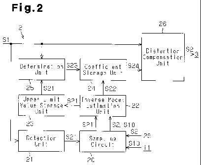
Fig. 2 is a block diagram showing a first example of the
DPD processor 2. As shown by the connection relation in Fig.
2, the DPD processor 2 includes a sampling circuit 20, a
detection unit 21, an inverse model estimation unit 22, an
upper limit value storage unit 23, a coefficient storage
unit 24, a determination unit 25, and a distortion
compensation unit 26.
The sampling circuit 20 receives the signal S2 from the
distortion compensation unit 26 and the signal S10 from the
ADC 11. The sampling circuit 20 samples the signals S2 and
S10 in a predetermined time immediately before the sampling
(hereinafter referred to as "sampling time") and inputs the
signals S2 and S10 to the inverse model estimation unit 22.
13
CA 02748192 2011-06-22
P3P2009216CA
The inverse model estimation unit 22 estimates a model
expressing input-output characteristics of the HPA 6 based
on the signals S2 and S10 and computes coefficients of each
order (i.e., coefficient set of an inverse model) to express
an inverse model of the estimated model in the form of a
polynomial of an nth-order power (in which n is a natural
number). To compensate for non-linear distortion in a model,
the distortion characteristics of the model are inverted in
an inverse model.
Further, the detection unit 21 detects a maximum level
(maximum power value, for example) of the input signal Si in
the sampling time and sends data S21, which is related to
the maximum power value, to the sampling circuit 20. The
data S21 is input from the sampling circuit 20 to the
inverse model estimation unit 22 and associated with the
inverse model coefficient, which is obtained as described
above. The maximum power value provided by the data S21
indicates an upper limit value for range covered by the
associated inverse model.
Data S22 related to the coefficient set of the inverse
model is input from the inverse model estimation unit 22 to
the coefficient storage unit 24 and stored in the
coefficient storage unit 24. In other words, the inverse
model is stored in the coefficient storage unit 24. Further,
the data S21 related to the maximum power value associated
with the inverse model is input from the inverse model
estimation unit 22 to the upper limit value storage unit 23
and stored in the upper limit value storage unit 23.
The distortion compensation unit 26 receives the input
signal Sl and data S24 related to the coefficient set from
14
CA 02748192 2011-06-22
P3P2009216CA
the coefficient storage unit 24. The distortion compensation
unit 26 corrects the input signal Sl based on the
coefficient set (inverse model) provided by the data S24.
This outputs the signal S2, which is obtained by performing
proper distortion compensation on the input signal Sl, from
the distortion compensation unit 26.
The input-output characteristics of the HPA 6 vary as
the temperature or the like changes. Thus, in order to
realize highly accurate distortion compensation, the inverse
model estimation unit 22 must always update the model and
inverse model to the latest ones.
Fig. 3 is a graph showing one example of a plurality of
models KO to K2 updated in sequence. The horizontal axis
indicates a signal level (for example, power value) of the
input signal Si and the vertical axis indicates the signal
level (for example, power value) of the output signal
(signal S10). The model KO is estimated by the inverse model
estimation unit 22 under a situation in which the amount of
communication data is large, and an upper limit value PmO of
the covered range conforms to a maximum value (peak value)
that the signal level of the input signal Sl can take.
Accordingly, by using the model K0, the inverse model
estimation unit 22 can generates an inverse model that
covers the entire range of the input signal Sl. The data S21
indicating the upper limit value PmO is associated with the
inverse model of the model KO and stored in the upper limit
value storage unit 23.
A model K1 obtained by updating the model KO is
estimated by the inverse model estimation unit 22 under a
situation in which the amount of communication data is
CA 02748192 2011-06-22
P3P2009216CA
relatively small, and an upper limit value Pml of the
covered range of the model Kl is smaller than the maximum
value PmO of the model KO. Accordingly, when an inverse
model generated from the model K1 is used, the distortion
compensation unit 26 may not perform distortion compensation
on the input signal S1 that has a signal level in excess of
the upper limit value Pml. However, in a range that is less
than or equal to the upper limit value Pml, the input-output
characteristics that are newer than the model KO can be
expressed by the model K1. Thus, highly accurate distortion
compensation can be realized. The data S21 indicating the
upper limit value Pml is associated with the inverse model
of the model Kl and stored in the upper limit value storage
unit 23.
The model K2 obtained by updating the model Kl is
estimated by the inverse model estimation unit 22 under a
situation in which the amount of communication data is
further smaller, and an upper limit value Pmt of the covered
range of the model K2 is smaller than the maximum value Pml
of the model Kl. Accordingly, when an inverse model
generated from the model K2 is used, the distortion
compensation unit 26 may not perform distortion compensation
on the input signal S1 having a signal level in excess of
the upper limit value Pm2. However, in a range that is less
than or equal to the upper limit value Pm2, the model K2
expresses the input-output characteristics that are newer
than the models KO and Kl. Thus, highly accurate distortion
compensation is realized. The data S21 indicating the upper
limit value Pm2 is associated with the inverse model of the
model K2 and stored in the upper limit value storage unit
23.
16
CA 02748192 2011-06-22
P3P2009216CA
In the DPD processor 2 of the present embodiment, the
coefficient sets of each of the inverse models corresponding
to the models KO to K2 are stored in the coefficient storage
unit 24. The distortion compensation unit 26 performs
distortion compensation on the input signal Si by selecting
the optimal one of the three inverse models corresponding to
the respective models KO to K2. This will now be described
in detail.
Fig. 4 is a graph for the selection of the inverse model
by the distortion compensation unit 26. The input signal Si
is input to the distortion compensation unit 26 and the
determination unit 25. Further, the determination unit 25
receives the data S21 related to the upper limit value of
the covered range of each inverse model from the upper limit
value storage unit 23. When the signal level of the input
signal Si is less than or equal to the upper limit value
Pm2, the determination unit 25 selects the inverse model
corresponding to the model K2. That is, when the signal
level of the input signal Si is less than or equal to the
upper limit value Pm2, the three inverse models
corresponding to the respective models KO K2 are present as
the inverse model that covers the signal level. In this
case, the determination unit 25 selects the latest one (the
inverse model corresponding to the model K2) of the three
inverse models. Data S23 related to the selection of the
inverse model is input to the coefficient storage unit 24
from the determination unit 25. Then, the data S24 related
to the coefficient set of the selected inverse model is
input from the coefficient storage unit 24 to the distortion
compensation unit 26. The distortion compensation unit 26
corrects the input signal Si based on the inverse model
having the coefficient set obtained by the data S24.
17
CA 02748192 2011-06-22
P3P2009216CA
In the same manner, when the signal level of the input
signal Si is greater than the upper limit value Pm2 and less
than or equal to the upper limit value Pml, the
determination unit 25 selects the inverse model
corresponding to the model Kl. That is, when the signal
level of the input signal Sl is greater than the upper limit
value Pm2 and les than or equal to the upper limit value
Pml, the two inverse models corresponding to the respective
models KO and K1 are present as the inverse model that
covers that signal level. In this case, the determination
unit 25 selects the latest one (the inverse model
corresponding to the model K1) of the two inverse models so
that the distortion compensation unit 26 corrects the input
signal Sl based on the selected inverse model.
Further, when the signal level of the input signal Si is
greater than the upper limit value Pml, only the inverse
model corresponding to the model KO is present as the
inverse model that covers the signal level. In this case,
the determination unit 25 selects the inverse model
corresponding to the model KO, and the distortion
compensation unit 26 corrects the input signal Sl based on
the selected inverse model.
In the foregoing description illustrates an example in
which models are updated in a descending order in which the
upper limit value becomes smaller (models KO -* K1 K2).
In contrast, if the models are updated in the order of K1 -*
KO -> K2), when the inverse model corresponding to the model
KO is stored in the coefficient storage unit 24, the inverse
model corresponding to the model Kl may be deleted from the
coefficient storage unit 24. In this case, the determination
18
CA 02748192 2011-06-22
P3P2009216CA
unit 25 selects the inverse model corresponding to the model
K2 when the signal level of the input signal Sl is less than
or equal to the upper limit value Pm2, and the determination
unit 25 selects the inverse model corresponding to the model
KO when the signal level of the input signal Sl is greater
than the upper limit value Pm2.
Fig. 5 is a block diagram showing a second example of
the DPD processor 2. This configuration is the same as that
shown in Fig. 2 except in that a comparison unit 30 is
added.
Fig. 6 is a graph showing one example of the plurality
of models K0-K3 corresponding to Fig. 3. A predetermined
threshold value H is set for the signal level of the input
signal S1. The threshold value H is set, for example, to a
value that is one half of the maximum value (peak value)
that the input signal Sl can take. However, the threshold
value H may be set to any other value. The set value of the
threshold value H is taught beforehand to the comparison
unit 30.
When the inverse model estimation unit 22 estimates an
inverse model, the comparison unit 30 compares the maximum
value of the input signal Si (i.e., an upper limit value
obtained from the data S21) in a range in which the sampling
circuit 20 performs sampling with the threshold value H.
Then, results of the comparison are input as data S30 to the
inverse model estimation unit 22. The inverse model
estimation unit 22 updates the inverse model when determined
that the maximum value of the input signal Sl in the
sampling range is greater than or equal to the threshold
value H based on the data S30. In contrast, when the maximum
19
CA 02748192 2011-06-22
P3P2009216CA
value of the input signal Si in the sampling range is less
than the threshold value H, the inverse model is not
updated. In the example shown in Fig. 6, the inverse models
corresponding to the models K0, K1, and K2 are updated.
However, the inverse model corresponding to the model K2 is
not updated to the inverse model corresponding to the model
K3 because the upper limit value (i.e., the maximum value of
the input signal Sl in the sampling range when estimating
the model K3) of the covered range of the model K3 is less
than the threshold value H.
Fig. 7 is a graph showing another example of the
plurality of models K0-K2 corresponding to Fig. 3. A
plurality of predetermined threshold values HO and Hl are
set for the signal level of the input signal Si. The
threshold value HI is set to, for example, one half of the
maximum value (peak value) that the input signal S1 can
take. The threshold value HO is set to, for example, an
intermediate value between the peak value and the threshold
value H1. However, the threshold values HO and H1 may be set
to other values. Further, the number of the threshold values
is not limited to two but may be three or more (for example,
four). The set values of the threshold values HO and H1 are
taught beforehand to the comparison unit 30.
When the inverse model estimation unit 22 estimates an
inverse model, the comparison unit 30 compares the maximum
value of the input signal S1 in the sampling range with the
threshold values HO and Hl. Then, the results of the
comparison are input as the data S30 to the inverse model
estimation unit 22.
When updating the inverse model corresponding to the
CA 02748192 2011-06-22
P3P2009216CA
model KO including the peak value to an inverse model having
an upper limit value of a smaller covered range, the inverse
model estimation unit 22 performs updating under the
condition that the upper limit value of the updated inverse
model is a value in the presently set update range, in this
case, the threshold value HO. That is, when the upper limit
value of the updated inverse model is the threshold value HO
or larger, updating is performed based on the data S30. When
the upper limit value is less than the threshold value HO,
updating is not performed. In the example shown in Fig. 7,
the upper limit value Pml of the model K1 is greater than or
equal to the threshold value HO. Thus, the inverse model
corresponding to the model KO is updated to the inverse
model corresponding to the model Kl. However, the upper
limit value Pm2 of the model K2 is less than the threshold
value HO. Thus, the inverse model corresponding to the model
KO is not directly updated to the inverse model
corresponding to the model K2. In the example shown in Fig.
7, instead of the data S21 indicating the upper limit value
PmO, flag information indicating that the signals S2 and Sl0
cover the peak value is input from the sampling circuit 20
to the inverse model estimation unit 22 in association with
the signals S2 and S10. In the same manner, in the example
shown in Fig. 7, instead of the data S21 indicating the
upper limit value Pml, flag information indicating that the
signals S2 and S10 cover the threshold value HO is input
from the sampling circuit 20 to the inverse model estimation
unit 22 in association with the signals S2 and S10.
When the inverse model estimation unit 22 updates the
inverse model corresponding to the model K1, of which upper
limit value is greater than or equal to the threshold value
HO, to an inverse model having a covered range with a
21
CA 02748192 2011-06-22
P3P2009216CA
smaller upper limit value, the inverse model estimation unit
22 performs updating under the condition that the upper
limit value of the updated inverse model is greater than or
equal to a value in the presently set update range, in this
case, the threshold value Hl. That is, when the upper limit
value of the updated inverse model is greater than or equal
to the threshold value Hl, the inverse model estimation unit
22 performs updating based on the data S30. When the upper
limit value is less than the threshold value Hl, the inverse
model estimation unit 22 does not perform updating. In the
example shown in Fig. 7, the upper limit value Pm2 of the
model K2 is greater than or equal to the threshold value Hl.
Thus, the inverse model corresponding to the model Kl is
updated to the inverse model corresponding to the model K2.
In the same manner as described above, in the example shown
in Fig. 7, instead of the data S21 indicating the upper
limit value Pm2, flag information indicating that the
signals S2 and S10 cover the threshold value Hl is
associated with the signals S2 and Sl0 and input from the
sampling circuit 20 to the inverse model estimation unit 22.
Fig. 8 is a graph corresponding to Fig. 7 and used by
the coefficient storage unit 24 to select an inverse model.
The threshold values HO and H1, which are set in the
comparison unit 30, are stored also in the upper limit value
storage unit 23. When the signal level of the input signal
Sl is less than or equal to the threshold value Hl, the
determination unit 25 generates the data S23 related to the
selection of an inverse model that corresponds to the
portion of the latest model K2 in this range that is less
than or equal to the threshold value Hl. The distortion
compensation unit 26 corrects the input signal Sl based on
the coefficient set of an inverse model selected in the
22
CA 02748192 2011-06-22
P3P2009216CA
coefficient storage unit 24 in accordance with the data S23.
Further, when the signal level of the input signal S1 is
greater than the threshold value Hl and less than or equal
to the threshold value HO, the distortion compensation unit
26 corrects the input signal Sl based on an inverse model
that corresponds to the portion of the latest model K1 in
this range that is greater than the threshold value H1 and
less than or equal to the threshold value HO. Further, when
the signal level of the input signal Sl is greater than the
threshold value HO, the distortion compensation unit 26
corrects the input signal Sl based on an inverse model that
corresponds to the portion of the latest model KO in this
range that is greater than the threshold value HO. In this
manner, the entire signal level region over which the input
signal Sl can take is divided into a plurality of regions by
at least two threshold values. For example, when the present
inverse model is KO as shown in Fig. 8, a power value range
of 0 (zero) to PmO for the input signal Sl is divided into
three regions (0 to Hl, H1 to HO, and HO to PmO) by the two
threshold values HO and Hl. Then, the determination unit 25
selects one of the inverse models (the latest one when there
are two or more inverse models) in each of the partial
regions.
Fig. 9 is a block diagram showing a third example of the
DPD processor 2. This configuration is the same as that
shown in Fig. 2 except in that a setting unit 40 is added.
The setting unit 40 obtains an average value of the
signal level (for example, power value) of the input signal
Sl in a given period immediately before start of sampling
circuit 20 starts sampling. Further, the setting unit 40
sets a value that is higher than the average value by a
23
CA 02748192 2011-06-22
P3P2009216CA
predetermined level (10-11 dBm, for example) as a predicted
maximum value of the input signal S1. The upper limit of the
predicted maximum value is assumed to be a maximum value
(peak value) that the input signal Sl can take. Data S40
related to the predicted maximum value is input from the
setting unit 40 to the detection unit 21.
When the sampling circuit 20 starts sampling, the
detection unit 21 consecutively monitors the signal level of
the sampled input signal Sl. Then, when detecting the input
signal Sl having at least the predicted maximum value
obtained from the data S40, the detection unit 21 provides
the sampling circuit 20 with data S41 indicating such state.
When received the data S41, the sampling circuit 20
immediately ends sampling. When the input signal Sl having
at least the predicted maximum value obtained from the data
S40 is not detected by the detection unit 21, the sampling
circuit 20 ends sampling after the predetermined time
elapses from when the sampling starts.
In this manner, in the DPD processor 2 (distortion
compensation circuit) of the present embodiment, the inverse
model estimation unit 22 updates an inverse model based on
the signals S2 and S10 received from the sampling circuit 20
regardless of whether or not the maximum value (peak value)
that the input signal Sl can take is included in the range
sampled by the sampling circuit 20. Thus, the inverse model
estimation unit 22 can update the model even under a
situation in which the appearance frequency of the input
signal Sl having the maximum value (peak value) is low.
Further, the inverse model is updated accordingly. This
allows for highly accurate distortion compensation to be
realized in the distortion compensation unit 26.
24
CA 02748192 2011-06-22
P3P2009216CA
In the DPD processor 2 shown in Figs. 5 and 6, the
inverse model estimation unit 22 updates an inverse model
under the condition that the maximum value of the input
signal Sl in the range sampled by the sampling circuit 20 is
greater than or equal to the predetermined value H.
Accordingly, when the signal level of the input signal Si in
the sampled range is less than the threshold value H, the
inverse model is not updated. This prevents the range of the
input signal Si covered by the inverse model from becoming
too small. The threshold value may be fixed or variable.
In the DPD processor 2 shown in Fig. 7, the plurality of
threshold values HO and Hl are set in accordance with an
upper limit value of the input signal Sl in the present
inverse model. In other words, the threshold values HO and
Hl are always varied in accordance with the maximum value
(peak value) of the input signal Si. For example, in Fig. 7,
when the present inverse model is model K1, the threshold
value Hl is set to one half of the maximum value Pmt, and
the threshold value HO is set to an intermediate value
between the maximum value Pml and the threshold value Hl
(one half of the maximum value Pml). In this state, when the
inverse model is updated from model K1 to model KO, the
threshold value Hl is changed to one half of. the maximum
value PmO, and the threshold value HO is changed to the
intermediate value between the maximum value PmO and the
threshold value Hl (one half of the maximum value PmO).
Accordingly, the use of the threshold values HO and Hl
prevents the range of the input signal Si covered by the
inverse model from suddenly becoming small. For example, the
inverse model corresponding to the model KO can be avoided
from being directly updated to the inverse model
CA 02748192 2011-06-22
P3P2009216CA
corresponding to the model K2.
In the DPD processor 2 shown in Fig. 9, the setting unit
40 sets a predicted maximum value for the input signal Si.
After the sampling circuit 20 starts sampling, when the
input signal Sl of the predicted maximum value or greater is
detected, the sampling circuit 20 ends sampling. This
shortens the sampling period and ensures that the input
signal Sl having the predicted maximum value is obtained.
Thus, the generation of an inverse model that covers a range
of the predicted maximum value or less is ensured.
Further, in the wireless base station 1 of the present
embodiment, distortion of the input-output characteristics
of the HPA 6 is properly compensated by the DPD processor 2.
This allows for the desired transmission signal to be
transmitted from the wireless base station 1.
The disclosed embodiments are exemplary in all respects
and not restrictive. The present is not to be limited to the
details given herein, but may be modified within the scope
and equivalence of the appended claims.
26