Note: Descriptions are shown in the official language in which they were submitted.
CA 02749329 2011-07-11
WO 2010/083091 PCT/US2010/020364
PULSE TEMPORAL PROGRAMMABLE ULTRAFAST BURST MODE LASER FOR
MICROMACHINING
Technical Field
[0001] The present disclosure relates to laser micromachining. In particular,
the
present disclosure relates to laser systems and methods that use a burst of
ultrafast
laser pulses.
Background Information
[0002] After manufacture of a semiconductor memory array chip is complete,
integrated circuit (IC) patterns on an exposed surface of the chip are sealed
with an
electrically insulating layer of passivating material. Typical passivating
materials
include resins or thermoplastic polymers such as, for example, polyimide. The
purpose of this final "passivation" layer is to prevent the surface of the
chip from
reacting chemically with ambient moisture, to protect the surface from
environmental
particulates, and to absorb mechanical stress. Following passivation, the chip
is
mounted in an electronic package embedded with metal interconnects that allow
probing and functional testing of the memory cells. When one of many redundant
memory cells is determined to be faulty, the cell is disabled by severing the
conductive interconnects, or wires, linking that cell to its neighbors in the
array.
Disabling individual memory cells by "link processing" or "link blowing" is
accomplished by laser micromachining equipment that is capable of directing
laser
beam energy so as to selectively remove the link material in a highly
localized region
without imparting damage to the materials adjacent to, below, or above the
target.
Selectively processing a designated link may be achieved by varying the laser
beam
wavelength, spot size, pulse repetition rate, pulse shape, or other spatial or
temporal
beam parameters that influence energy delivery.
[0003] Laser micromachining processes that entail post-processing of
electrically
conductive links in memory arrays or other types of IC chips use sharp pulses
with a
fast rising front edge (e.g., with a 1-2 nanosecond rise time) to achieve
desired
quality, yield, and reliability. To cleanly sever a link, the laser pulse
penetrates the
overlying passivation layer before cutting through the metal interconnect. The
rising
edge of a typical pulse from an existing solid-state laser varies with pulse
width. Use
of a traditional Gaussian-shaped laser pulse having a 5-20 nanosecond pulse
width
and a sloped, gradually rising front edge in link processing tends to cause an
"over
1
CA 02749329 2011-07-11
WO 2010/083091 PCT/US2010/020364
crater" in the passivation layer, especially if its thickness is too large or
is uneven.
Over cratering reduces the reliability of IC chips.
[0004] Rupture behavior of overlying passivation layers has been well analyzed
by Yunlong Sun in his PhD dissertation entitled, "Laser processing
optimization of
semiconductor based devices" (Oregon Graduate Institute, 1997). Because
passivation layer thickness is an important parameter, the optimal thickness
of a
particular passivation layer material may be determined by simulations based
on
Sun's analysis. Difficulty in maintaining wafer-level process control of the
passivation layer during IC fabrication may result in non-optimal thickness
and poor
cross-wafer or wafer-to-wafer thickness uniformity. Therefore, optimizing
characteristics of laser pulses used in post-processing may help to compensate
for
mis-targeted dimensions and sources of variation in the passivation layer.
[0005] U.S. Patent No. 6,281,471 of Smart proposes using substantially square-
shaped laser pulses for link processing. Such a sharp-edged pulse may be
generated by coupling a master oscillator laser with a fiber amplifier (MOPA).
This
low power master oscillator employs a diode laser that is capable of
generating a
square-shaped pulse with a fast rise time. On the other hand, U.S. Patent No.
7,348,516 of Yunlong Sun et al., which patent is assigned to the assignee of
this
patent application, states that, despite a vertical rising edge, a
substantially square-
shaped laser pulse is not the best laser pulse shape for link processing.
Instead,
Sun, et al. describes use of a specially tailored laser pulse shape that, in
one
embodiment, resembles a chair, with a fast rising peak or multiple peaks to
most
effectively process links, followed by a drop-off in signal strength that
remains
relatively flat at a lower power level before shutting off. Such a tailored
laser pulse,
with high peak power but low average power, has been successfully generated by
what is called pulse slicing technology, which can be implemented by either
electro-
optical modulation (EOM) or acousto-optical modulation (AOM). For example, a
conventional active Q-switched solid-state laser provides nanosecond seed
pulses
with high intensity and high pulse energy, and then a light-loop slicing
device
transforms a standard laser pulse into a desired tailored pulse shape.
[0006] U.S. Patent Application No. 12/057,264, of Xiaoyuan Peng et al., which
application is assigned to the assignee of the present patent application,
teaches a
light-loop slicing scheme implemented, for example, in an ultraviolet (UV)
laser
system for semiconductor link processing. Alternatively, a specially tailored
laser
2
CA 02749329 2011-07-11
WO 2010/083091 PCT/US2010/020364
pulse may be generated by a MOPA that employs a gain fiber as the power
amplifier. Using a MOPA is advantageous in that it constitutes a stable signal
source
at a specified constant frequency.
[0007] U.S. Patent Application No. 2006/0159138 of Pascal Deladurantaye
describes a shaped-pulse laser in which two modulators shape a continuous wave
(CW) light beam to generate various shaped pulses. However, generating a
pulsed
laser from a CW light beam is fairly inefficient, and thus requires more
amplification.
Because such a low peak-power signal may be influenced by noise, which causes
pulse-to-pulse instability, the two modulators are preferably synchronized to
maintain
pulse stability and energy stability, thereby adding further complexity and
cost.
[0008] The above systems and methods generally use laser pulses with pulse
widths in the nanosecond range. However, the 1 pm and 1.3 pm laser wavelengths
with pulse widths in the nanosecond range have disadvantages. For example, the
energy coupling efficiency of such infrared (IR) laser beams into a highly
electrically
conductive metallic link is relatively poor. Further, the practical achievable
spot size
of an IR laser beam for link severing is relatively large and limits the
critical
dimensions of link width, and link pitch. As has been discussed in detail by
Yunlong
Sun, "Laser Processing Optimization for Semiconductor Based Devices"
(unpublished doctoral thesis, Oregon Graduate Institute of Science and
Technology,
1997), conventional laser link processing with nanosecond pulse width may rely
on
heating, melting, and evaporating the link, and creating a mechanical stress
build-up
to explosively open the overlying passivation layer with a single laser pulse.
Such a
conventional link processing laser pulse creates a large heat affected zone
(HAZ)
that could deteriorate the quality of the device that includes the severed
link. For
example, when the link is relatively thick or the link material is too
reflective to absorb
an adequate amount of the laser pulse energy, more energy per laser pulse is
used
to sever the link. Increased laser pulse energy increases the damage risk to
the IC
chip, including irregular or over sized opening in the overlying passivation
layer,
cracking in the underlying passivation layer, damage to the neighboring link
structure
and damage to the silicon (Si) substrate. However, using laser pulse energy
within
a risk-free range on thick links often results in incomplete link severing.
[0009] Thus, investigations have been performed for using ultrafast lasers
(either
picosecond or femtosecond lasers) to process semiconductor materials such as
links
in IC chips. However, the high peak power of a single ultrafast pulse may
easily
3
CA 02749329 2011-07-11
WO 2010/083091 PCT/US2010/020364
damage the underlying Si substrate, which is unacceptable in many
applications.
One solution to the problem of high peak power substrate damage caused by
ultrafast lasers is to use a burst or train of ultrafast pulses with smaller
peak powers.
A pulse train also has the effect of producing a smaller effective spot size
in the
material. A problem with using a train of ultrafast pulses is that many
commercially
available ultrafast lasers that use a pulse picker have pulse repetition rates
in the
kilohertz range. Without the pulse picker, a mode-locked laser runs at a fixed
repetition rate that is typically in the tens of megahertz range. Such a
repetition rate
may be difficult to apply to links because stage movement is typically
approximately
400 mm/s such that the laser spot may move off a targeted link in less than
approximately 500 nanoseconds. Thus, lasers used for pulse train applications
may
require pulse repetition rates starting at approximately 100 MHz.
[0010] U.S. Patent Application No. 2007/0199927, of Bo Gu at al., uses a laser
with at least one pulse having a pulse duration in a range between
approximatley 10
picoseconds and less than appoximately 1 nanosecond. Achim Nebel et at. from
Lumera Laser GmbH have demonstrated a passively mode-locked laser that uses
digital timing control to generate sequences or groups of pulses. See,
"Generation
of Tailored Picosecond-Pulse-Trains for Micro-Machining," Photonics West 2006,
LASE Conference: Commercial and Biomedical Applications of Ultrafast Lasers VI
Paper No. 6108-37. The system taught by Achim Nebel et al. is based on a
"double-
switch" scheme generated by high-voltage electro-optical (EO) pulse-picker
that
drives a voltage passing a half wave of a Pockels cell and generates two HV
pulses
in one cycle. The delay time between groups of pulses is changeable. This
feature
provides certain flexibility for material processing. However, the envelope of
a burst
of pulses is not capable of being changed, which limits use of the system in
various
micromachining applications. In addition, the solution provided by Achim Nebel
et al.
is large and costly. The mechnical and thermal requirements are fairly high
due to a
long cavity length, which is generally more than 1 meter for an 80 MHz mode-
locked
cavity.
Summary of the Disclosure
[0011] In one embodiment, a laser system is configured for processing a
material
with a selectively shaped burst of ultrafast laser pulses. The system includes
a burst
pulse laser configured to emit a burst of three or more laser pulses defined
by a
selectively shaped burst envelope. The burst pulse laser is further configured
to
4
CA 02749329 2011-07-11
WO 2010/083091 PCT/US2010/020364
selectively adjust temporal spacing between the three or more laser pulses
within the
burst envelope and the temporal width of the burst envelope. The system also
includes one or more amplifiers configured to amplify the group of three or
more
laser pulses so as to obtain a desired shape of the burst envelope. In certain
embodiments, the burst pulse laser includes a laser source configured to emit
a train
of laser pulses, and an optical modulator that receives the train of laser
pulses. The
optical modulator is configured to amplitude modulate the train of laser
pulses so as
to generate the burst of three or more laser pulses defined by the selectively
shaped
burst envelope.
[0012] In another embodiment, a method for processing a material with a
selectively shaped burst of ultrafast laser pulses includes providing a train
of laser
pulses at a first repetition rate, modulating the train of laser pulses based
on a
selectively shaped burst envelope, and selectively adjusting the spacing
between the
three or more laser pulses within the burst envelope. The modulation includes
amplitude adjusting three or more laser pulses within the burst envelope.
[0013] Additional aspects and advantages will be apparent from the following
detailed description of preferred embodiments, which proceeds with reference
to the
accompanying drawings.
Brief Description of the Drawings
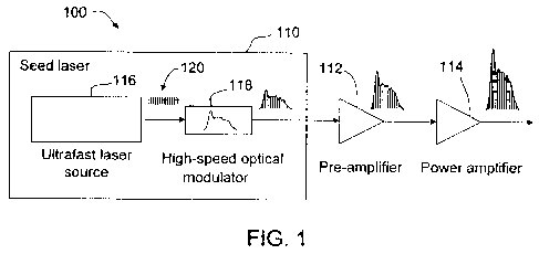
[0014] FIG. 1 is a block diagram of a laser system having a programmable burst
pulse laser according to one embodiment.
[0015] FIG. 2 is a block diagram of an ultrafast laser source according to one
embodiment that includes a high-speed distributed feedback diode.
[0016] FIG. 3 is a block diagram of a typical fiber mode-locked master
oscillator
that may be used as the ultrafast laser source of FIG. 1 according to one
embodiment.
[0017] FIG. 4 graphically illustrates example burst envelopes that may be
produced according to certain embodiments.
[0018] FIG. 5 is a block diagram of a seed laser usable by the laser system to
generate shaped burst envelopes according to one embodiment.
[0019] FIG. 6 is a block diagram of a laser system with a seed laser that
selectively combines the outputs of a first ultrafast laser source and a
second
ultrafast laser source according to one embodiment.
CA 02749329 2011-07-11
WO 2010/083091 PCT/US2010/020364
[0020] FIGS. 7A, 7B, and 7C are block diagrams of respective laser systems
implementing different pre-amplifier (phase 1) and power amplifier (phase 2)
configurations according to certain embodiments.
[0021] FIG. 8 is a block diagram of a laser system that includes a harmonic
generator for wavelength conversion according to one embodiment.
[0022] FIGS. 9A, 9B, 9C, and 9D illustrate various examples of the interaction
of
a laser beam with a workpiece according to certain embodiments.
Detailed Description of Preferred Embodiments
[0023] A laser processing system according to one embodiment generates
ultrafast laser pulses with a temporal programmable burst mode. A burst pulse
laser
includes a high repetition rate ultrafast laser configured to deliver a pulse
train with
each pulse in the train having an independently controlled amplitude. The
respective
amplitudes of each ultrafast pulse in a group or "burst" of pulses, along with
the
spacing between pulses, define a "burst envelope." In addition to
independently
controlling the amplitude of each ultrafast pulse in a burst of pulses, the
system may
also provide selective control of spacing between each ultrafast pulse and/or
the
overall temporal width of the burst envelope. Thus, the system provides
selective
shaping of the burst envelope for particular laser processing applications.
Because
each ultrafast pulse within the group of pulses may have a temporal width in a
picosecond range, or even a femtosecond range, the laser system may be used,
for
example, for efficient and high quality material processing.
[0024] In certain embodiments, as discussed in detail below, the laser system
includes a seed laser having an ultrafast laser source and a high-speed
optical
modulator to shape the burst envelope. The laser system also includes one or
more
amplifier stages to amplify the shaped burst of laser pulses before the system
applies it to a work surface. The ultrafast laser source may include a
semiconductor
laser, a fiber laser, or a solid-state laser. In certain embodiments, the
ultrafast laser
source may be a linearly polarized, narrow bandwidth source. Thus, the system
may
use harmonic generation to provide shorter wavelengths and/or Raman and
optical
parametric generation (OPO) to provide longer wavelengths. The programable
shape may be obtained by using, for example, pulse picking, high-speed
modulation,
seed source eletrical modulation in the case of semiconductor gain-switched
ultrafast
laser, or a combination of the foregoing. A pre-amplifier may include, for
example,
photonic crystals, a large mode area (LMA) gain fiber, or a single mode gain
fiber. A
6
CA 02749329 2011-07-11
WO 2010/083091 PCT/US2010/020364
post amplifier (power amplifier) may include, for example, a solid-state gain
medium.
As discussed below, in certain embodiments, the pre-amplifier and post
amplifier
may inlcude any combination of fiber or solid-state amplifiers. The
embodiments
disclosed herein provide a versatile ultrafast laser source for high quality
material
processing in many different applications.
[0025] Reference is now made to the figures in which like reference numerals
refer to like elements. For clarity, the first digit of a reference numeral
indicates the
figure number in which the corresponding element is first used. In the
following
description, numerous specific details are provided for a thorough
understanding of
the embodiments disclosed herein. However, those skilled in the art will
recognize
that the embodiments described herein can be practiced without one or more of
the
specific details, or with other methods, components, or materials. Further, in
some
cases, well-known structures, materials, or operations are not shown or
described in
detail in order to avoid obscuring aspects of the embodiments. Furthermore,
the
described features, structures, or characteristics may be combined in any
suitable
manner in one or more embodiments.
[0026] FIG. 1 is a block diagram of a laser system 100 according to one
embodiment. The laser system 100 includes a seed laser 110, a pre-amplifier
112,
and a power amplifier 114. The seed laser 110 includes an ultrafast laser
source
116 and a high-speed optical modulator 118. The ultrafast laser source 116
provides a train of ultrafast laser pulses 120 to the high-speed optical
modulator 118.
In one embodiment, the temporal pulse width of each ultrafast laser pulse 120
is in a
range between approximately 300 femtoseconds and approximately 1 nanosecond.
[0027] The ultrafast laser source 116 provides the ultrafast laser pulses 120
at a
high repetition rate. In one embodiment, the ultrafast laser source 116
operates at a
repetition rate in a range between approximately 1 Hz and approximately 100
kHz.
In other embodiments, the repetition rate is in a range between approximately
100
kHz and approximately 80 MHz. An artisan will recognize from the disclosure
herein
that much higher repetition rates may also be used. For example, in some
embodiments repetition rates as high as 500 MHz or higher may be used. In
another
embodiment, repetition rates may be as high as approximately 10 GHz or higher.
[0028] In one embodiment, the ultrafast laser source 116 includes a high-speed
ultrafast semiconductor diode. For example, FIG. 2 is a block diagram of an
ultrafast
laser source 116 according to one embodiment that includes a high-speed
7
CA 02749329 2011-07-11
WO 2010/083091 PCT/US2010/020364
distributed feedback (DFB) diode 210. The DFB diode 210 is modulated by a seed
pulse signal 212 produced by a high-speed driver 214 to provide at a high
repetition
rate the train of ultrafast laser pulses 120. In certain embodiments, the
laser source
116 includes an optical modulator. For example, the laser source 116 may
include a
20 GHz bandwidth modulator capable of providing 50 picosecond pulse widths. An
artisan will recognize from the disclosure herein that the optical modulator
may
operate above or below 20 GHz. For example, in one embodiment the optical
modulator may operate at a bandwidth of up to approximately 40 GHz.
[0029] Using the DFB diode 210 as the laser source 116 offers wide tunability,
narrow linewidth, and high output power in a compact and very rugged setup.
For
example, a frequency selective element (not shown) within the DFB diode 210,
such
as a Bragg grating, is integrated into the active section of the
semiconductor. Thus,
single-frequency operation and high coherence (e.g., a coherence length in a
range
between approximately 50 m and approximately 200 m) are obtained without any
bulk optics, making the DFB diode 210 particularly suitable for use within
harsh
industrial environments or for airborne applications.
[0030] The DFB diode 210 shown in FIG. 2 may be tuned according to certain
embodiments by changing either the temperature (e.g., typically at a tuning
rate of
approximately 25 GHz/K) or the operating current (e.g., typically at a tuning
rate of
approximately 1 GHz/mA to approximately 2 GHz/mA). While current-tuning is
favorable for rapid modulation tasks, thermal tuning has the advantage of
providing
extremely large mode-hop free tuning ranges (e.g., up to approximately 1200
GHz).
Generally, the wavelength of a DFB laser is tuned by varying the laser current
or the
chip temperature. Electric modulation is suitable for fast frequency scans
within a
small range (e.g., for linewidths in a range between approximately 0.1 nm and
approximately 0.2 nm at modulation frequencies in the kHz to MHz range).
Larger
tuning ranges of up to approximately 3 nm are realized by varying the laser
temperature, typically over an interval of approximately 40 C.
[0031] By way of example, the DFB diode 210 may be a DFB diode equipped
with polarization maintaining (PM) fiber couplers (not shown) may be obtained
from
Toptica Photonics, AG of Munich, Germany. As another example, the diode 210
may include an ultrafast gain-switched diode with a direct modulated source
providing 50 picosecond pulse widths, as demonstrated by PicoQuant GmbH, of
Berlin, Germany.
8
CA 02749329 2011-07-11
WO 2010/083091 PCT/US2010/020364
[0032] Returning to FIG. 1, in other embodiments, the ultrafast laser source
116
may include a solid-state ultrafast laser, a passively mode-locked fiber
master
oscillator, a combination of multi-fiber master oscillators, a passively mode-
locked
semiconductor laser, or any other high repetition rate ultrafast laser. For
example,
FIG. 3 is a block diagram of a typical fiber mode-locked master oscillator
that may be
used as the ultrafast laser source 116 of FIG. 1 according to one embodiment.
In
the example shown in FIG. 3, the fiber mode-locked master oscillator includes
a
single mode gain fiber (SMF) 310 that forms a laser resonator terminated on
one end
by a semiconductor saturable absorber mirror (SESAM) 312 and on the other end
by
wavelength selector such as a fiber grating 314. The gain fiber 310 is pumped
by,
for example, a laser diode (not shown), the output of which is introduced to
the
resonator through a wavelength division multiplexer (WDM) 316. In operation,
the
fiber mode-locked master oscillator shown in FIG. 3 generates the train of
ultrafast
laser pulses 120 at a high repetition rate, as discussed above. The pulse
repetition
rate of the fiber mode-locked master oscillator is determined by the
resonator's
length.
[0033] As shown in FIG. 1, the train of ultrafast laser pulses 120 is provided
to the
high-speed optical modulator 118, which independently adjusts the amplitude of
each pulse so as to obtain a desired burst envelope shape for a particular
material
processing application. The high-speed optical modulator 118 may be programmed
to control the temporal spacing of the ultrafast pulses under the envelope,
the burst
envelope's temporal width, and/or the burst envelope's amplitude and
particular
shape. The programable burst envelope may be obtained by using, for example,
pulse picking (e.g., selecting pulses so as to control the distance between
pulses or
the pulse repetition frequency), high-speed modulation, seed source eletrical
modulation in the case of semiconductor gain-switched ultrafast laser, or a
combination of the foregoing. In one embodiment, the high-speed optical
modulator
118 includes a Mach-Zehnder interferometer (not shown) that modulates the
power
of the train of ultrafast laser pulses to obtain a desired burst envelope.
[0034] The temporal width of the burst envelope according to one embodiment is
in a range between approximately 10 picoseconds and approximately 1
nanosecond.
In other embodiments, the temporal width of the burst envelope is in a range
between approximately 1 nanosecond and approximately 10 nanoseconds. In other
embodiments, the temporal width of the burst envelope is in a range between
9
CA 02749329 2011-07-11
WO 2010/083091 PCT/US2010/020364
approximately 10 nanoseconds and approximately 100 nanoseconds. In other
embodiments, the temporal width of the burst envelope is in a range between
approximately 100 nanoseconds and approximately 1 microsecond. The burst
envelope may have other temporal widths depending on the particular
application.
[0035] In one embodiment, the rise time and/or fall time of the burst envelope
is
less than 1 nanosecond. For example, the rise time and/or fall time may be in
a
range between approximately 10 picoseconds and approximately 1 nanosecond.
Faster or slower rise/fall times may also be used for different applications.
For
example, the rise time and/or fall time may be in a range between
approximately 1
nanosecond and approximately 5 nanoseconds. The laser system's ability to a
provide burst envelope with a fast rise time and/or fall time is useful, for
example, to
link severing applications because it reduces the risk of generating over
craters in
the overlying passivation layer.
[0036] The pre-amplifier 112 and the power amplifier 114 provide appropriate
amplification to the shaped burst of ultrafast laser pulses provided at the
ouput of the
high-speed optical modulator 118. The pre-amplifier 112 according to certain
embodiments may include photonic crystals, LMA gain fiber, or single mode gain
fiber. In addition, or in other embodiments, the power amplifier 114 includes
a solid-
state gain medium. As discussed below, in certain embodiments, the pre-
amplifier
112 and the power amplifier 114 may include any combination of fibe or solid
state
amplifiers.
[0037] FIG. 4 graphically illustrates example burst envelopes that may be
produced according to certain embodiments. While FIG. 4 illustrates ten
different
burst envelope shapes (a), (b), (c), (d), (e), (f), (g), (h), (i), and (j), an
artisan will
recognize that the illustrated shapes are provided by way of example only and
that
any number of different burst envelope shapes may be produced according to the
systems and methods disclosed herein. Further, as discussed above, the
selected
envelope shape may be based on a particular material processing application.
[0038] For example, U.S. Patent No. 7,348,516 of Yunlong Sun et al., which
patent is assigned to the assignee of this patent application, describes the
use of a
specially tailored laser pulse shape that, in one embodiment, resembles a
chair, with
a fast rising peak or multiple peaks to most effectively process links,
followed by a
drop-off in signal strength that remains relatively flat at a lower power
level before
shutting off. Such a chair-shaped pulse corresponds to the burst envelope
shape (h)
CA 02749329 2011-07-11
WO 2010/083091 PCT/US2010/020364
shown in FIG. 4. In other material processing applications, multiple peaks may
be
used, such as shown in the burst envelope shapes (c), (d), and (e) in FIG. 4,
to
sequentially heat the material, remove a portion of the material to create a
kerf, and
clean out the kerf. Because the ultrafast laser source 116 combined with the
high-
speed optical modulator 118 is capable of providing various pulse shapes
containing
ultrafast pulses in the envelope with fine structures, many other burst
envelope
shapes for many different applications will occur to those skilled in the art
based on
the embodiments herein.
[0039] FIG. 5 is a block diagram of a seed laser 110 usable by the laser
system
100 to generate shaped burst envelopes according to one embodiment. The seed
laser 110 shown in FIG. 5 includes an ultrafast laser source 116, a pulse
picker 510,
and a pulse shaper 512. The ultrafast laser source 116 in this embodiment is a
fiber
mode-locked master oscillator that includes, as discussed above in relation to
FIG. 3,
the SMF 310, the SESAM 312, the fiber grating 314, and the WDM 316.
[0040] The pulse picker 510 may include, for example, an acousto-optical (AO)
modulator or an electro-optical (EO) modulator that is configured to change
the
repetition rate of the train of ultrafast pulses 120. As mentioned above, the
main
mode-lock frequency is determined by the resonator's length, which is fixed
for a
given oscillator. For example, the mode lock frequency may be approximately 1
GHz, which may not be ideal for processing certain materials. Thus, the pulse
picker
510 passes the pulses provided by the fiber mode-locked master oscillator at a
selected rate to lower the repetition rate (e.g., to change it from
approximately 1 GHz
to approximately 500 MHz or to a much lower rate such as to a few Hertz), as
represented in FIG. 5 by the train of ultrafast laser pulses 514. As another
example,
additional temporal delay may be added between two ultrafast laser pulses in a
burst
to allow heat dissipation. Thus, the pulse picker 510 may be used to
selectively
change the spacing between ultrafast laser pulses to control heating during
material
processing.
[0041] The pulse shaper 512 may include, for example, an EO modulator that is
configured to selectively provide amplitude modulation to each pulse in the
train of
ultrafast laser pulses 514. Thus, the pulse shaper 512 selectively shapes the
burst
envelope 516, as shown in FIG. 5. As discussed in relation to FIG. 1, the
shaped
burst of laser pulses may then be provided to the pre-amplifier 112 and the
power
amplifier 114 before being applied to a workpiece.
11
CA 02749329 2011-07-11
WO 2010/083091 PCT/US2010/020364
[0042] Repetition rates may be increased and further controlled by selectively
combining two or more ultrafast laser sources. For example, FIG. 6 is a block
diagram of a laser system 100 with a seed laser 110 that selectively combines
the
outputs of a first ultrafast laser source 610 and a second ultrafast laser
source 612
according to one embodiment. The outputs may be combined, for example, the
increase the overall repetition rate of the train of ultrafast laser pulses
120 provided
to the high-speed optical modulator 118.
[0043] The first ultrafast laser source 610 and the second ultrafast laser
source
612 may each include any of the example ultrafast laser source embodiments
discussed herein or otherwise known in the art. In one embodiment, a first
pulse
picker 614 may be used to selectively reduce the repetition rate of the first
ultrafast
laser source 610, and a second pulse picker 616 may be used to selectively
reduce
the repetition rate of the second ultrafast laser source 612. The seed laser
110 may
also include a controller 618 in communication with the first pulse picker 614
and the
second pulse picker 616 to selectively control the respective repetition
rates. Thus,
the controller 618 controls the overall repetition rate of the train of
ultrafast laser
pulses 120 as well as the temporal spacing between any two pulses within the
train
of ultrafast laser pulses 120. As discussed above, the train of ultrafast
laser pulses
is then provided to the high-speed optical modulator 118 for burst envelope
shaping,
the pre-amplifier 112, and the power amplifier 114.
[0044] FIGS. 7A, 7B, and 7C are block diagrams of respective laser systems 100
implementing different configurations of pre-amplifiers 112 (phase 1) and
power
amplifiers 114 (phase 2) according to certain embodiments. The example
embodiments shown in FIGS. 7A, 7B, and 7C each include the seed laser 110, as
discussed above in relation to FIG. 1, to provide selectively shaped burst
envelopes.
In FIG. 7A, the pre-amplifier 112 and the power amplifier 114 each include one
or
more gain fiber amplifiers. In FIG. 7B, the pre-amplifier 112 and the power
amplifier
114 each include one or more solid-state amplifiers. In FIG. 7C, a hybrid
amplifier is
used in which the pre-amplifier 112 includes one or more gain fiber amplifiers
and
the power amplifier 114 includes one or more solid-state amplifiers. Although
not
shown, in other embodiments, the hybrid amplifier shown in FIG. 7C may be
reversed such that the pre-amplifier 112 includes solid-state amplifiers and
the
power amplifier 114 includes gain fiber amplifiers. In other embodiments, the
pre-
amplifier 112 and/or the power amplifier 114 may include a combination of gain
fiber
12
CA 02749329 2011-07-11
WO 2010/083091 PCT/US2010/020364
amplifiers and solid-state amplifiers. Each of the gain fiber amplifiers may
include,
for example, Ytterbium (Yb), Erbium (Er), or Neodymium (Nd) glass. While only
two
amplifier stages are shown in each embodiment, amplifier stages may be added
to
produce at least 1 kW of peak power output according to certain embodiments.
The
hybrid or "tandem" configurations are more robust at peak power levels greater
than
1 kW because they include bulk solid-state amplifiers.
[0045] FIG. 8 is a block diagram of a laser system 100 that includes a
harmonic
generator 810 for wavelength conversion according to one embodiment. The laser
system 100 includes the seed laser 110 having the ultrafast laser source 116
as
discussed above in relation to FIG. 1. The ultrafast laser source 116 may be a
linearly polarized, narrow bandwidth source. For example, the ultrafast laser
source
116 may have a bandwidth that is less than approximately 1 nm, and the
amplifiers
112, 114 may be configured to maintain the polarization, which is suitable for
nonlinear conversion to shorter wavelengths by harmonic generation or to
longer
wavelengths by Raman or OPO. Thus, the harmonic generator 810 may be used to
obtain wavelength ranges such as green, ultraviolet (UV), or deep ultraviolet
(DUV).
[0046] The embodiments disclosed herein provide some unique advantages for
laser processing of materials including, for example, for processing of multi-
layer
semiconductor devices where the desire is to process one or more of these
layers
without causing damage to the device substrate. Conventional nanosecond laser
pulses may not be suitable for processing of sub-micron sized features in
layered
semiconductor devices because the resulting heat affected zone is large and
may
damage adjacent and underlying structures. Conventional picosecond lasers may
also not be suitable for processing of semiconductor layers because the large
peak
powers required may cause significant heating to the underlying substrate.
Thus,
the burst pulse laser 110 disclosed herein combines the useful features of
both
nanosecond and picosecond pulse types.
[0047] By way of illustration of some of the advantages of the embodiments
disclosed herein, FIGS. 9A, 9B, 9C, and 9D illustrate various examples of the
interaction of a laser beam 910 with a workpiece 912. As discussed below, the
illustrated examples show that a burst pulse allows maximum flexibility for
control of
the pulse peak power, heat affected zone, and heating of adjacent and
underlying
structures. The thermal profile in the material may be more effectively
controlled
using a selectively shaped burst envelope.
13
CA 02749329 2011-07-11
WO 2010/083091 PCT/US2010/020364
[0048] FIG. 9A schematically illustrates the interaction of the laser beam 910
and the workpiece 912, which in this example includes a center metal wire 914
and
two outside metal wires 915 that are each located within a silicon dioxide
(Si02) layer
916 formed over a silicon (Si) substrate 918. In this example, the laser beam
910
has a wavelength of approximately 1064 nm, the metal wires 914, 915 are each
approximately 300 nm thick, the distance (pitch) between the wires is
approximately
1 micron, and the laser spot size is approximately 2.4 microns (the laser spot
size
overlaps slightly onto the adjacent wires 915.
[0049] In this example, a first pulse or burst of pulses is intended to remove
the
Si02 material 916 overlying the center metal wire 914, along with a portion of
the
center metal wire 914. Although not shown in this example, it may be
understood
that subsequent pulses or bursts of pulses may remove the remaining portion of
the
center metal wire 914. This is preferably accomplished without damaging the
Si02
material 916 surrounding the outside metal wires 915, the outside metal wires
915
themselves, or the Si substrate 918.
[0050] FIGS. 9B, 9C, and 9D each graphically represents a respective
simulation
output illustrated as two-dimensional cross-section of the workpiece 912 taken
along
the width of the wires 914, 915. The illustrated simulation outputs include
heat
affected zones shown as light regions within the workpiece 912, with more
intense
heat represented with correspondingly lighter shades. The illustrated
simulation
outputs also completely white regions over the center metal wire 914 to
indicate that
the corresponding material has been removed from this location.
[0051] In FIG. 9B, the illustrated simulation output is the result of applying
a
single laser pulse having a conventional 15 picosecond pulsewidth to the
workpiece
912. As shown, the 15 picosecond conventional pulse produces relatively small
heat
affected zones near the wires 914, 915 and only heats the upper portion of the
center wire 914. However, the large peak power for the single 15 picosecond
pulse
results in a significant amount of heating in the underlying Si substrate 918,
as
indicated by heat affected zones 922. Further, significant heating occurs in
the
adjacent wires 915 from exposure to the edges of the laser beam 910, as
indicated
by heat affected zones 923.
[0052] In FIG. 9C, the illustrated simulation output is the result of applying
a
single laser pulse having a conventional 25 nanosecond pulsewidth to the
workpiece
14
CA 02749329 2011-07-11
WO 2010/083091 PCT/US2010/020364
912. As shown, the 25 nanosecond pulse produces a very large heat affected
zone
924 (extending into the adjacent metal wires 915).
[0053] In FIG. 9D, the illustrated simulation output is the result of applying
a burst
of pulses to the workpiece according to the embodiments disclosed herein. As
shown, applying the burst of pulses provides the most desirable result. The
center
wire 914 is processed with a small heat affected zone 926 with no significant
heating
in the Si substrate 918. In addition, heating in the adjacent wires 915 from
exposure
to the edges of the laser beam 910 is significantly less than that resulting
from using
the conventional 15 picosecond pulse shown in FIG. 9B.
[0054] It will be understood by those having skill in the art that many
changes
may be made to the details of the above-described embodiments without
departing
from the underlying principles of the invention. The scope of the present
invention
should, therefore, be determined only by the following claims.