Note: Descriptions are shown in the official language in which they were submitted.
CA 02751063 2011-07-28
WO 2010/087804 PCT/US2009/002683
METHOD FOR RECONFIGURABLY CONNECTING PHOTOVOLTAIC PANELS IN A
PHOTOVOLTAIC ARRAY
CROSS REFERENCE TO RELATED APPLICATIONS
[0001] This application claims the benefit of U.S. Provisional Application No.
61/148,878,
filed January 30, 2009.
FIELD OF THE INVENTION
[0002] The present invention relates generally to a method for reconfiguring
electrical
connections between photovoltaic panels in a photovoltaic array and more
specifically to a method
for reconfigurably connecting photovoltaic panels in the photovoltaic array in
a combination of
serial and parallel electrical circuits selected according to a power transfer
objective.
BACKGROUND
[0003] For a photovoltaic (PV) cell operating under specified conditions for
incident
illumination and temperature, there is a particular combination of values for
PV cell output voltage
and output current at which an amount of electrical power generated by the PV
cell is at a
maximum. The maximum power output from the PV cell, referred to as the maximum
power point
(MPP) or PMAX, varies in response to changes in incident illumination, changes
in PV cell operating
temperature, and changes in the impedance of an electrical load receiving
power from the PV cell.
A value for MPP may be determined for a PV panel which includes one or more PV
modules,
where each PV module includes many PV cells connected in an electrical
circuit. Values for MPP
may also be found for a PV array made from many PV panels, for a PV area
including one or more
PV arrays, and for a PV power generation system including one or more PV
areas.
[0004] In many PV arrays currently in use, the PV panels in the PV array are
mechanically
and electrically arranged so that the PV array outputs power at the MPP when
the array is operated
under predetermined reference conditions for load impedance, temperature, and
illumination. For
example, the output voltage and output current from a solar PV array for
converting sunlight to
electricity may be chosen to deliver electrical power corresponding to the MPP
for unobstructed sun
exposure at a selected time of year and a selected time of day. However, since
incident illumination
changes as a result of the sun's seasonal and daily changes in position
relative to the PV array, the
CA 02751063 2011-07-28
WO 2010/087804 PCT/US2009/002683
current output of the PV array also changes, as does a related value of MPP.
Illumination received
by PV panels in the PV array is also affected by changes in the transmission
of sunlight through the
earth's atmosphere, for example by weather changes which reduce the amount of
sunlight incident
upon the PV array. Temperature changes, for example changes in ambient
temperature and changes
in direct solar heating of PV array components throughout the day or from
season to season, also
cause the power output from the PV array to deviate from the MPP. A PV array
known in the art
will usually output an amount of power which is less than the MPP as a result
of illumination,
temperature, or load impedance conditions which differ from the reference
conditions for which the
array was configured. A PV array which is not operating at the MPP may be
wasting electrical
power or may be risking damage to electrical or photovoltaic components in the
array.
[0005] A solar PV power generation system for supplying alternating current
(AC) power
includes a power conversion apparatus, for example a DC-to-AC inverter, for
converting direct
current (DC) power from PV panels into AC output power to be supplied to an
electrical load.
Inverters sized for large electrical loads generally have a relatively narrow
DC input voltage range
and a minimum DC input voltage that is substantially higher than the output
voltage of a single PV
panel. A selected number of PV panels are therefore electrically connected in
series to form a
combined PV array output voltage within the DC input range for the inverter. A
selected number of
serially connected chains of PV panels are further connected in parallel in
the PV array to provide a
target value of output current. For PV arrays known in the art, the number of
panels in each serially
connected chain of PV panels and the number of chains of PV panels connected
in parallel are
fixed, that is, the electrical cables between PV panels are not disconnected
and reconnected into a
new circuit configuration during normal operation. Changing a configuration of
serial and parallel
electrical connections between PV panels in a PV array known in the art
generally requires
disconnecting and reconnecting many electrical cables, a labor- and time-
intensive process.
Configuration changes for PV arrays known in the art are generally impractical
as a means of
responding to transient phenomena such as short-term changes in the electrical
load, short periods
of high ambient temperature, cloudy conditions, and so on. Furthermore, when
the output voltage
from a PV array known in the art is less than a minimum input voltage
specification for the inverter,
output power from the array is no longer suitable for input to the inverter
and is not used for
powering an electrical load.
[0006] Some PV arrays have an output voltage and an output current selected
for a target
value of MPP related to selected reference conditions for incident
illumination, temperature, and
-2-
CA 02751063 2011-07-28
WO 2010/087804 PCT/US2009/002683
load impedance. Other PV arrays include means for adjusting output voltage or
output current so
that power output from the PV array remains close to the MPP as the MPP
changes in response to
changes in operating conditions. Since the PV array output voltage preferably
remains within an
inverter's relatively narrow DC input range, a PV array equipped to adjust its
output to track a
changing value of MPP generally does so by adjusting the array output current.
A maximum power
point tracker (MPPT) is an example of an electrical apparatus for adjusting PV
array output current
in response to a changing value of MPP. An MPPT adjusts the impedance of an
electrical load
connected to the PV array, thereby setting PV array output current to a value
related to a new MPP
value.
[0007] It is common practice to configure the combination of a PV array, MPPT,
and
inverter for operation with a constant value for load impedance. However, in
practice the load
impedance is generally not constant. Furthermore, the cost and complexity of
an MPPT are high,
especially for an MPPT made from semiconductor devices designed to be exposed
to the high
voltages and large currents present in the outputs from large PV arrays. MPPT
cost and complexity
increase rapidly as the size of a PV array increases, so it is not a simple
matter to scale an MPPT or
similar regulating apparatus to very large PV arrays, for example utility-
scale PV arrays.
Furthermore, complex electrical devices using semiconductors operated at high
voltage and high
current are known to reduce the overall reliability of the systems in which
the devices operate. An
MPPT which suffers an electrical fault could cause output from the entire PV
array to be
interrupted.
[0008] What is needed is a method for rapidly adjusting the configuration of
serial and
parallel electrical connections between PV panels in a PV array to supply
electric power to an
electrical load according to one or more objectives for power transfer, for
example an objective of
tracking changes in MPP or an objective of matching PV array impedance to load
impedance. What
is further needed is a method that is economically scalable to very large PV
arrays, for example,
utility-scale PV arrays. What is also needed is a method for adjusting the
output of a PV array that
reduces the likelihood that a single-point equipment failure will interrupt
power output from the PV
array.
SUMMARY
[0009] A method is provided for selecting a combination of serial and parallel
electrical
connections between PV panels according to a selected power transfer objective
for electrical power
-3-
CA 02751063 2011-07-28
WO 2010/087804 PCT/US2009/002683
output from a PV array to an electrical load. A PV panel suitable for use with
the disclosed method
is referred to herein as an intelligent node. Two or more electrically
connected intelligent nodes are
referred to herein as a configurable PV array. In some examples of the method,
a combination of
serial and parallel connections between intelligent nodes is selected
according to a power transfer
objective related to equalizing impedances for the electrical load and
configurable PV array. In
other examples of the method, a combination of serial and parallel connections
between intelligent
nodes is selected according to a power transfer objective related to output of
the power from the
configurable PV array at the maximum power point. In other examples, the
combination of serial
and parallel connections in a configurable PV array is determined according to
other power transfer
objectives.
[0010] According to the disclosed method, a combination of serial and parallel
electrical
connections between intelligent nodes in a configurable PV array may
optionally be changed to a
different combination of serial and parallel connections in response to
changes in the values of one
or more parameters related to the power transfer objective. A change from one
PV array
configuration to another PV array configuration is accomplished by setting
switching states for
electrically controlled switches included in each intelligent node. A change
from one PV array
configuration to another PV array configuration may be controlled by a central
monitoring and
control computer system or may alternatively be controlled by an intelligent
node designated for the
purpose. Commands may be sent to the intelligent nodes over one or more
communications
interfaces, either sequentially or simultaneously.
[0011] This section summarizes some features of the present invention. These
and other
features, aspects, and advantages of the invention will become better
understood with regard to the
following description and upon reference to the following drawings, wherein:
BRIEF DESCRIPTION OF THE DRAWINGS
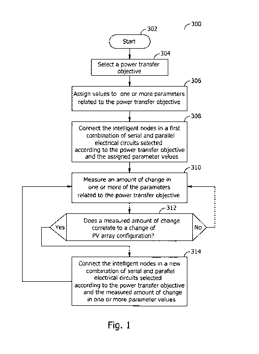
[0012] FIG. 1 is a block diagram illustrating steps in an example of a method
in accord with the
present invention.
[0013] FIG. 2 is a schematic diagram of an example of a photovoltaic panel
referred to herein as
an intelligent node. The intelligent node example of FIG. 2 is adapted for
selectable serial or
parallel electrical connections with other intelligent nodes, includes a
bypass circuit, and is further
-4-
CA 02751063 2011-07-28
WO 2010/087804 PCT/US2009/002683
adapted for exchange of data and commands with other intelligent nodes and
with a central control
and monitoring computer system.
[0014] FIG. 3 is a simplified schematic diagram of an integer number "n" of
the intelligent
nodes of FIG. 2 interconnected with cable assemblies in a serial electrical
circuit.
[0015] FIG. 4 is a simplified schematic diagram of an integer number "n" of
the intelligent
nodes of FIG. 2 interconnected with cable assemblies in a parallel electrical
circuit.
[0016] FIG. 5 is a simplified schematic diagram of an example of a simple PV
array having
three of the intelligent nodes of FIG. 2 interconnected with serial and
parallel electrical connections.
[0017] FIG. 6 is a schematic diagram of an example of a PV array having twelve
of the
intelligent nodes of FIG. 2 in an electrical circuit with an inverter and an
electrical load. The
electrical load in the example of FIG. 6 is representative of an electrical
load whose impedance
ZLOAD changes during operation of the PV array. The PV array example of FIG. 6
may be
selectively configured as in any of the examples of FIG. 7-12 according to
settings chosen for
series-parallel selectors X1-X12.
[0018] FIG. 7 is a schematic diagram for an example of one of many possible
selectable
electrical configurations for the PV array example of FIG. 6. In the example
of FIG. 7, all of the
intelligent nodes in the PV array are electrically connected in parallel.
[0019] FIG. 8 is a schematic diagram showing the PV array example of FIG. 6
configured as
two groups of intelligent nodes electrically connected in series, with six
intelligent nodes
electrically connected in parallel in each group.
[0020] FIG. 9 is a schematic diagram showing the PV array example of FIG. 6
configured as
three groups of intelligent nodes electrically connected in series, with four
intelligent nodes
electrically connected in parallel in each group.
[0021] FIG. 10 is a schematic diagram showing the PV array example of FIG. 6
configured as
four groups of intelligent nodes electrically connected in series, with three
intelligent nodes
electrically connected in parallel in each group.
-5-
CA 02751063 2011-07-28
WO 2010/087804 PCT/US2009/002683
[0022] FIG. 11 is a schematic diagram showing the PV array example of FIG. 6
configured as
six groups of intelligent nodes electrically connected in series, with two
intelligent nodes
electrically connected in parallel in each group.
[0023] FIG. 12 is a schematic diagram showing the PV array example of FIG. 6
with all of the
intelligent nodes electrically connected in series.
[0024] FIG. 13 is an example of a variation of the method of FIG. 1. In the
example of FIG. 13,
steps are shown for a power transfer objective of maintaining configurable PV
array output voltage
within the DC voltage input range for a DC-to-AC inverter.
[0025] FIG. 14 is an example of another variation of the method of FIG. 1. In
the example of
FIG. 14, steps are shown for a power transfer objective of equalizing the
impedance of the
configurable PV array and the impedance of an electrical load equal.
[0026] FIG. 15 is a first part of an example of another variation of the
method of FIG. 1. In the
example of FIG. 15, steps are shown for a power transfer objective of
operating the configurable PV
array at the maximum power point (MPP).
[0027] FIG. 16 is a continuation of the example of FIG. 15.
DESCRIPTION
[0028] A method is provided for efficiently transferring electrical power from
a photovoltaic
(PV) array to an electrical load connected to the PV array by configuring
connections between PV
panels in the PV array in selectable combinations of serial and parallel
electrical circuits. In related
variations of the disclosed method, power is transferred according a selected
power transfer
objective. A power transfer objective is a target, guideline, or principle for
determining a preferred
electrical configuration of a PV array. In some cases, a power transfer
objective is not fully
attainable but may be approached by an optimum selection of PV array
parameters. For example, in
one variation, the power transfer objective is to maintain a value of output
voltage from the
configurable PV array within the limiting values of a DC input range
specification for a DC to AC
inverter. In another variation, the power transfer objective is to transfer
power from the PV array to
the electrical load at the maximum power point (MPP). In another variation,
the power transfer
objective is to cause the impedance of the PV array and the impedance of the
electrical load to
differ by less than a specified maximum amount of error. In yet another
variation, the power
-6-
CA 02751063 2011-07-28
WO 2010/087804 PCT/US2009/002683
transfer objective is to rapidly adapt a PV array to changes in incident
illumination, temperature, or
other specified parameters. Other variations of the method seek optimizations
based on a
combination of power transfer objectives.
[0029] Examples of a PV panel suitable for use with the examples disclosed
herein are
referred to as intelligent nodes. Examples of intelligent nodes are described
in U.S. Patent
Application serial number 12/243,890, filed October 1, 2008 with the title
"Network Topology for
Monitoring and Controlling a Solar Panel Array", incorporated herein by
reference, and U.S. Patent
Application serial number 12/352,510, filed January 12, 2009 with the title
"System for Controlling
Power From A Photovoltaic Array By Selectively Configuring Connections Between
Photovoltaic
Panels", incorporated herein by reference.
[0030] Advantages of the disclosed method include economical and efficient
control of
power transfer from PV arrays of fewer than a hundred PV panels to utility-
scale PV arrays with
hundreds of thousands of PV panels. Another advantage is rapid reconfiguration
of serial and
parallel electrical connections for adapting a PV array to changes in
operating conditions. For
example, in a PV array having 100,000 intelligent nodes communicating with a
central monitoring
and control computer by a relatively slow wireless link, electrical
connections to every panel in the
array could be electrically switched to a new configuration in less than five
minutes. In many cases,
a change in configuration will not require a change in connections to every
panel, so even with a
relatively slow communications link to PV panels in the PV array,
configuration changes would
generally be fast enough to track many transient phenomena encountered during
PV array
operation. It is therefore practical to reconfigure a PV array by the
disclosed method in response to
moving cloud shadows, shadows from structures that change position as the sun
changes position in
the sky, changes in electrical load, weather changes, PV panel failures, PV
panel maintenance, and
so on. Furthermore, in a large PV array, much of the data sent to individual
PV panels would travel
over relatively high speed data pathways, reducing time needed for
reconfiguring the array from a
few minutes to a few seconds.
[0031] In some variations of the method, the larger the PV array, the more
closely outputs
from the PV can be made to approach conditions related to a selected power
transfer objective. For
example, in some variations of the method, the larger the PV array, the more
closely the impedance
of the PV array can be made to approach the impedance of an electrical load
receiving power from
the array. In other variations, the larger the PV array, the more closely the
PV array can be made to
approach a changed value of MPP related to a change in operating temperature
or incident
-7-
CA 02751063 2011-07-28
WO 2010/087804 PCT/US2009/002683
illumination. Other advantages include formation of serial and parallel
electrical connections
between PV panels in a PV array without exposing semiconductor components to
high voltage or
high current and elimination of some electrical equipment having the potential
to cause a single
point failure. Improved system reliability compared to PV power generation
systems known in the
art is another advantage. Furthermore, the disclosed method may be followed
during normal
operation of a PV array, that is, the array can be reconfigured from one
combination of serial and
parallel connections to another without disconnecting and reconnecting
electrical cables. Another
advantage is improving the efficiency of power transfer from a PV array to an
electrical load
receiving power from the array.
[0032] An example of a method in accord with the invention is shown in FIG. 1.
The
example of the method 300 in FIG. 1 begins at step 302. In step 304, a power
transfer objective for
power output by a configurable PV array to an electrical load is selected.
Subsequent steps in the
method depend on parameters and conditions related to the selected power
transfer objective.
[0033] The example of the method 300 in FIG. 1 continues with step 306, in
which values
are assigned to parameters related to the power transfer objective. Values may
optionally be
assigned by measurement of parameter values, for example, but not limited to,
configurable PV
array output voltage, configurable PV array output current, PV array
impedance, electrical load
impedance, average value of illumination incident on intelligent nodes in the
configurable PV array,
or other selected parameters. Alternatively, parameter values may be assigned
as the result of
calculations using target values related to reference conditions for
illumination, temperature, load
impedance, or other selected parameters related to a power transfer objective.
Or, some parameters
may be assigned values by calculation and other parameters may be assigned
values by
measurement.
[0034] Next, in step 308, a first combination of serial and parallel
electrical connections
between intelligent nodes is selected according to the power transfer
objective selected in step 304
and the parameter values assigned in step 306. The first combination of serial
and parallel
connections is referred to herein as a baseline configuration for the
configurable PV array.
Variations in parameter values related to the power transfer objective
optionally result in the PV
array being changed from the baseline configuration to a new configuration. In
step 308, after
selecting a combination of serial and parallel connections between intelligent
nodes, the intelligent
nodes are electrically interconnected according to the selected combination.
-8-
CA 02751063 2011-07-28
WO 2010/087804 PCT/US2009/002683
[0035] In step 310, an amount of change is measured for one or more parameters
related to
the power transfer objective. For example, in some variations of the method,
load impedances are
measured at different times and an amount of change in load impedance is
determined. Then, in
step 312, the measured amount of change is evaluated to determine if the
configuration of the PV
array should be changed. If the amount of change in a parameter correlates
more closely with a new
PV array configuration than with the current PV array configuration, then in
step 314, connections
between the intelligent nodes are reconfigured according to the new PV array
configuration related
to the changed parameter values from step 312. If the amount of change in one
or more parameters
does not correlate to a new PV array configuration, the method returns to step
310 to measure new
values for one or more parameters. One will appreciate that, although no
explicit termination step is
shown for the example of a method 300 illustrated in FIG. 1, the method may
optionally be
interrupted at any selected step.
(0036] Methods in accord with the invention are directed at a configurable PV
array which
includes two or more intelligent nodes. A circuit diagram for an example of an
intelligent node is
shown in FIG. 2, which is a representation of the intelligent node disclosed
in Application Serial
No. 12/352,510, wherein the intelligent node is referred to as a configurable
PV panel, and the
communications, monitoring, and control features disclosed for an intelligent
node in Application
Serial No. 12/243,890. The intelligent node 100 of FIG. 2 includes a PV module
108 for generating
electrical power from solar radiation, a node controller 114 for monitoring
and controlling the
intelligent node 100, and an electrically controlled bypass selector 120 for
selectively excluding
current and voltage output from the PV module 108 from current and voltage on
a first power
connector P1 102. The intelligent node 100 of FIG. 2 further includes a second
power connector P2
156 and an electrically controlled series-parallel selector Xn 138 for
selectively connecting to other
intelligent nodes 100 with serial electrical connections, parallel electrical
connections, or a
combination of serial and parallel electrical connections.
[0037] The intelligent node 100 of FIG. 2 includes a node controller 114
adapted for
communication with other nodes, a gateway, or a central monitoring and control
computer. A node
controller may include, for example but not limited to, an electrical circuit
comprising a plurality of
discrete circuit components, a programmable logic array, a gate array, an
application-specific
integrated circuit, or a microprocessor or microcontroller with associated
support circuits. A
gateway is an optional network communications device which collects data from
a group of
intelligent nodes before forwarding the data to the central monitoring and
control computer. Also,
-9-
CA 02751063 2011-07-28
WO 2010/087804 PCT/US2009/002683
commands received from the central monitoring and control computer are
optionally distributed to
the group of intelligent nodes by the gateway.
[0038] The node controller 114 of FIG. 2 transmits and receives data and
commands by any
of several redundant means of communication. More than one means of
communication may
optionally be used to exchange data and commands with other equipment. For
example, the
intelligent node may optionally be equipped with a control and monitoring
interface connector P3
162 electrically connected to the node controller 114 by a plurality of
electrical lines 164 for wired
communications with other equipment. The intelligent node may optionally
include a power line
communication interface (PLC I/F) 182 electrically connected to a
bidirectional communication
port of the node controller 114 and electrically coupled through circuitry
included in the PLC
interface 182 to connector P2 156. A wireless transceiver (XCVR) 180 may also
optionally be
provided for exchange of data and commands. The wireless XCVR 180 is
electrically connected to
a bidirectional communication port on the node controller 114 and exchanges
signals representative
of data and commands with other wireless transceivers, for example wireless
transceivers in other
intelligent nodes or gateways. Under some circumstances, for example when a
gateway is not in
operation, an intelligent node may optionally exchange data and commands by
wireless
communication with a central monitoring and control computer. A wireless
transceiver 180 adapted
for short range communication, for example a Bluetooth transceiver, may be
included in the
intelligent node 100. Alternatively, a transceiver for long range
communication may be included,
for example a Wifi transceiver or a transceiver using other wireless
communication technology.
[0039] The node controller 114 in FIG. 2 monitors parameters related to the
performance of
the PV module 108 and intelligent node 100 and sets a switching state of the
bypass selector 120
and a separate switching state of the series-parallel selector Xn 138.
Examples of parameters
monitored by the node controller include, but are not limited to, PV module
108 output current,
measured by a current measurement circuit 174, PV module 108 output voltage,
measured by a
voltage measurement circuit 176, one or more PV module temperatures, measured
by one or more
temperature measurement circuits 178, azimuth and elevation angles of the PV
module 108, current
and voltage on the second power connector P2 156, and current and voltage on
the first power
connector P1 102. The node controller 114 may optionally be configured to
detect electrical fault
conditions within the PV module 108 or the intelligent node 100, partial
shading of the PV module
108, reductions in electrical power from precipitation, dust, or debris on a
surface of the PV module
108, and reductions in incident radiation from dust in the air, precipitation,
or cloud cover. The
-10-
CA 02751063 2011-07-28
WO 2010/087804 PCT/US2009/002683
node controller 114 may also optionally be configured to monitor other sensors
such as sensors for
monitoring PV module surface reflectivity, incident light intensity, PV module
azimuth and
elevation angles, and may be adapted to control actuators such as azimuth and
elevation motors for
tracking the sun's position.
[0040] Switching states for the electrically controlled bypass selector 120
and the
electrically controlled series-parallel selector Xn 138 determine how current
and voltage output
from the PV module 108 is combined with electrical power flowing through the
first and second
power connectors P1 102 and P2 156. As shown in FIG. 2, the bypass selector
120 and the series-
parallel selector Xn 138 are preferably double-pole, double-throw (DPDT)
electromechanical
relays. Either one or both of the selectors (120, 138) may alternatively be
replaced by a solid state
relay or solid state switching devices made from discrete electronic
components. Either selector
(120, 138) may optionally be changed from a single DPDT electrically
controlled switching device
to a pair of single-pole, single-throw switching devices sharing a common
control line electrically
connected to the node controller 114.
[0041] Referring to FIG. 2, electric power from other intelligent nodes in a
configurable PV
array may optionally be connected to the intelligent node 100 on the second
power connector P2
156 comprising a first terminal 158 and a second terminal 160. Voltage and
current on the P2 first
terminal 158 and the P2 second terminal 160 are selectively combined with
voltage and current
output from the PV module 108 according to selected switching states for the
bypass selector 120
and the series-parallel selector Xn 138 as will be explained later. The P2
first terminal 158 is
electrically connected to a parallel terminal 144 of a first S-P switch 140 in
the series-parallel
selector Xn 138. The P2 first terminal 158 is further electrically connected
to a series terminal 154
of a second S-P switch 148 in the series-parallel selector Xn 138. The P2
second terminal 160 is
electrically connected to a parallel terminal 152 of the second S-P switch
148.
[0042] A series terminal 146 of the first S-P switch 140 is electrically
connected to a
common terminal 128 for a first bypass switch 122 in the bypass selector 120.
A common terminal
142 of the first S-P switch 140 is electrically connected to a common terminal
132 for a second
bypass switch 130 in the bypass selector 120. The common terminal 142 of the
first S-P switch 140
is further connected electrically to a connector PI first terminal 104. A
common terminal 150 of the
second S-P switch 148 is electrically connected to a negative terminal 112 on
the PV module 108,
to a connector P1 second terminal 106, and to a bypass terminal 126 of the
first bypass switch 122
in the bypass selector 120.
-11-
CA 02751063 2011-07-28
WO 2010/087804 PCT/US2009/002683
[0043] Continuing with FIG. 2, a positive terminal 110 of the PV module 108 is
connected
electrically to an input of the current measurement circuit 174. An output of
the current
measurement circuit 174 is electrically connected to a normal terminal 134 of
the second bypass
switch 130 in the bypass selector 120. A bypass selector control line 118
carries control signals
from the node controller 114 to a control input of the bypass selector 120. A
first control signal
from the node controller 114 on the bypass selector control line 118 sets the
bypass selector 120 to a
"Bypass" switching state in which output from the PV module 108 is excluded
from the voltage and
current on the terminals of the first power connector P1 102. A "Bypass"
switching state is also
referred to herein as a "B" switching state. A second control signal from the
node controller 114 on
the bypass selector control line 118 sets the bypass selector 120 to a
"Normal" switching state in
which output from the PV module 108 is selectively combined with the voltage
and current on the
terminals of the connector PI 102 according to one of two alternate switching
states for the series-
parallel selector Xn 138. A "Normal" switching state is also referred to
herein as an "N" switching
state. In the example of FIG. 2, the first bypass switch 122 and the second
bypass switch 130 in the
bypass selector 120 are shown in the "Normal" switching state. FIG. 2 further
shows the first
bypass switch 122 normal terminal 124 and the second bypass switch 130 bypass
terminal 136 as
unterminated. One skilled in the art will appreciate that passive components
may optionally be
electrically connected to the unterminated terminals to reduce an amount of
noise coupled into the
circuit.
[0044] A series-parallel selector control line 116 carries control signals
from the node
controller 114 to a control input of the series-parallel selector Xn 138. A
third control signal from
the node controller 114 on the series-parallel selector control line 116 sets
the series-parallel
selector Xn 138 to a "Series" switching state, also referred to herein as an
"S" switching state. A
fourth control signal from the node controller 114 on the series-parallel
selector control line 116 sets
the series-parallel selector Xn 138 to a "Parallel" switching state, also
referred to herein as a "P"
switching state. In the example of FIG. 2, the first S-P switch 140 and the
second S-P switch 148 in
the series-parallel selector Xn 138 are shown in the "Series" switching state.
[0045] FIG. 3 illustrates an example of a configurable PV array having an
integer number
"n" of intelligent nodes 100 electrically connected in series by cable
assemblies 166. As shown in
FIG. 3, series-parallel selectors (138 X1, 138 X2, ... 138 Xn) are shown in an
"S" switching state.
All of the bypass selectors 120 in the "n" number of panels are set to an "N"
switching state in the
example of FIG. 3. An output voltage Vout from the PV array, measured from a
PV array negative
-12-
CA 02751063 2011-07-28
WO 2010/087804 PCT/US2009/002683
output terminal 170 to a PV array positive output terminal 168, is the sum of
the output voltages of
the "n" intelligent nodes. In the configuration shown in FIG. 3, an output
voltage for the
configurable PV array further corresponds to the PV array output voltage Vout
measured from a
connector P2 terminal 1 158 in intelligent node number "n" to a connector P1
terminal 1 104 in
intelligent node number 1. In the case of an intelligent node having the
series-parallel selector set to
the "S" state and the bypass selector 120 set to the "B" state, output voltage
from the intelligent
node's PV module is excluded from the output voltage Vout by a circuit path in
the intelligent node
around the PV module between the first power connector P1 and the second power
connector P2.
[0046] FIG. 4 illustrates one of many alternative electrical configurations
for the "n"
number of intelligent nodes electrically connected to form a configurable PV
array in the example
of FIG. 2. In FIG. 4, an integer number "n" of intelligent nodes 100 are
electrically interconnected
by cable assemblies 166 in a parallel electrical configuration with series-
parallel selectors (138 X1,
138 X2, ... 138 Xn) in a "P" switching state. Bypass selectors 120 are shown
in an "N" switching
state. An output voltage Vout from the configurable PV array, measured from a
PV array negative
output terminal 170 to a PV array positive output terminal 168, is equal to an
output voltage from
any one of the intelligent nodes 100 all of which, for purposes of this
example, have equal output
voltages. In the case of intelligent nodes having different output voltages, a
PV array output voltage
may be calculated by conventional methods for analyzing parallel electrical
circuits. An output
current from the configurable PV array example of FIG. 4 is equal to the
arithmetic sum of the
current output from each of the "n" number of intelligent nodes, an optional
current input to
connector P1 on intelligent node 100 number 1, and an optional current input
to connector P2 on
intelligent node 100 number "n". PV array negative output terminal 170 may
alternately be
electrically connected to connector P2 terminal 2 160 on intelligent node 100
number "n" or to
connector P1 terminal 2 106 on intelligent node 100 number 1, as indicated by
dashed connection
lines in FIG. 4. PV array positive output terminal 168 may alternately be
electrically connected to
connector PI terminal 1 104 on intelligent node number 1 or to connector P2
terminal 1 158 on
intelligent node number "n", as indicated by dashed connection lines in FIG.
4.
[0047] FIG. 5 shows an example of a configurable PV array including three
intelligent
nodes connected in a combination of serial and parallel electrical
connections. In the example of
FIG. 5, intelligent node 100 number 1 has a series-parallel selector 138 X1
set to a "P" switching
state. The series-parallel selector 138 X2 in intelligent node 100 number 2 is
in an "S" switching
state, and intelligent node number 3 has a series-parallel selector 138 X3 set
to an "S" switching
-13-
CA 02751063 2011-07-28
WO 2010/087804 PCT/US2009/002683
state. A PV array output voltage Vout measured between the PV array positive
output terminal 168
and the PV array negative output terminal 170 in FIG. 5 is approximately twice
the PV array output
voltage for intelligent nodes connected in parallel as shown in the example of
FIG. 4. A PV array
configured as in FIG. 5 will therefore produce an output voltage that is
greater than or equal to the
minimum input voltage for an inverter under lower levels of illumination than
the PV array example
of FIG. 4. A configurable PV array having selectable serial and parallel
connections between
intelligent nodes, as in the example of FIG. 5, captures electrical power for
output to an electric
power grid under conditions in which intelligent nodes interconnected only in
parallel output power
at too low a voltage for connection to an inverter input.
[0048] The example of FIG. 6 may be used to illustrate examples of
combinations of serial
and parallel electrical connections and corresponding configurable PV array
output voltages
produced by a configurable PV array having twelve intelligent nodes. FIG. 6
further illustrates an
example of an electrical load connected to the configurable PV array, wherein
the electrical load has
impedance which may vary with time, and a monitoring and control computer
system adapted to
receive a signal related to load impedance. The monitoring and control
computer system may
optionally use the value of load impedance to select a combination of serial
and parallel connections
in the configurable PV array, or the combination may be selected by an
intelligent node designated
for the purpose.
[0049] Differences in output voltages between any two configurations of the
configurable
PV array correspond to differences in PV array impedance, as previously
explained. An output
voltage Vout from the configurable PV array is measured across a PV array
positive output terminal
168 and a PV array negative output terminal 170. Connector P1 terminal 1 104
on intelligent node
100 number 1 is electrically connected to PV array positive output terminal
168, which is further
electrically connected to a first DC input on an inverter 172. Connector P2
terminal 1 158 on
intelligent node 100 number 12 is electrically connected to PV array negative
output terminal 170,
which is further electrically connected to a second DC input on the inverter
172. Each of the
intelligent nodes 100 represented in simplified form in FIG. 6 includes a PV
module 108 and a
series-parallel selector (X1, X2, X3, ... X12).
[0050] In a first alternative configuration illustrated in the simplified
equivalent electrical
circuit of FIG. 7, the twelve intelligent nodes of the example of FIG. 6,
represented in FIG. 7 by PV
modules 108, are connected in a parallel electrical circuit. An output voltage
from a PV module
108, measured across a positive terminal 110 and a negative terminal 112, is
represented by a
-14-
CA 02751063 2011-07-28
WO 2010/087804 PCT/US2009/002683
voltage "E". For the parallel electrical configuration of FIG. 7,
corresponding to a "P" switching
state selected for all twelve series-parallel selectors (X1-X12), the output
voltage Vout of the
configurable PV array, measured across the first and second output terminals
(168, 170) is equal to
"E".
[0051] Table 1 summarizes the switching states for the twelve series-parallel
selectors in the
examples of FIGS. 6-12.
Table 1. "S" and "P" switching states corresponding to PV array output voltage
Vout.
FIG. X1 X2 X3 X4 X5 X6 X7 X8 X9 X10 X11 X12 Vout
6 P P P P P P P P P P P P E
7 P P P P P S P P P P P S 2E
8 P P P S P P P S P P P S 3E
9 P P S P P S P P S P P S 4E
P S P S P S P S P S P S 6E
11 S S S S S S S S S S S S 12E
[0052] FIGS. 8 - 12 illustrate more alternative electrical configurations for
the example of
FIG. 6. FIG. 8 shows an equivalent electrical circuit for two serially
connected groups with six
intelligent nodes connected in parallel in each group. The PV array
configuration of FIG. 8 has an
output voltage across the first and second PV array output terminals (168,
170) of 2 x E, where "E"
is defined as for FIG. 7. Switch states for the twelve series-parallel
selectors in the PV array are
shown in Table 1.
[0053] FIG. 9 shows an equivalent electrical circuit for three serially
connected groups with
four intelligent nodes connected in parallel per group and a PV array output
voltage Vout equal to 3
x E. FIG. 10 shows four serially connected groups having three intelligent
nodes in parallel per
group and a PV array output voltage of 4 x E. A PV array output voltage Vout
equal to 6 x E is
achieved by the configuration illustrated in FIG. 11, which shows six serially
connected groups,
-15-
CA 02751063 2011-07-28
WO 2010/087804 PCT/US2009/002683
each group having two intelligent nodes in parallel. Lastly, FIG. 12 shows a
configuration having
the maximum value of PV array output voltage. In FIG. 12, all twelve
intelligent nodes are
connected in series.
[0054] The examples of FIGS. 6 to 12 may be extended to very large
configurable PV
arrays comprising many hundreds or even many thousands of intelligent nodes.
In some very large
configurable PV arrays, an inverter having a high value for minimum DC input
voltage is preferred.
For example, in one example of a grid-connected inverter known in the art, the
minimum DC input
voltage is approximately fifteen times the voltage output from a single
intelligent node. That is, at
least fifteen intelligent nodes are electrically connected in series to
generate an output voltage large
enough to input to the inverter. In such a case, a configurable PV array has
many serially connected
chains of intelligent nodes with the chains of intelligent nodes further
connected in parallel to one
another and to the inputs of an inverter.
[0055] Embodiments of the invention are suitable for use in very large PV
arrays
comprising a plurality of series-connected chains of configurable PV panels in
a parallel electrical
circuit. Operation of an embodiment in a large array may be compared to the
operation in the
examples described previously herein by substituting a serially connected
chain of configurable PV
panels for a single panel in an example. For example, each of the intelligent
nodes in the examples
of FIGS. 6 to 12, represented in the figures by a PV module 108, could
optionally be replaced by a
serially connected chain of intelligent nodes to model the behavior of a very
large number of
intelligent nodes in a PV array supplying power to an inverter with a high
minimum input voltage.
[0056] Connections between intelligent nodes adapted for connection to other
intelligent
nodes as described in the previous examples may be selectively configured
according to different
power transfer objectives. Examples of variations in the method of FIG. 1 are
shown in FIGS. 13-
16. FIG. 13 illustrates a variation in which the power transfer objective is
to maintain a value for
the configurable PV array output voltage within the DC voltage input range for
a DC-to-AC
inverter. FIG. 14 illustrates a variation in which the power transfer
objective is to equalize source
impedance and load impedance, where source impedance corresponds to PV array
impedance, and
load impedance. FIGS. 15-16 illustrate steps in a variation of the method in
which the power
transfer objective is to operate a configurable PV array at the MPP.
[0057] FIG. 13 illustrates an example of a variation of the method of FIG. 1
in which the
selected power transfer objective is to generate a magnitude of PV array
output voltage that is
-16-
CA 02751063 2011-07-28
WO 2010/087804 PCT/US2009/002683
greater than or equal to the minimum DC input voltage for a DC to AC inverter
and less than or
equal to the maximum DC input voltage for the inverter. Numeric labels
assigned to the steps in
FIG. 13 indicate the corresponding steps shown in FIG. 1. The example of FIG.
13 begins at step
302 and proceeds to step 304, in which the power transfer method is selected.
Such a selection may
be implemented, for example, by presenting to a person responsible for
managing a photovoltaic
power generation system different options for power transfer objectives on a
display device that is
part of a central monitoring and control computer system.
[0058] In the example of FIG. 13, step 306 from FIG. 1 is shown to include
steps 306-1 to
306-4. In step 306-1, a table of PV array output voltage values is calculated.
Each entry in the table
is related to an output voltage from a selected combination of serial and
parallel electrical
connections between intelligent nodes in a configurable PV array. In step 306-
2, values are
obtained for a minimum value and a maximum value for DC-to-AC inverter input
voltage. The
minimum and maximum input voltage values together define a DC input voltage
range for the
inverter.
[0059] One skilled in the art will understand that an inverter outputs AC
voltage within a
specified voltage range when a voltage value for electrical power input to the
inverter is within the
inverter's specified DC input voltage range. If input voltage is outside the
specified input range, it
may be necessary to disconnect an electrical load receiving power from the
inverter outputs. For
example, when an amount of illumination incident on a PV array decreases as a
result of the sun's
daily motion, the output voltage from a PV array will eventually fall below
the minimum input
voltage for an inverter. Subsequent power output from the array is wasted
until illumination levels
increase enough to generate power having a sufficient magnitude of voltage for
supplying the
inverter. A configurable PV array may therefore capture power that would be
wasted by a PV array
known in the art by reconfiguring serial and parallel electrical connections
between intelligent
nodes to increase the magnitude of output voltage from the array.
[0060] Continuing with FIG. 13, in step 306-3, a baseline configuration is
selected for the
configurable PV array. The baseline configuration in the example of FIG. 13
corresponds to a
configuration having an output voltage determined in step 306-1 that is within
the DC input voltage
range for the inverter. In step 306-4, the table of values calculated in step
306-1 is optionally
normalized to the value of output from the baseline configuration.
Normalization is useful for
quickly selecting a new PV array configuration that correlates to an amount of
change in the PV
array output voltage. Normalization and other calculations in the variations
of the method described
-17-
CA 02751063 2011-07-28
WO 2010/087804 PCT/US2009/002683
herein may alternatively be performed by the central monitoring and control
computer system or by
an intelligent node designated for the purpose.
[0061] The array of intelligent nodes is switched into the selected
combination of serial and
parallel connections in step 308. In step 310, the output voltage of the
configurable PV array is
measured again, and an amount of change from the previously measured value is
calculated. In step
312, the amount of change in output voltage is compared to the minimum and
maximum values for
the inverter input range. If the new value of output voltage is outside the
inverter input range, a new
PV array configuration is selected to restore the output voltage to a value
within the inverter input
range. In step 314, the intelligent nodes in the configurable PV array are
switched to the newly
selected configuration. If instead the voltage from step 310 is still within
the inverter input range,
then step 312 returns to step 310 without changing the PV array configuration.
The method
illustrated in FIG. 13 is operative until all the intelligent nodes in the
configurable PV array are
electrically connected in series.
[0062] In FIG. 14, another example of a power transfer objective is to
equalize source (i.e.,
configurable PV array) impedance and electrical load impedance. The power
transfer objective in
the variation of the method shown in FIG. 14 is related to the engineering
principle that a maximum
amount of electrical power may be transferred from a power source, for example
a photovoltaic
array, to an electrical load, for example the combination of an AC load and a
DC-to-AC inverter
supplying power to the AC load, when the impedance of the electrical load and
the impedance of
the power source are equal.
[0063] In general, impedance Z is related to resistance R and frequency ^ by
the well-
known relationship in equation (1):
(1) Z = R + i ^
For the photovoltaic cells in an intelligent node, the real term (R) in
equation (1) predominates and
the imaginary term (i ^) may be ignored. The impedance Z of the PV module in
an intelligent node
may therefore be approximated by the combined resistances of the PV cells in
the intelligent node,
determined using Ohm's Law and measured values for the current output and
voltage output for the
DC power output from the intelligent node. The impedance Z for a PV array
having many
interconnected intelligent nodes may similarly be found by Ohm's Law using
values for the output
voltage E from the array and the output current I from the array as in
equation (2):
-18-
CA 02751063 2011-07-28
WO 2010/087804 PCT/US2009/002683
(2) ZzR=E/I
For a selected value of current I, changes in the impedance of a PV array made
to match PV array
impedance with load impedance are related to changes in the output voltage E
of the PV array. As
an example, FIGS. 7-12 are each labeled with a value "Zr" of impedance
determined by equation 2
for each of the serial-parallel configurations shown, relative to the
impedance of the PV array in
FIG. 7 (12 PV panels connected in parallel). Values of Zr range from Zr=1 in
FIG. 7 to Zr = 12 in
FIG. 12. A method for adjusting PV array impedance is therefore based on
selecting the
combination of serial and parallel connections between intelligent nodes in a
PV array that results in
a discrete magnitude of change in PV array output voltage that is within a
predictable maximum
error of the magnitude of change in the impedance of an electrical load
receiving power from the
PV array.
[0064] FIG. 14 represents a variation of the method illustrated in FIG. 1.
Numeric labels
assigned to the steps in FIG. 14 indicate the corresponding steps in FIG. 1.
In FIG. 14, the example
of a method in accord with the invention begins with step 302. Next, in step
304, a power transfer
objective is selected. The power transfer objective shown for the example of
FIG. 13 is
equalization of source impedance, i.e. PV array impedance, and load impedance.
[0065] Next, in steps 306-1 to 306-4, parameters related to the power transfer
objective are
assigned values. In step 306-1, a table of values of discrete changes in
output voltage is calculated.
The discrete changes in output voltage correspond to discrete changes in PV
array impedance that
may be selected for a configurable PV array.
[0066] Table 2 lists some of the discrete steps in PV array impedance, related
to discrete
steps in PV array output voltage as previously described, that can be produced
by an example of a
configurable PV array having 96 intelligent nodes. Table 2 shows the
permutations of serial-
parallel circuits that can be made from 96 intelligent nodes arranged into "J"
groups of intelligent
nodes, each group having "K" number of intelligent nodes in parallel and "J"
number of groups
electrically connected in series. The quantity Vs in Table 2 refers to the
output voltage from one
intelligent node. For the purposes of this example, Vs is the same for all the
intelligent nodes in the
configurable PV array.
[0067] Table 2. Discrete steps in output voltage from an example of a
configurable PV
array with 96 intelligent nodes.
-19-
CA 02751063 2011-07-28
WO 2010/087804 PCT/US2009/002683
No. of Serially- No. of Intelligent Impedance of PV Normalized to Z for
Connected Groups, J Nodes Connected in Array, Z J=12 and K=8
Parallel In Each
Group, K
1 96 1 0.08
2 48 2 0.17
3 32 3 0.25
4 24 4 0.33
6 16 6 0.50
8 12 8 0.67
12 8 12 1.0
16 6 16 1.3
24 4 24 2.0
32 3 32 2.7
48 2 48 4.0
96 1 96 8.0
The first data row in Table 2 refers to a single group of 96 intelligent nodes
electrically connected in
parallel, the second data row refers to two serially-connected groups with 48
intelligent nodes in
parallel in each group, and so on. The bottom row in Table 2 refers to all 96
intelligent nodes
electrically connected in series. The third column in Table 2, labeled
"Impedance of PV Array, Z"
refers to a value for array impedance relative to the impedance of an array
consisting of one
serially-connected group. Data in the third column of Table 2 is calculated
using conventional
methods for serial and parallel combinations of voltage sources, wherein the
PV modules in the
intelligent nodes correspond to the voltage sources. A difference between two
values in the third
column is related to a difference in impedance of the corresponding PV array
configurations.
-20-
CA 02751063 2011-07-28
WO 2010/087804 PCT/US2009/002683
[0068] Table 2 does not include all the combinations of serial and parallel
connections that
could be formed in a configurable PV array having 96 intelligent nodes. For
example, different
groups of intelligent nodes in a configurable PV array may optionally have
different numbers of
intelligent nodes connected in parallel in each group, thereby changing the
total number of groups
that may be connected in series, and correspondingly changing the discrete
intervals between
configurable PV array output voltages. Or, two or more intelligent nodes may
be placed in a
serially-connected group, and serially-connected groups may then be
interconnected in parallel.
Table 2 may readily be expanded to include all such configurations by
conventional calculation
methods for serial and parallel circuit combinations. Table 2 may also be
readily modified for
configurable PV arrays having different numbers of intelligent nodes,
including configurable PV
arrays having hundreds of thousands of intelligent nodes. In general, the
greater the number of
intelligent nodes in a configurable PV array, the smaller the size of an
incremental adjustment in
output voltage, or alternately in PV array impedance, that may be achieved by
reconfiguring serial
and parallel connections, and the finer the degree of control that may be
exercised in approaching a
power control objective. The magnitude of an incremental adjustment in output
voltage is related to
a maximum amount of error in achieving a power transfer objective.
[0069] The fourth column in Table 2 shows a value of PV array impedance
normalized to
the configuration for 12 serially-connected groups with 8 intelligent nodes in
parallel in each group.
The fourth column could optionally be normalized against any of the other data
rows in Table 2.
For example, under reference conditions for incident illumination,
temperature, and load
impedance, maximum power from a configurable PV array to an electrical load
may occur when the
array is configured as 12 serially-connected groups with 8 intelligent nodes
in parallel in each
group. As load impedance increases, for example a doubling of load impedance,
the configurable
PV array would be switched to a configuration with twice as much impedance as
the previous
configuration, corresponding to 24 serially connected groups with four
intelligent nodes in parallel
in each group as shown in Table 2.
[0070] After calculating a table of values related to changes in impedance for
selected
combinations of serial and parallel connections between intelligent nodes
(step 306-1 in FIG. 14), a
value for load impedance is obtained in step 306-2. Many power generation
systems, especially
large ones, have means for determining load impedance, and means for
communicating values for
load impedance to a central monitoring and control computer. A baseline
configuration for the PV
array is selected in step 306-3, for example by configuring the array for a
value of impedance
-21-
CA 02751063 2011-07-28
WO 2010/087804 PCT/US2009/002683
closest to the current value of load impedance. Next, in step 306-4, the table
of values related to
discrete PV array impedance changes calculated in step 306-1 is optionally
normalized to the
current PV array configuration, thereby making it easier to select a discrete
amount of increase or
decrease in impedance relative to the baseline configuration in response to
increases or decreases in
load impedance.
[0071] In step 308, the configurable PV array is switched into the combination
of serial and
parallel connections between intelligent nodes determined in steps 306-1 to
306-4. Next, in step
310, a new value of load impedance is obtained and a magnitude of change in
load impedance is
calculated. In step 312, a determination is made as to whether the magnitude
of change in load
impedance places the new load impedance closer to the current PV array
impedance or closer to the
PV array impedance corresponding to another array configuration. If the
magnitude of change in
impedance is large enough, the PV array configuration is changed to a new
configuration in step
314, otherwise the PV array configuration is left unchanged. That is, a
determination is made as to
whether the magnitude of change correlates more closely with the previous
array configuration or
with a new configuration. Another measurement and comparison cycle starts anew
at step 310.
[0072] In general, a discrete amount of impedance change resulting from a
change in serial
and parallel connections in the configurable PV array will not exactly equal
the amount of change in
load impedance. Alternative steps in the example of FIG. 14 may therefore
select either the next
highest step in output voltage or the next lowest step, as preferred for a
particular type of electrical
load or other operating consideration. Commands for changing the connections
between intelligent
nodes could alternatively be issued from the central monitoring and control
computer system or
from a designated intelligent node. Switching commands could optionally be
sent to all intelligent
nodes simultaneously or propagated peer-to-peer, that is, from intelligent
node to intelligent node.
[0073] FIG. 15 and FIG. 16 represent another variation of the method
illustrated in FIG. 1.
FIG. 16 is a continuation of the example from FIG. 15. The example of FIGS. 15-
16 illustrates
steps for implementing an example of a power transfer objective related to
operating the
configurable PV array at the maximum power point (MPP). Such a power transfer
objective is
useful, for example, for a configurable PV array supplying power to an
electrical load having a
relatively large input voltage range. In the method of FIGS. 15-16, the
configuration of the PV
array changes in response to changes in incident illumination, changes in
temperature, or other
changes that affect the current or voltage output of the PV array and
therefore cause a change in the
MPP.
-22-
CA 02751063 2011-07-28
WO 2010/087804 PCT/US2009/002683
[0074] In FIG. 15, the example begins with step 302. In step 304, a power
transfer objective
related to adapting the PV array configuration to track changes in MPP is
selected. In step 306-1, a
table of PV array output voltage values corresponding to selected PV array
configurations is
calculated. In step 306-2, a target value for configurable PV array output
current is assigned, for
example a target value related to array operation under specified conditions
of illumination,
temperature, and electrical load impedance. In step 306-3, values for MPP and
a voltage value
related to MPP at the target value of output current are determined. For
example, a value of MPP
may optionally be determined by maximizing the mathematical product of PV
array output current
from step 306-2 and a value of PV array output voltage under reference
conditions of illumination
and temperature, obtained from the table of step 306-1. In step 306-4, a
combination of serial and
parallel connections having an output voltage that gives a calculated output
power value closest to
the MPP value from step 306-3 is selected. In step 306-5, the table of PV
array output voltages
calculated in step 306-1 is optionally normalized to the array configuration
selected in step 306-4.
[0075] After step 306-5, the example of FIG. 15 continues in FIG. 16 at step
308, in which
the configurable PV array is switched into the combination of serial and
parallel connections
selected in step 306-4. Then, at step 310 in FIG. 16 a value of PV array
output current is measured.
A new value of MPP related to the new current value is calculated and compared
to the previously
determined MPP value in step 312. A determination is made in step 312 as to
whether the
magnitude of change in MPP impedance places the new MPP value closer to the
current PV array
configuration or closer to MPP calculated for the output voltage of another PV
array configuration.
If the magnitude of change in impedance is large enough, the PV array
configuration is changed to a
new configuration in step 314, otherwise the array configuration is left
unchanged. Another
measurement and comparison cycle starts anew at step 310.
[0076] One skilled in the art will appreciate that the method of FIG. 1 is
applicable to many
different power transfer objectives. For example, a power transfer objective
of finding the optimum
configuration of serial and parallel electrical connections between
intelligent nodes for simultaneous
changes in incident illumination and load impedance could be implemented by
finding the
configuration which most closely tracks a new value of MPP and at the same
time minimizes a
difference between source impedance and load impedance. Or, different power
transfer objectives
could be implemented sequentially in subsequent measurement and
reconfiguration cycles
(corresponding to steps 310-314 in FIG. 1). For example, a configurable PV
array could first be
-23-
CA 02751063 2011-07-28
WO 2010/087804 PCT/US2009/002683
configured to track MPP and next for matching source impedance and load
impedance, in a
repeating cycle.
[0077] Unless expressly stated otherwise herein, ordinary terms have their
corresponding
ordinary meanings within the respective contexts of their presentations, and
ordinary terms of art
have their corresponding regular meanings.
-24-