Note: Descriptions are shown in the official language in which they were submitted.
CA 02753992 2011-08-29
WO 2010/099831 1
PCT/EP2009/052683
Poly-phase reactive power compensator
Field of the invention
The invention relates to the field of reactive power
compensation, and in particular control of reactive power
compensators.
Background of the invention
As modern society relies heavily on a dependable power supply,
faults occurring in an electric power network have to be
remedied quickly. A single line to ground fault, or single
phase to ground fault, wherein one line to ground voltage
becomes depressed, is the most frequently occurring short-
circuit fault in the electrical power network.
A reactive power compensator, such as a static VAR compensator
(SVC) can be used to combat voltage fluctuations. The SVC
counteracts voltage drops in the electric power network by
providing reactive power and is often able to handle
overvoltages by absorbing reactive power. Today, there is a
desire to be able to use the SVC for voltage support also
during power network faults, and not only during steady state
and voltage recovery after fault clearance.
Summary of the invention
At the single phase to ground fault, the SVC provides equal
susceptance from all its phases, so called symmetrical
control. This may result in still low voltage in the faulted
phases and possibly excessive voltages in the non-faulted
phases as they also obtain a reactive power injection without
needing it. Such overvoltages may cause damage to network
devices and should obviously be avoided if possible.
CA 02753992 2011-08-29
WO 2010/099831 2
PCT/EP2009/052683
In view of the above, it would be desirable to provide means
for ensuring that undervoltages of faulted phases are
remedied, and also to avoid excessive voltages caused by
symmetrical control of the SVC during unsymmetrical power
network faults, such as single phase to ground faults.
It is an object of the invention to provide means for
improving the performance of a reactive power compensator
during single phase to ground faults in an electric power
network.
It is another object of the invention to provide means for
avoiding excessive voltages during unsymmetrical faults in an
electric power network, such as single phase to ground faults.
These objects, among others, are achieved by a poly-phase
reactive power compensator as claimed in the independent
claim.
In accordance with the invention a poly-phase reactive power
compensator is provided for providing reactive power to an
electric power network. The poly-phase reactive power
compensator comprises for each phase a reactive power means
for varying its susceptance. The poly-phase reactive power
compensator is characterized by means for transferring
susceptance between the reactive power means and thereby
between the phases. The invention provides a way of boosting
SVC output during unsymmetrical fault conditions.
In accordance with an embodiment of the invention, the means
for transferring susceptance comprises a thyristor switch
arrangement, which in turn comprises thyristor switches. A
simple, yet reliable and very fast arrangement for
accomplishing the power transfer is provided.
In accordance with another embodiment of the invention, the
susceptance means comprises thyristor-switched capacitors,
CA 02753992 2011-08-29
WO 2010/099831 3
PCT/EP2009/052683
each thyristor-switched capacitor in turn comprising a
capacitor bank and inductor in series connection with a
thyristor switch. By means of this feature, transfer of
thyristor-switched capacitors phases from non-faulted phases
to faulted phase is enabled. An optimized use of available
components is thus used, in that the thyristor-switched
capacitors, which would in most cases not be used for the non-
faulted phases during an unsymmetrical fault, are utilized. If
the thyristor-switched capacitors of the prior art solution
are utilized, they would all provide equal output, which would
still result in under-voltages of the faulted phase, and in
excessive voltages in the non-faulted phases. The invention
thus enables a way of ensuring that under-voltages of the
faulted phase are remedied by providing a novel unsymmetrical
control. Further, the invention also provides a way of
preventing excessive voltages.
In still another embodiment of the invention, the means for
transferring susceptance comprises a thyristor valve
arrangement. The thyristor valve arrangement comprises a set
of switches connected so as to enable the transfer of power
between the phases. Easily implemented power transfer means is
thereby provided.
In yet another embodiment of the invention, the reactive power
means comprises thyristor-controlled reactors, wherein each
thyristor-controlled reactor comprises an inductor in series
connection with a thyristor switch. By means of this feature,
large unsymmetrical transient overvoltages can be eliminated
or at least mitigated.
In yet another embodiment of the invention, the poly-phase
reactive power compensator comprises three phases, and the
reactive power means are connected in a delta-connection. The
CA 02753992 2015-10-06
4
invention can thus be implemented in existing reactive power
compensators.
In yet another embodiment of the invention, the poly-phase
reactive power compensator further comprises a control device
arranged to provide control orders to the thyristor switches in
dependence on need of the power network. The control of the
means of transferring susceptance between the phases can be
implemented in the control device used for controlling the
output from the reactive power compensator. Thus, no additional
components are required for implementing the invention.
In yet another embodiment of the invention, there is provided a
poly-phase reactive power compensator for providing susceptance
to an electric power network, said poly-phase reactive power
compensator comprising for each delta phase a reactive power
means for providing varying susceptance, characterized by means
for transferring susceptance between said reactive power means
and thereby between said phases, wherein said means for
transferring susceptance comprises a thyristor valve
arrangement, in turn comprising a first thyristor switch
connected at one end to a first phase and at the other end
between a thyristor switch and reactor of a third phase, a
second thyristor switch connected at one end to a second phase
and at the other end between the thyristor switch and reactor
of said first phase, and a third thyristor switch connected at
one end to said third phase and at the other end between the
thyristor switch and reactor of said second phase and, wherein
said reactive power means comprises thyristor-switched
capacitors, each thyristor-switched capacitor in turn comprising
CA 02753992 2015-10-06
4a
a capacitor bank and inductor in series connection with a
thyristor switch.
The invention also relates to a control device for controlling a
reactive power compensator.
Further features and advantages thereof will become clear upon
reading the following description and the drawings.
Brief description of the drawings
Figure 1 illustrates an SVC in accordance with the invention.
Figure 2a illustrates a delta-connected TSC arrangement.
Figure 2b illustrates a thyristor valve arrangement in
accordance with the invention.
Figure 3 illustrates the thyristor valve arrangement in
accordance with the invention in a second embodiment.
Detailed description of embodiments of the invention
The same reference numerals are used throughout the figures for
denoting the same or corresponding parts.
Figure 1 illustrates a reactive power compensator in accordance
with the invention, the reactive power compensator in the
following being exemplified by a static VAR compensator
CA 02753992 2011-08-29
WO 2010/099831 5
PCT/EP2009/052683
(SVC) 1. The SVC 1 comprises a number of thyristor-controlled
reactors 2 (TCR) and a number of thyristor switched capacitors
(TSC) 3. The SVC may further comprise one or more filter
device(s) 4. The TCR 2, the TSC 3, and the filter device 4 are
connected to an electric power network 5, denoted power
network in the following, via a medium voltage busbar (MVB) 6
and a transformer 7, both forming part of the SVC 1. The power
network 5 may for example be a three-phase electric ac
network.
In conventional manner, the TCR 2 comprises an inductor 8
connected in series with a controllable semiconductor device
9. The semiconductor device 9, in the following denoted
thyristor switch, comprises two stacks of thyristors in anti-
parallel connection. The TSC 3 comprises a current-limiting
inductor 15 and a capacitor bank 10 connected in series with a
thyristor switch 11. The filter device 4 comprises one or more
mutually parallel-connected filters, each filter being tuned
to resonance with a certain multiple of the nominal frequency
of the power network 5.
A control device 14 is connected to the SVC 1 for controlling
the TCR 2 and TSC 3. Voltages on the MVB 6 and in the power
network 5 are sensed in conventional manner and supplied to
the control device 14. The control device 14 then provides
control orders, indicated at Cl and C2, to the TCR 2 and TSC 3
in dependence on the measurements. The control orders Cl and
C2 comprises orders to the thyristor switches to be blocked or
unblocked, depending on the need for reactive power in the
power network 5.
At a single phase to ground fault, there is an under-voltage
in the faulted phase, the others may be unaffected, or also
have a somewhat low voltage or have high voltage. In
accordance with the invention, unsymmetrical control is used
CA 02753992 2011-08-29
WO 2010/099831 6
PCT/EP2009/052683
for combating the above-described problem. Unsymmetrical
control is used today in the sense that a single phase of the
SVC may be unblocked while the others are blocked, or that one
phase of the SVC is blocked, while the others are not, etc.
However, in the unsymmetrical control in accordance with the
invention, the surplus susceptance of the non-faulted phases
is used to improve the performance of the faulted phase.
In short, in a single-phase fault it is likely that not all
the TSCs will be used in all three phases during the power
network fault. There will thus be a deficit of susceptance in
the faulted phase and surplus in the other phases.
In accordance with the invention, a thyristor valve
arrangement is provided, by means of which transfer of TSC
phases from the non-faulted phase(s) to the faulted one is
enabled.
Figure 2a illustrates a conventional three-phase delta
arrangement comprising three TSCs 3a, 3b, 3c connected in a
delta connection. In particular, each TSC circuit 3a, 3b, 3c
comprises one arm of the delta arrangement and is connected
between two phases. The illustrated three phases are denoted
a, b and c. It is noted that the present invention may be
utilized for other types of connections as well, such as Y-
connected. However, the invention will be exemplified with the
illustrated conventional three-phase delta configured TSCs.
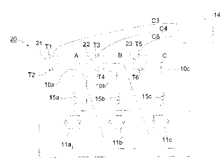
Figure 2b illustrates the thyristor valve arrangement 20 in
accordance with the invention, illustrated in the three-phase
delta arrangement of figure 2a. A thyristor valve or thyristor
switch comprises two stacks of thyristors in anti-parallel
connection. In accordance with the invention, three such
thyristor switches 21, 22, 23 are used for enabling the
transfer of TSC phases from the non-faulted phases to the
CA 02753992 2011-08-29
WO 2010/099831 7
PCT/EP2009/052683
faulted one. Each thyristor switch 21, 22, 23 thus comprises
two stacks of thyristors 11, 12; 13, 14; 15, 16.
For the illustrated three-phase delta-connected TSCs 3a, 3b,
3c, the thyristor valve arrangement 20 comprises a first
thyristor switch 21 connected at one end to phase a and at the
other end between the thyristor switch 11c and reactor 15c of
the phase c. Further, a second thyristor switch 22 is
connected at one end to phase b and at the other end between
the thyristor switch 11a and reactor 15a of the phase a. A
third thyristor switch 23 is connected at one end to phase c
and at the other end between the thyristor switch 11b and
reactor 15b of the phase b.
The control device 14 comprises means for switching off
(blocking) and switching on (unblocking) the thyristor
switches 21, 22, 23 by transmitting control signals. Such
control signals for blocking/unblocking the thyristor switches
21, 22, 23 are illustrated in the figure 2b at C3, C4, C5. The
control of the thyristor switches 21, 22, 23 can thus be
implemented in the control device used for controlling the
output from the reactive power compensator and no additional
components are required.
If delta phase a-b is faulted, one of the other delta phases
b-c, c-a may be connected by means of thyristor switches 21,
22, 23 so as to provide additional reactive power to the
faulted phase a. In particular, if all phases are unfaulted,
the switches 21, 22, 23 are blocked. If delta phase a-b is
faulted the control device 14 transmits an order C4 to turn on
switch 22 or an order C5 to turn on switch 23. Similar
unblocking (turn-on) orders are transmitted when the
respective delta phases a-b, b-c, c-a need additional reactive
power.
CA 02753992 2011-08-29
WO 2010/099831 8
PCT/EP2009/052683
The invention is applicable to different unsymmetrical faults,
such as for example single-phase or two-phase faults. The non-
faulted phases are used for transferring susceptance to where
it is needed.
In another embodiment of the invention, illustrated in figure
3, the TSCs are replaced with TCRs. A similar thyristor valve
arrangement 20 as described above may be utilised for the TCRs
2a, 2b, 2c. Each TCR 2a, 2b, 2c comprises a reactor 8a, 8b, 8c
series-connected with a thyristor switch 9a, 9b, 9b, as
described with reference to figure 1. In a manner
corresponding to what is described above, large transient
overvoltages can thereby be mitigated by means of the TCRs.
That is, reactive power means is transferred between the
faulted and non-faulted phases.
In particular, the thyristor valve arrangement 30 comprises a
first thyristor switch 31 connected at one end to phase a and
at the other end between the thyristor switch 9c and reactor
8c of the phase c. Further, a second thyristor switch 32 is
connected at one end to phase b and at the other end between
the thyristor switch 9a and reactor 8a of the phase a. A third
thyristor switch 33 is connected at one end to phase c and at
the other end between the thyristor switch 9b and reactor 8b
of the phase b.
In its most general form, the invention thus provides a poly-
phase reactive power compensator 1 comprising for each of its
phases a-b, b-c, c-a a reactive power generating/absorbing
means. The reactive power means comprises the TSCs 3a, 3b, 3c
and/or the TCRs 2a, 2b, 2c. The inventive thyristor valve
arrangement 20, 30 enables the transfer of reactive power
between the phases a-b, b-c, c-a.
The invention also provides a control device 4 for controlling
a reactive power compensator 1, comprising means for providing
CA 02753992 2011-08-29
WO 2010/099831 9 PCT/EP2009/052683
control orders to the means 21, 22, 23; 31, 32, 33 for
transferring reactive power between the reactive power means
3a, 3b, 3c; 2a, 2b, 2c. Such means can be implemented in
software.