Note: Descriptions are shown in the official language in which they were submitted.
CA 02755013 2016-03-21
OPTICAL SENSOR SYSTEM INCLUDING SERIES
CONNECTED LIGHT EMITTING DIODES
Inventor(s): Vipin C. Madhani and Alan Adamsky
CROSS-REFERENCE TO RELATED APPLICATIONS
[0001] [0002] This application is related to the following: United
States Patent No.
8,399,819, entitled "CURRENT SOURCE TO DRIVE A LIGHT SOURCE IN AN OPTICAL
SENSOR SYSTEM"; United States Patent No. 9,006,994, entitled "DUAL VOLTAGE AND
CURRENT CONTROL FEEDBACK LOOP FOR AN OPTICAL SENSOR SYSTEM"; and
United States Patent No. 8,497,478, entitled "HIGH VOLTAGE SUPPLY TO INCREASE
RISE TIME OF CURRENT THROUGH LIGHT SOURCE IN AN OPTICAL SENSOR
SYSTEM".
TECHNICAL FIELD
[0003] The present application relates to the sensors and, more
particularly, to an optical
sensor system including series connected light emitting diodes.
BACKGROUND
[0004] Optical sensor systems may be used to locate and/or image an object
by detecting
light reflected from the object. Such systems may include a light source that
transmits light
toward an object and a detector for detecting portions of the transmitted
light reflected by the
object. A characteristic of the reflected light may be analyzed by the sensor
system to
determine the distance to an object and/or to generate an electronic image of
the object.
[0005] In one example, such a system may include a light source, such as
one or more
light emitting diodes (LEDs), configured to transmit modulated infrared light
(IR), i.e. IR
light that is rapidly turned on and off. The detector may receive the
reflected light and
calculate the phase shift imparted by reflection of the light back to the
senor. The time of
flight of the received light may be calculated from the phase shift and
distance to various
points in the sensor field of view may be calculated by multiplying the time
of flight and the
Page 1 of 17
CA 02755013 2016-03-21
,
velocity of the signal in the transmission medium. By providing an array of
receiving pixels in
the detector, the distance signals associated with light received at each
pixel may be mapped
to generate a three-dimensional electronic image of the field of view.
100061 The manner of modulation of the light source in such
systems is a factor in system
performance. To achieve useful and accurate imaging, it is desirable to
modulate the light
source at a high frequency, e.g. 40MHz. In addition, it is desirable in such
systems to
modulate the light source with high efficiency and reliability, while
maintaining reasonable
cost of manufacture and a relatively small package size.
SUMMARY
[0007] In an embodiment, there is provided a light source circuit
for an optical sensor
system, the circuit comprising: a power supply to provide a regulated direct
current (DC)
voltage output; a light source comprising a plurality of series connected
light emitting diodes
(LEDs); a current source coupled to the power supply and the light source to
receive the
regulated DC voltage output and to provide a current output; a switch, the
switch being
configured to allow the current output to through the plurality of series
connected LEDs from
the current source when the switch is closed and to prevent the current output
through the
plurality of series connected LEDs when the switch is open; a high voltage
supply circuit
coupled to the plurality of series connected LEDs to provide a high voltage
output;
a second switch, the second switch being configured to connect the high
voltage output to the
plurality of series connected LEDs from the high voltage supply when the
second switch is
closed and to disconnect the high voltage output from the plurality of series
connected LEDs
when the second switch is open; a drive circuit to open and close the second
switch, the drive
circuit being configured to close the second switch at the start of an on time
for the plurality
of series connected LEDs to connect the high voltage output to the plurality
of series
connected LEDs and to open the second switch during a remainder of the on time
of the
plurality of series connected LEDs to allow the current source to provide the
current output to
the plurality of series connected LEDs.
Page 2 of 17
CA 02755013 2016-03-21
[0008] In a related embodiment, the circuit may further include a drive
circuit to open
and close the switch at a predetermined frequency. In a further related
embodiment, the
predetermined frequency may be substantially equal to 40MHz.
[0009] In another related embodiment, the circuit may further include: a
high voltage
supply circuit coupled to the plurality of series connected LEDs to provide a
high voltage
output; and a second switch, the second switch being configured to connect the
high voltage
output to the plurality of series connected LEDs from the high voltage supply
when the
second switch is closed and to disconnect the high voltage output from the
plurality of series
connected LEDs when the second switch is open. In a further related
embodiment, the circuit
may further include a drive circuit to open and close the second switch, the
drive circuit being
configured to close the second switch at the start of an on time for the
plurality of series
connected LEDs to connect the high voltage output to the plurality of series
connected LEDs
and to open the second switch during a remainder of the on time of the
plurality of series
connected LEDs to allow the current source to provide the current output to
the plurality of
series connected LEDs. In another further related embodiment, the circuit may
further include
a drive circuit to open and close the switch and the second switch at a
predetermined
frequency. In a further related embodiment, the predetermined frequency may be
substantially
equal to 40MHz.
[0010] In another further related embodiment, the circuit may further
include a diode
coupled between the current source and the plurality of series connected LEDs,
the diode
being configured to conduct to provide the current output to the plurality of
series connected
LEDs only when the switch is closed and the second switch is open.
[0011] In yet another related embodiment, the current source may include:
an inductor
connected in series with a resistor; and a diode coupled in parallel with the
inductor and
resistor; and wherein the current source is configured to provided the current
output through
the inductor to the plurality of series connected LEDs when the switch is
closed and divert
current through the inductor to the diode when the switch is open. In a
further related
embodiment, the current source may include a current monitor coupled to the
resistor and
configured to provide the current feedback.
[0012] In another embodiment, there is provided an optical sensor system
comprising:
Page 3 of 17
CA 02755013 2016-03-21
a controller; a light source circuit coupled to the controller to drive a
light source comprising a
plurality of series connected light emitting diodes (LEDs) in response to
control signals from
the controller, the light source circuit comprising: a power supply to provide
a regulated direct
current (DC) voltage output; a current source coupled to the power supply and
the light source
to receive the regulated DC voltage output and to provide a current output;a
switch, the switch
being configured to allow the current output to through the plurality of
series connected LEDs
from the current source when the switch is closed and to prevent the current
output through
the plurality of series connected LEDs when the switch is open; transmission
optics to direct
light from the light source toward an object; receiver optics to receive light
reflected from the
object; and detector circuits to convert the reflected light to one or more
electrical signals;
wherein the controller is configured to provide a data signal output
representative of a
distance to at least one point on the object in response to the one or more
electrical signals;
a high voltage supply circuit coupled to the plurality of series connected
LEDs to provide a
high voltage output; a second switch, the second switch being configured to
connect the high
voltage output to the plurality of series connected LEDs from the high voltage
supply when
the second switch is closed and to disconnect the high voltage output from the
plurality of
series connected LEDs when the second switch is open; and a drive circuit to
open and close
the second switch, the drive circuit being configured to close the second
switch at the start of
an on time for the plurality of series connected LEDs to connect the high
voltage output to the
plurality of series connected LEDs and to open the second switch during a
remainder of the
on time of the plurality of series connected LEDs to allow the current source
to provide the
current output to the plurality of series connected LEDs.
100131 In a related embodiment, the optical sensor system may further
include a drive
circuit to open and close the switch at a predetermined frequency. In a
further related
Page 4 of 17
CA 02755013 2016-03-21
embodiment, the predetermined frequency may be substantially equal to 40MHz.
In another
related embodiment, the optical sensor system may further include: a high
voltage supply
circuit coupled to the plurality of series connected LEDs to provide a high
voltage output; and
a second switch, the second switch being configured to connect the high
voltage output to the
plurality of series connected LEDs from the high voltage supply when the
second switch is
closed and to disconnect the high voltage output from the plurality of series
connected LEDs
when the second switch is open. In a further related embodiment, the optical
sensor system
may further include a drive circuit to open and close the second switch, the
drive circuit being
configured to close the second switch at the start of an on time for the
plurality of series
connected LEDs to connect the high voltage output to the plurality of series
connected LEDs
and to open the second switch during a remainder of the on time of the
plurality of series
connected LEDs to allow the current source to provide the current output to
the plurality of
series connected LEDs. In another further related embodiment, the optical
sensor system may
further include a drive circuit to open and close the switch and the second
switch at a
predetermined frequency. In yet another further related embodiment, the
optical sensor system
may further include a diode coupled between the current source and the
plurality of series
connected LEDs, the diode being configured to conduct to provide the current
output to the
plurality of series connected LEDs only when the switch is closed and the
second switch is
open.
[0014] In another related embodiment, the current source may include: an
inductor
connected in series with a resistor; and a diode coupled in parallel with the
inductor and
resistor; and wherein the current source is configured to provided the current
output through
the inductor to the plurality of series connected LEDs when the switch is
closed and divert
current through the inductor to the diode when the switch is open. In a
further related
embodiment, the current source may include a current monitor coupled to the
resistor and
configured to provide the current feedback.
[0015] In another embodiment, there is provided a method of providing light
output in an
optical sensor system. The method includes: connecting a plurality of light
emitting diodes
(LEDs) in series; and switching a current through the plurality of LEDs at a
predetermined
frequency.
Page 4a of 17
CA 02755013 2016-03-21
[0015al In another embodiment, there is provided an optical sensor system
comprising:
a controller; a light source circuit coupled to the controller to drive a
light source comprising a
plurality of series connected light emitting diodes (LEDs) in response to
control signals from
the controller, the light source circuit comprising: a power supply to provide
a regulated direct
current (DC) voltage output; a current source coupled to the power supply and
the light source
to receive the regulated DC voltage output and to provide a current output;
and a switch, the
switch being configured to allow the current output to through the plurality
of series
connected LEDs from the current source when the switch is closed and to
prevent the current
output through the plurality of series connected LEDs when the switch is open;
transmission
optics to direct light from the light source toward an object; receiver optics
to receive light
reflected from the object; detector circuits to convert the reflected light to
one or more
electrical signals; wherein the controller is configured to provide a data
signal output
representative of a distance to at least one point on the object in response
to the one or more
electrical signals; a high voltage supply circuit coupled to the plurality of
series connected
LEDs to provide a high voltage output; a second switch, the second switch
being configured
to connect the high voltage output to the plurality of series connected LEDs
from the high
voltage supply when the second switch is closed and to disconnect the high
voltage output
from the plurality of series connected LEDs when the second switch is open;
and
a drive circuit to open and close the switch and the second switch, the drive
circuit being
configured to close the second switch at the start of an on time for the
plurality of series
connected LEDs to connect the high voltage output to the plurality of series
connected LEDs
and to open the second switch during a remainder of the on time of the
plurality of series
connected LEDs to allow the current source to provide the current output to
the plurality of
series connected LEDs at a predetermined frequency substantially equal to 40
MHz.
Page 4b of 17
CA 02755013 2011-09-15
WO 2010/117502
PCT/US2010/024757
BRIEF DESCRIPTION OF THE DRAWINGS
[0016] The foregoing and other objects, features and advantages disclosed
herein will be
apparent from the following description of particular embodiments disclosed
herein, as
illustrated in the accompanying drawings in which like reference characters
refer to the same
parts throughout the different views. The drawings are not necessarily to
scale, emphasis
instead being placed upon illustrating the principles disclosed herein.
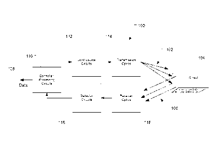
[0017] FIG. 1 is a block diagram of an optical sensor system according to
embodiments
described herein.
[0018] FIG. 2 is a block diagram of optical sensor system light source
circuits according
to embodiments described herein.
[0019] FIG. 3 is a block diagram of optical sensor system light source
circuits including a
plurality of series connected LEDs according to embodiments described herein.
[0020] FIG. 3A is a timing diagram illustrating exemplary timing for
closing switches 51
and S2 according to embodiments described herein.
[0021] FIG. 4 is a circuit diagram of a high voltage supply according to
embodiments
described herein.
[0022] FIG. 5 is a circuit diagram of a switch 51 according to embodiments
described
herein.
DETAILED DESCRIPTION
[0023] FIG. 1 is a simplified block diagram of an optical sensor system 100
according to
embodiments disclosed herein. In general, the optical sensor system 100 emits
light 102, e.g.
infrared (IR) light, that is reflected by an object 104, and receives the
reflected light 106 to
identify the distance to the object 104 and/or to map an image of the object
104. In some
embodiments, for example, the system may be implemented as a collision
avoidance sensor,
e.g. a back-up sensor, for an automotive vehicle. In a back-up sensor
application, for
example, the system provides a data output 108 indicating distance from the
rear of the
vehicle to an object 104 for assisting a driver of the vehicle in avoiding
inadvertent contact
with the object 104 when moving in reverse. Although systems and methods
consistent with
the present disclosure may be described in connection with a particular
application, those of
ordinary skill in the art will recognize that a wide variety of applications
are possible. For
example, systems and methods consistent with the present disclosure may be
implemented in
Page 5 of 17
CA 02755013 2011-09-15
WO 2010/117502 PCT/US2010/024757
optical sensors for range finding applications, or any application involving
identification
and/or imaging of a target object.
[0024] Those of ordinary skilled in the art will recognize that the optical
sensor system
100 has been depicted in highly simplified form for ease of explanation. The
optical sensor
system 100 shown in FIG. 1 includes controller/processing circuits 110, light
source circuits
112, transmission optics 114, receiver optics 116 and detector circuits 118.
The
controller/processing circuits 110 may be known circuits for controlling
modulation of a light
source of the light source circuits and for processing received data to
generate an output data
stream representative of the distance from the sensor to the object and/or an
electronic image
of the object. Controller/processing circuits 110 may, for example, be any of
the depth sensor
controller/processing circuits commercially available from Canesta, Inc. of
Sunnyvale, CA.
[0025] The light source circuits 112 may include known circuitry for
driving the light
source in response to control outputs from the controller/processing circuits
110, and may
include circuitry consistent with the present disclosure. The transmission
optics 114 may
include known optical components for directing light output from the light
source to provide
a system field of view encompassing the object(s) of interest. The receiver
optics 116 may
include known optical components for receiving light reflected from the object
of interest and
directing the received light to the detector circuits 118. The detector
circuits 118 may include
known light detectors, e.g. arranged in an array of pixels, for converting the
received light
into electrical signals provided to the control/processing circuits 110. The
detector circuits
118 may, for example, be any of the detector circuits commercially available
from Canesta,
Inc. of Sunnyvale, CA. The control processing circuits 110 may calculate
distance to various
points on the object and within the system field of view, e.g. using phase
shift in the received
light to calculate time of flight and distance, to provide the data output
indicating distance to
the object and/or mapping the object to provide a three-dimensional image
thereof.
[0026] FIG. 2 is a simplified block diagram of the light source circuits
112 according to
embodiments described herein. The light source circuits 112 include a power
supply 202, a
current source 204 coupled to the output of the power supply 202, a plurality
of series
connected plurality of series connected LEDs 206 coupled to the current source
204, a high
voltage supply circuit 208 coupled to the current source 204, and driver
circuits 210 for
controlling switches 51 and S2 to turn the plurality of series connected LEDs
206 off and on
at a predetermined frequency, i.e. modulate the plurality of series connected
LEDs 206.
Connecting the plurality of series connected LEDs 206 in series according to
embodiments
described herein avoids phase differences between LED outputs and provides
cost efficiency.
Page 6 of 17
CA 02755013 2011-09-15
WO 2010/117502 PCT/US2010/024757
The term "coupled" as used herein refers to any connection, coupling, link or
the like by
which signals carried by one system element are imparted to the "coupled"
element. Such
"coupled" devices, or signals and devices, are not necessarily directly
connected to one
another and may be separated by intermediate components or devices that may
manipulate or
modify such signals. The driver circuits 210 may take one of any known
configuration or
configuration described herein.
[0027] The power supply 202 may take any known configuration for receiving
an input
voltage from an input voltage source 212 and providing a regulated direct
current (DC)
voltage output. The input voltage source 212 may be, as is shown in FIG. 2, a
DC source,
e.g. a vehicle battery, and the power supply 202 may be, as is shown in FIG.
2, a known DC-
DC converter for converting the DC source voltage to a regulated DC voltage at
the output of
the power supply 202. Known DC-DC converters include, for example, buck
converters,
boost converters, single ended primary inductor converter (SEPIC), etc. In
some
embodiments, a SEPIC converter may be used to allow a regulated DC output
voltage that is
greater than, less than, or equal to the input voltage. SEPIC converter and
SEPIC converter
controller configurations are well-known to those of ordinary skill in the
art. One SEPIC
converter controller useful in connection a system consistent with the present
disclosure is
commercially available from Linear Technology Corporation, as model number
LTC18710.
Though FIG. 2 shows a DC source voltage, those of ordinary skill in the art
will recognize
that an alternating current (AC) input may alternatively be used and the power
supply 202
may then include a known AC-DC converter for providing a regulated DC output
voltage.
[0028] The current source 204 may provide a constant current to the
plurality of series
connected LEDs 206 for energizing the plurality of series connected LEDs 206
when the
switch 51 is closed by the driver circuits 210. The switch 51 is illustrated
in diagrammatic
form for ease of explanation, but may take the form of any of a variety of
configurations
known to those of ordinary skill in the art. For example, the switch 51 may be
a transistor
configuration that conducts current under the control of the driver circuit
output.
[0029] The driver circuits 210 may be configured to open and close the
switch 51 at a
predetermined frequency under the control of control signals 214 from the
controller/processing circuits 110. In some embodiments, for example, the
driver circuits 210
may open and close the switch 51 at a frequency of about 40MHz. The current
source 204
may thus provide a driving current to the plurality of series connected LEDs
206 at the
predetermined frequency for modulating the plurality of series connected LEDs
206, i.e.
turning the the plurality of series connected LEDs 206 on and off
Page 7 of 17
CA 02755013 2011-09-15
WO 2010/117502 PCT/US2010/024757
[0030] The high voltage supply circuit 208 may be coupled to the plurality
of series
connected LEDs 206 through the switch S2. The switch S2 may be closed by the
driver
circuits 210 under the control of control signals from the
controller/processing circuits 110
during the start of the "on" time for the plurality of series connected LEDs
206. A high
voltage, i.e. higher than the output voltage of the power supply 202, may be
coupled from the
power supply 202 to the high voltage supply circuit 208, e.g. by path 218, and
the high
voltage supply circuit 208 may provide a high voltage output Vh across the
plurality of series
connected LEDs 206. In some embodiments, for example, the high voltage output
Vh may be
about 18V, whereas the regulated DC output of the power supply 202 may be
about 10V.
[0031] The high voltage supply circuit 208 may thus increase the voltage
across the
plurality of series connected LEDs 206 to a higher voltage than can be
established by the
current source 204 to overcome the parasitic inductance in the plurality of
series connected
LEDs 206 and decrease the rise time of the current through the plurality of
series connected
LEDs 206. After the start of the "on" time for the plurality of series
connected LEDs 206, the
switch S2 may open to disconnect the high voltage supply circuit 208 from the
plurality of
series connected LEDs 206, and the switch Si may be closed to allow the
current source 204
to drive the plurality of series connected LEDs 206 through the rest of the
"on" time. The
switch S2 is illustrated in diagrammatic form for ease of explanation, but may
take any of a
variety of configurations known to those of ordinary skill in the art. For
example, the switch
S2 may be a transistor configuration that conducts current under the control
of the output of
the driver circuits 210.
[0032] FIG. 3 illustrates a light source circuit including a plurality of
series connected
LEDs 206a, e.g. infrared LEDs, according to embodiments described herein.
Diodes D8, D9,
D10, and Dll are coupled across diodes D3, D4, D5, and D6, respectively, to
take up any
back voltage across the diodes D3, D4, D5, and D6. Although FIG. 3 shows four
series
connected LEDs (that is, D3, D4, D5, and D6), it is to be understood that any
number of
LEDs may be connected in series to provide a plurality of series connected
LEDs.
[0033] In FIG. 3, the current source 204a includes a resistor R1 in series
with an inductor
Li, and a diode D1 coupled in parallel across the series combination of the
resistor R1 and
the inductor Ll. A feedback path 302 to the power supply 202 is provided by a
current
monitor 304 and a diode D2. As shown, the regulated DC output Vs of the power
supply 202
may be coupled to the input of the current source 204a at the resistor Rl. The
driver circuits
210 may open and close the switch Si at a high frequency, e.g. 40MHz. When the
switch Si
is closed, a current Is flows through the series combination of the resistor
R1, the inductor Li,
Page 8 of 17
CA 02755013 2011-09-15
WO 2010/117502 PCT/US2010/024757
and to the plurality of series connected LEDs 206a for energizing the
plurality of series
connected LEDs 206a. The inductor Li thus establishes a constant current
source and limits
the current L through the plurality of series connected LEDs 206a when the
switch Si is
closed. When the switch Si is open, however, no current flows through the
plurality of series
connected LEDs 206a, and the current IL through the inductor Li is diverted
through the
diode D1 to maintain current through the inductor Ll.
[0034] As shown, the current monitor 304 may be coupled across the resistor
R1 for
sensing the voltage drop across the resistor Rl. The current monitor 304 may
take any
configuration known to those of ordinary skill in the art. In some
embodiments, for example,
the current monitor 304 may be configured using a current shunt monitor
available from
Texas Instruments under model number INA138. The current monitor 304 may
provide a
feedback output to the power supply 202, e.g. through the diode D2.
[0035] In response to the feedback from the current monitor 304 and during
the time
when the switch Si is closed, the power supply 202 may be configured to adjust
the supply
voltage Vs to a voltage that will allow the inductor Li to recharge. In some
embodiments, the
feedback path 302 maybe coupled to a voltage feedback path of the power supply
202 to
provide a constant current control loop that takes control away from the
voltage control loop
during the time when the switch Si is closed, i.e. "on" time for the plurality
of series
connected LEDs 206a. A variety of configurations for providing an adjustable
supply voltage
in response to the current monitor feedback are well-known to those of
ordinary skill in the
art. In one embodiment, for example, the power supply 202 may be configured as
a known
converter, e.g. a SEPIC converter, and a known converter controller, e.g. a
SEPIC controller
configured to control the converter output in response to the current monitor
feedback. A
constant current may thus be established through the inductor Li when the
switch Si is
closed, i.e. when the diodes D3, D4, D5, and D6 are "on" and emitting light.
[0036] In FIG. 3, the high voltage supply circuit 208 is coupled to the
plurality of series
connected LEDs 206a through the switch S2. The switch S2 may be closed by the
driver
circuits 210 under the control of control signals from the
controller/processing circuits 118
during the start of the "on" time for the plurality of series connected LEDs
206a. When the
voltage output of the high voltage supply circuit 208 is coupled to the
plurality of series
connected LEDs 206a, i.e. the switch S2 is closed, a diode D7 blocks the high
voltage output
of the high voltage supply circuit 208 from the current source 204a. After the
start of the
"on" time for the plurality of series connected LEDs 206a, the switch S2 may
open to
disconnect the high voltage supply circuit 208 from the plurality of series
connected LEDs
Page 9 of 17
CA 02755013 2011-09-15
WO 2010/117502
PCT/US2010/024757
206a. The diode D7 may then conduct and the current source 204a may drive the
plurality of
series connected LEDs 206a through the rest of the "on" time.
[0037] FIG. 3A is in exemplary timing diagram illustrating the timing of
the signal from
the driving circuits for closing the switches Si and S2. As shown, the switch
S2 may be
closed at the start ts of the "on" time for a plurality of series connected
LEDs to initially
provide a high voltage across the plurality of series connected LEDs to
overcome any
parasitic inductance in the LEDs and thereby decrease the rise time of the
current through the
plurality of series connected LEDs. The switch Si may then close, but the high
voltage
output Vh of the high voltage supply may prevent the current source from
sourcing current to
the plurality of series connected LEDs while the switch S2 is still closed.
The switch S2 may
then open allowing the diode D7 to conduct and the current source to drive the
plurality of
series connected LEDs during the remainder of the "on" time.
[0038] In FIG. 3A, driving current for the plurality of series connected
LEDs is initially
provided by the high voltage supply, e.g. by closing the switch S2 as
described above. The
plurality of series connected LEDs may exhibit significant parasitic
inductance that limits a
rise time of the current source current therethrough. The high voltage output
of the high
voltage supply overcomes the parasitic inductance of the plurality of series
connected LEDs
to allow a faster rise time of the current through the plurality of series
connected LEDs than
could be achieved by current from the current source. When the switch S2 opens
and the
switch Si is closed, the diode D7 may conduct to allow the current source to
drive the
plurality of series connected LEDs in the remainder of "on" time of the
plurality of series
connected LEDs. This configuration allows a relatively fast rise time of the
current through
the plurality of series connected LEDs and a constant current from the current
source through
the plurality of series connected LEDs to allow switching/modulation of the
output of the
plurality of series connected LEDs at relatively high frequency, e.g. 40MHz.
It is to be
understood, however, that in some embodiments the high voltage supply is
optional and may
be omitted when the faster rise time provided thereby is not desired or
necessary.
[0039] Those of ordinary skill in the art will recognize that a high
voltage supply may be
provided in a variety of configurations. FIG. 4 is a circuit diagram of a high
voltage supply
circuit 208a and a switch 52a. In FIG. 4, the switch 52a is implemented using
a first metal-
oxide semiconductor field-effect transistor (MOSFET) Q1 and a second metal-
oxide
semiconductor field-effect transistor (MOSFET) Q2 configured and biased in
cascode
configuration. The first MOSFET Q1 is in a common source configuration and the
second
MOSFET Q2 is in a common gate configuration.
Page 10 of 17
CA 02755013 2011-09-15
WO 2010/117502 PCT/US2010/024757
[0040] A high voltage input is coupled to the source of the first MOSFET Q1
from a node
in the power supply that has a higher voltage than the output voltage of the
power supply. In
some embodiments, for example, the drain of the power MOSFET in a SEPIC
converter
implementing a model number LTC18710 SEPIC converter controller available from
Linear
Technology Corporation may be coupled to the source of the first MOSFET Ql.
The gate of
the first MOSFET Q1 may be coupled to the drive circuit. The drive circuit may
provide a
square wave signal to the gate of the first MOSFET Q1 for causing the first
MOSFET Q1 and
the second MOSFET Q2 to conduct periodically, i.e. to open and close the
switch S2a as
described above. When the first MOSFET Q1 and the second MOSFET Q2 conduct,
the high
voltage across a resistor R2 and a capacitor Cl is provided across the
plurality of series
connected LEDs.
[0041] As discussed above the switch Si may be provided in a variety of
configurations
known to those of ordinary skill in the art. FIG. 5 is a circuit diagram of a
switch Si a. In
FIG. 5, the switch Sla is implemented using a first metal-oxide semiconductor
field-effect
transistor (MOSFET) Q1 and a second metal-oxide semiconductor field-effect
transistor
(MOSFET) Q2 configured and biased in cascode configuration. The first MOSFET
Q1 is in
a common source configuration and the second MOSFET Q2 is in a common gate
configuration and driven by the first MOSFET Ql. This configuration allows a
low
impedance on the drain of the first MOSFET Ql, thereby reducing the effects of
Miller
capacitance. Also, the voltage at the drain of the first MOSFET Q1 is no
greater than the gate
voltage of the second MOSFET Q2. Accordingly, the switching speed of the first
MOSFET
Q1 is independent of the voltage on the drain of the second MOSFET Q2. In some
embodiments, two switches configured as illustrated in FIG. 5 may be used in
parallel.
[0042] Unless otherwise stated, use of the word "substantially" may be
construed to
include a precise relationship, condition, arrangement, orientation, and/or
other characteristic,
and deviations thereof as understood by one of ordinary skill in the art, to
the extent that such
deviations do not materially affect the disclosed methods and systems.
[0043] Throughout the entirety of the present disclosure, use of the
articles "a" or "an" to
modify a noun may be understood to be used for convenience and to include one,
or more
than one, of the modified noun, unless otherwise specifically stated.
[0044] Elements, components, modules, and/or parts thereof that are
described and/or
otherwise portrayed through the figures to communicate with, be associated
with, and/or be
based on, something else, may be understood to so communicate, be associated
with, and or
be based on in a direct and/or indirect manner, unless otherwise stipulated
herein.
Page 11 of 17
CA 02755013 2011-09-15
WO 2010/117502
PCT/US2010/024757
[0045] Although the methods and systems have been described relative to a
specific
embodiment thereof, they are not so limited. Obviously many modifications and
variations
may become apparent in light of the above teachings. Many additional changes
in the details,
materials, and arrangement of parts, herein described and illustrated, may be
made by those
skilled in the art.
Page 12 of 17