Note: Descriptions are shown in the official language in which they were submitted.
CA 2757033 2017-03-30
81669049
1
System and Method for demodulating a signal
FIELD OF THE INVENTION
The present invention relates in general to a system and method for
demodulating a phase-modulated or frequency-modulated signal.
BACKGROUND OF THE INVENTION
Figure 1 schematically illustrates an optical computer mouse I known from
prior art, comprising a laser device 2. The laser device is implemented as a
semiconductor
laser, as known per se. The mouse is moved over a surface 4, for instance a
desktop. From a
power source not shown for sake of simplicity, the laser device 2 receives an
electric current,
and as a result the laser 2 emits a laser beam 3 with a certain wavelength,
which is reflected
by the surface 4. Part of the laser light is reflected back towards the laser.
It is possible to
derive, from this reflected laser light, a signal representing velocity of the
movement of the
mouse 1 with respect to the surface.
Figure 2 is a schematic diagram illustrating the measuring principle known
from prior art. The laser 2 comprises a semi-transparent front mirror 11 and a
semi-
transparent rear mirror 12, with a laser medium 13 (semiconductor body)
between said two
mirrors. It is noted that the mirrors 11, 12 are shown as two-dimensional
structures, but in
practice the mirrors 11, 12 will have a layered structure.
The laser light within the laser medium 13 is indicated as main laser light
LO.
Part of the laser light passes the front mirror 11 and forms the output beam
3; this light is also
indicated Ll. Likewise, part of the laser light passes the rear mirror 12 and
forms a measuring
beam 5; this light is also indicated L2.
The object 4 can be considered to constitute an external mirror with diffuse
properties, and reflects the incoming beam Li: this is indicated as a
reflected beam L3. In
CA 2757033 2017-03-30
81669049
1 a
the drawing, the reflected beam L3 is shown as being a one-dimensional beam
making an
angle with the incoming beam Li, but in practice the reflected beam L3 will
have a certain
spatial distribution and a portion of this reflected beam L3 will be directed
towards the front
mirror 11. Thus, the object 4 can be considered as defining an external cavity
together with
the front mirror 11.
CA 2757033 2017-03-30
81669049
2
Under stationary conditions, the light LO within the laser medium 13 forms a
standing wave.
Likewise, light Li and L3 in the external cavity forms a standing wave which,
through the
front mirror 11, interferes with the light LO within the laser medium 13. The
measuring beam
has a constant intensity.
5 Assume that the object 4 is moving away from the laser 2. This
means that the
length of the interference cavity between the front mirror 11 and the object 4
is increasing, i.e.
the number of standing waves fitting between the front minor 11 and the object
4 is
increasing. Consequently, the interference state at the location of the front
mirror 11 changes
from fully constructive to fully destructive and back. This has influence on
the interference
state in the laser medium 13, which in turn has influence on the intensity of
light L5 of the
measuring beam 5. As a result, this light L5 has intensity fluctuations at a
frequency fD that is
proportional to the velocity of movement of the object 4 with respect to the
laser 2, i.e. the
component thereof along the optical axis. It should be clear that the
measuring beam 5 can be
detected by an optical sensor, and that its output signal can be processed by
a signal processor
in order to process these intensity fluctuations and to calculate the object
velocity therefrom. It
is noted that said frequency fD is equal to the Doppler frequency.
It has already been proposed in prior art to solve this problem by supplying
the
laser with a triangularly modulated laser current, as illustrated in figures
3A-3D. The laser
current is varied in a linear manner between two extreme values 11 and 12
having the same
sign. During one half of a current period, the laser current I is increasing
from II to 12, the
change rate R1 = dl/dt being substantially constant. During another half of a
current period,
the laser current I is decreasing from 12 to Ii, the change rate R2 = dI/dt
being substantially
constant; typically. R2 = -R1. Increasing/decreasing the laser current causes
an
increase/decrease of the laser temperature (as illustrated in figure 3B),
which in turn causes an
increase/decrease of the wavelength of the laser light (as illustrated in
figure 3C) with a
substantially constant change rate dk/dt, in which X, indicates the laser
wavelength. The result
can be explained as follows. Assume that the object is moving away from the
laser, so that the
length of the interference cavity between the front mirror 11 and the object 4
is increasing. If
the current magnitude and hence the laser wavelength is also increasing, the
frequency of the
CA 2757033 2017-03-30
=
81669049
2a
intensity fluctuations of measuring light L5 is reduced; this is illustrated
by a peak fl in the
frequency spectrum of figure 3D. The reduced frequency may even become equal
to zero if
D/k remains constant, in which D indicates the distance between the front
mirror 11 and the
object 4. Conversely, if the laser wavelength is decreasing, the frequency of
the intensity
fluctuations of measuring light L5 is increased; this is illustrated by a peak
f2 in the frequency
spectrum
:A 0275'033 201 -Crd-27
64869-1718
3
of figure 36. It is noted that the shift IfD f1I is equal to the shift IfD
f2I. The spectrum
of the intensity fluctuations of measuring light L5 thus shows two peaks f1
and f2, as
schematically illustrated in figure 3B. If on the other hand the object is
moving
towards the laser, a frequency spectrum with two frequency peaks is again
obtained,
but now the lower frequency is obtained during the periods that the current
magnitude
is decreasing. Thus, the direction of movement can be determined by
determining
whether the frequency is higher during the periods that the current magnitude
is
decreasing or during the periods that the current magnitude is increasing. It
should
be clear that this information can be derived from the measuring signal
relatively
easily by a suitably programmed signal processor.
For a more detailed explanation, reference is made to US patent
7.339.683.
A problem in this respect is that the frequency needs to be determined
during the periods that the current is increasing and during the periods that
the
current is decreasing, resulting in 2 discrete frequencies. Thus, measurements
for
measuring a first frequency always start at the beginnings of the periods that
the
current is increasing and they always end at the ends of these periods, while
measurements for measuring a second frequency always start at the beginnings
of
the periods that the current is decreasing and they always end at the ends of
these
periods. Thus, these measurements are interrupted regularly, leading to
interruptions
in the data acquisition and a general loss of information. For a high accuracy
sensor,
however, it is desired to be able to (nearly) continuously track a
displacement signal
without these interruptions. For instance by tracking the phase of the
displacement
signal. Thus a method is needed that allows continuous tracking of a
displacement
signal while also providing direction detection.
Stated more generally, a signal may contain multiple signal
components, and the present invention aims to provide a signal processor
capable of
recognizing the exact frequency of a certain signal component in the received
signal.
:A 0275'033 201 -Crd-27
64869-1718
4
Normally, a PLL (Phase Locked Loop) is used in a situation where the frequency
of
the frequency component is already known in approximation. For allowing the
PLL to
lock in on this frequency, it is known to start with the PLL having a
relatively large
bandwidth and then reducing the bandwidth while keeping the signal component
within the band. However, there are cases where the received signal actually
comprises multiple frequency components, of which the frequency distance may
be
relatively small, and of which the exact frequency is not approximately known
in
advance; the situation described in the introduction is an example of such
case. If
the conventional method of a PLL with an initially large bandwidth is used,
chances
are that the PLL will lock in on an incorrect frequency.
It is a particular object of some embodiments of the present invention to
provide a device capable of reliably demodulating the received signal of such
situation.
SUMMARY OF THE INVENTION
According to one aspect of the present invention, a demodulating
system for demodulating a phase-modulated signal comprises:
1) a digital demodulator comprising a digital FLL (Frequency
Locked
Loop), which contains a controllable reference frequency generator, the
digital
demodulator being capable of performing complex demodulation; and
2) a digital FFT device capable of performing a complex Fast Fourier
Transformation (FFT);
3) a memory containing information defining an expected frequency
characteristic of the phase-modulated signal;
4) an analyzing device.
The said information reflects the fact that the received phase-modulated
signal is generated by a known process, and that the known process results in
:A 0275'033 201 -Crd-27
64869-1718
signals having a frequency characteristic that can be described by a
predetermined
formula. In the case of an optical displacement sensor as described above, the
frequency characteristic can be described by a Bessel series.
The input signal of the demodulating system is subjected to complex
5 demodulation by the digital demodulator. The demodulator output signal
has a
frequency spectrum that contains a primary peak and at least one but typically
a
plurality of secondary peaks. The primary peak has a frequency corresponding
to the
frequency which the demodulator has recognized as being the main signal
component(s). It may however be that the demodulator has locked in on the
wrong
frequency, which means that the reference frequency generator is set to a
wrong
frequency.
The digital FFT device receives the said information from said memory,
and thus, on the basis of the frequency characteristic to be expected, the
digital FFT
device performs complex Fast Fourier Transformation (FFT) on the demodulator
.. output signal.
The output signal of the FFT device is provided to the analyzing device.
The information contained in the output signal of the FFT device allows the
analyzing
device to determine whether or not the primary peak in the input signal of the
FFT
device is a correct peak in accordance with the expected frequency
characteristic. If
it is found that the primary peak is not correct, the information contained in
the output
signal of the FFT device also allows the analyzing device to determine the
difference
Af between the current frequency of the said primary peak and the correct
frequency.
Based on this information, the analyzing device provides an error signal to
the digital
demodulator, which in response adapts the frequency of its reference frequency
.. generator by the said difference Af such as to be adjusted to the correct
frequency.
Thus, very quickly, the digital demodulator locks in on the correct
frequency. Now its output signal is also provided to a second analyzing
device. The
CA 2757033 2017-03-30
81669049
5a
information contained in the output signal of the demodulator allows the
second analyzing
device to calculate velocity and direction of movement.
According to another aspect of the present invention, there is provided a
demodulating system for demodulating a phase-modulated input signal (Si), the
phase-
modulated input signal comprising a carrier signal to which a phase modulation
has been
applied, the demodulating system comprising: a complex demodulator, having a
first input
for receiving the phase-modulated input signal (Si) and being configured to
perform complex
multiplication of the phase-modulated input signal (Si) with an approximation
of an inverse of
the phase modulation and in response thereto to output a demodulated product
signal; and a
spectrum analyzing device receiving the demodulated product signal produced by
the complex
demodulator and capable of analyzing the frequency spectrum of the demodulated
product
signal.
According to another aspect of the present invention, there is provided a
motion detector capable of detecting motion direction of an object moving with
respect to the
detector, the detector comprising: a laser comprising a semi-transparent front
mirror, a semi-
transparent rear mirror, and a semiconductor laser body between said two
mirrors, the laser
being designed to output an output laser beam with laser output light (Li) at
its front mirror
and to output a measuring beam with measuring light (L2) at its rear mirror,
the laser further
being designed to allow at least a portion of reflected light (L3) to
interfere with main light
(LO) within the laser body; a controllable laser current source for supplying
the laser with
laser current (I) such as to generate the main laser light (LO) within the
laser body; a controller
for controlling the laser current source; a light detector for detecting at
least a portion of the
measuring light (L2) and for supplying a measuring signal (Sm) to the
controller; wherein the
controller is designed to control the laser current source such that it
modulates the laser
current (I) in order to modulate the wavelength of the laser output light
(L1); and wherein the
controller is designed to analyze the frequency spectrum of the detected light
(L2) in
conjunction with the modulated laser current (I) in order to determine the
speed and direction
of movement of the object; wherein the controller comprises a demodulating
system as
described herein.
CA 2757033 2017-03-30
81669049
5b
According to yet another aspect of the present invention, there is provided a
method of demodulating a phase-modulated input signal (Si), the phase-
modulated input
signal comprising a carrier signal to which a phase modulation has been
applied, the method
comprising the steps of: performing complex multiplication of the phase-
modulated input
signal (Si) signal with an approximation of an inverse of the phase
modulation; outputting in
response to the complex multiplication a demodulated product signal; analyzing
the frequency
spectrum of the demodulated product signal produced by the complex
multiplication of the
phase-modulated input signal (Si).
Further advantageous elaborations are mentioned in the dependent claims.
BRIEF DESCRIPTION OF THE DRAWINGS
These and other aspects, features and advantages of the present invention will
be further explained by the following description of one or more preferred
embodiments with
reference to the drawings, in which same reference numerals indicate same or
similar parts,
and in which:
Figure 1 schematically shows an optical computer mouse with a laser detector
for detecting movement of the mouse with respect to a surface;
Figure 2 is a diagram schematically illustrating the measuring principle
underlying the laser movement detector;
Figure 3A schematically illustrates a triangularly modulated laser current;
Figure 3B schematically illustrates the laser temperature caused by the
modulated laser current;
Figure 3C schematically illustrates the laser wavelength resulting from the
modulated laser temperature;
Figure 3D schematically illustrates the frequency spectrum of the laser
detector
output signal in the case of a movement;
CA 2757033 2017-03-30
81669049
5c
Figures 4 and 5 are graphs illustrating phase modulation;
Figures 6-7 are graphs illustrating frequency spectra of a phase-modulated
signal;
:A 0275'033 201' -Crd-27
WO 2010/113074 PCT/1B2010/051267
6
Figure 8 is a block diagram illustrating a demodulating system according to
the present invention;
Figures 9-14 are graphs illustrating frequency spectra after demodulation
according to the present invention.
DETAILED DESCRIPTION OF THE INVENTION
In the following, an explanation will be given of demodulation of a phase
modulated carrier to determine carrier frequency and carrier frequency sign.
It will be shown
that the signal frequency of a signal with a signal frequency and an
approximately known
phase modulation can be determined, including the sign of the frequency and
with frequency
values arbitrarily close to zero. This is accomplished by a complex
demodulation of the
signals with a phase that is opposite to the signal phase modulation. The
Demodulation
function or amplitude may be chosen specifically for certain signal frequency
ranges. While
there is tolerance to mismatch between modulation and demodulation phase
functions, this
mismatch should be limited such that in general the modulation function or
amplitude may
also be adapted for different signal frequency ranges. Signal frequency can be
determined
after the demodulation, for instance with a frequency locked loop (FLL) and/or
with a CFFT.
A CFFT is particularly useful to determine approximate signal frequency to
support the
locking process of an FLL and to determine if the modulation and demodulation
phase
amplitudes are matched.
Phase modulated signal
Assume a phase-modulated signal, consisting of a carrier signal having a
carrier frequency o) of which the phase is modulated according to
p(t)=P*cos(com*t)
where P is the modulation amplitude in radians, and ct)rn is the modulation
frequency.
Figure 4 is a graph showing an example of such a phase modulation for large
phase modulation, with P = it and fm = cona/27r = 1 MHz.
The resulting phase-modulated signal can be described by the formula:
f(t)=cos(o)*t+p(t))
An example of this signal is shown in figure 5, with a carrier frequency
f = o)/27r = 300 kHz.
As is known from communication theory, such phase-modulated signal has a
spectrum that is determined by a series of Bessel functions, and for the
example given above
:A 0275'033 201' -Crd-27
WO 2010/113074 PCT/1B2010/051267
7
the spectrum is shown in figure 6 as found from a complex Fourier
transformation. The
complex FFT spectrum is shown in the left-hand graph of figure 6, while the
right-hand
graph of figure 6 shows the FFT spectrum. Note that the complex FFT spectrum
contains
positive and negative frequencies; in the real domain, only positive
frequencies can be
measured, resulting in the spectrum shown to the right.
The height of the different peaks in the spectrum is determined by the phase
modulation depth P. Figure 7 shows the FFT spectrum for an example with
P=0.5*n and
co = 300 kHz (left) and co = -300 kHz (right), respectively. It can be seen
that these spectra
yield no information about the sign of the frequency, which corresponds to the
direction of
movement of an object in the example discussed in the introduction. It is
noted that this can
also be recognized in the CFFT spectrum of figure 6, in that this spectrum is
symmetrical
with respect to zero. Furthermore, it can be seen that the strongest peaks may
occur at
frequencies different from the Doppler frequency of 300 kHz, recognizable as
one of the
smaller peaks.
The present invention aims to provide a demodulating system that is capable
of receiving phase-modulated signals of the type as described above, having
frequency
spectra similar to the spectra as described above, and that is capable of
performing such
operation as to provide an output signal, also indicated as demodulated
signal, of which the
frequency spectrum has a clear signal at the carrier frequency and clearly
distinguishes
between positive and negative modulation frequency. A block diagram of such
demodulating
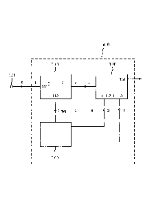
system 100 proposed by the present invention is shown in figure 8. The
demodulating system
100 has an input 101 receiving the phase-modulated input signal Si.
Phase demodulation
The demodulating system 100 comprises a complex demodulator 110, having
a first input 111 and a second input 112. At its first input 111, the complex
demodulator 110
receives the phase-modulated input signal Si. At its second input 112, the
complex
demodulator 110 receives a signal Spmf that contains information on the phase
modulation of
the input signal Si. The complex demodulator 110 is designed to use this
information to
perform a complex multiplication of the input signal Si with an approximation
of the inverse
of the phase modulation, according to the following formula:
g(t)=f(t)*exp(-i*p(t)*u)
where u is a factor equal to 1 or almost equal to 1.
For the example of f(t) given above, this results in:
:A 0275'033 201' -Crd-27
WO 2010/113074 PCT/1B2010/051267
8
g(t)=0.5*}exp[i*(co*t + p(t))]+ exp[-i*(a)*t + p(0)]}* exp(-i*p(t)*u)
or
g(t)=0.5*}expri*(co*t + p(t)*(1-u))]+ expr-i*(o.)*t + p(t)*(1+u))]}
Figure 9 shows the resulting spectra of g(t), for three different values of P,
for
an example where the carrier frequency is 300 kHz and u = 0.75 (indicating 25%
error in the
estimate of u). The modulation frequency fm is 1 MHz. The sampling frequency
is 16 MHz,
so that the Fourier transformation provides output in the -8 to 8 MHz range,
but the figure
only shows the -4 to 4 MHz range.
It can clearly be seen that the strongest peak corresponds to the positive
carrier
frequency of 300 kHz; the vertical dotted lines indicate the peaks of the
Bessel series
frequencies belonging to this strongest peak. A vertical arrow indicates the
frequency peak
having the negative carrier frequency of -300 kHz; this frequency will be
indicated as the
opposite carrier frequency. The remaining (non-marked) peaks are the Bessel
series
frequencies around this opposite carrier frequency.
All the spectra are the result of complex Fourier transforms, as the input
signal
is a complex signal. The highest peak in the spectra corresponds to the
Doppler frequency
(carrier frequency of the phase-modulated input signal). There are side-peaks
created by the
residual phase modulation (1-u)*p(t), the relative level of these side-peaks
to the main peak is
determined by (1-u)*P. When u=1, the sidebands are absent. The sign of (1-u)*P
determines
the phase of the side-peaks. The spectrum can thus be used to determine and to
control u
and/or P. Opposite to the highest peak there is a second peak at the opposite
(negative)
frequency; this peak is weaker and has more side-peaks, due to the deeper
phase modulation
of this peak with phase amplitude (l+u)*P. By increasing P, the second peak
can get
completely suppressed and the spectrum is scattered over a wider range.
Figure 10 shows the resulting spectra of g(t), for the same example but with
u=1 (perfect demodulation) and P=7E. The Doppler peak is strongest and does
not cause any
sidebands. The opposite Doppler peak is more than 10 dB weaker and has many
sidebands
scattered over a large frequency range. The spectrum around the opposite
Doppler peak can
thus also be used to determine the phase modulation depth.
Demodulation of low frequency signals
A special case occurs when the carrier frequency is near zero. In this case
the
carrier frequency and opposite carrier frequency practically overlap and so do
their
:A 0275'033 201 -Crd-27
WO 2010/113074
PCT/1B2010/051267
9
sidebands. However, the wide spectrum of the opposite frequency still allows
an estimation
of the modulation depth. Figure 11 is a graph comparable to figure 10, for an
example where
the carrier frequency (Doppler frequency) is 50 kHz. For the same situation,
figure 11 shows
a zoomed-in version of this spectrum, for the range -1 to +1 MHz. While a CFFT
with low
resolution can only determine that the carrier frequency (i.e. speed) is low,
a CFFT with
sufficient resolution can still determine the sign of the frequency (i.e.
direction of motion).
It has thus been shown that demodulation of a phase modulated signal by
using a complex rotation with the inverse of the modulation phase, or an
approximation
thereof, allows both signal frequency and frequency sign to be determined. In
the case of a
laser self-mixing sensor, this frequency will be the Doppler frequency. The
phase modulation
is allowed to be large, so large that the signal frequency cannot be
determined anymore by
looking at the signal spectrum prior to the complex demodulation. It is well
known that the
frequency sign cannot be determined from the spectrum of a real signal, but
with the complex
demodulation the resulting spectrum does allow determination of the frequency
sign.
Thus, the demodulation device 100 comprises a spectrum analyzing device
130, receiving the output signal from the complex demodulator 110, and
providing as output,
at a first output 131, the main frequency of the demodulated signal
(corresponding to the
carrier frequency of the input signal Si) and the frequency sign. This
spectrum analyzing
device 130 may be implemented as a CFFT (Complex Fast Fourier Transform)
device, but
this is not the only tool applicable. A PLL or FLL is another option that may
be used as an
alternative or in parallel with a CFFT. A PLL or FLL has at the input a mixer
(complex
rotation) that multiplies the signal with the expected signal frequency
(Doppler frequency in
case of a self-mixing sensor). It is straightforward to include a
multiplication with the
opposite of that frequency at this stage. Both results can then be low pass
filtered to remove
.. frequencies far off the expected frequency (for instance +1- 10 kHz in the
figure above). The
amplitudes of both signals can then be compared and since it is known that the
main signal is
much stronger than the unwanted inverse signal any lock to the weak unwanted
signal can be
detected immediately and prevented.
When the filter bandwidth is large enough to pass both peaks (that is when the
expected Doppler frequency is under the filter bandwidth) then both peaks will
be detected at
each output (that is at the output with the positive Doppler demodulation
frequency and at the
output with the negative Doppler demodulation frequency). For a range of
Doppler
frequencies the amplitude difference between the filter outputs will still be
sufficient to
determine which sign is correct. For lower Doppler frequencies the outputs are
:A 0275'033 201 -Crd-27
WO 2010/113074 PCT/1B2010/051267
indistinguishable and one of the outputs may be chosen, for instance the
output with positive
Doppler frequency demodulation. The phase of the complex signal at that output
can then be
tracked. This phase is added to the phase of the Doppler frequency
demodulation to result in
the total signal phase of the input signal. An error in choosing positive or
negative Doppler
5 frequency for demodulation output will be self-cancelled by this method
so that for all signal
frequencies from negative to positive the PLL or FLL can track phase
accurately.
When the signal (Doppler frequency) is very high, the FLL could also
erroneously lock to a side-peak. To prevent this, the use of a CFFT in
parallel with the FLL is
useful to determine the correct signal frequency and support the FLL to lock
to the correct
10 .. peak. In burst operation the CFFT is particularly useful to push the FLL
demodulation
frequency to the correct value when a good estimate of this demodulation
frequency is not
known prior to the burst.
The complex demodulation is tolerant to errors in the demodulation phase
amplitude, but best results are obtained if the demodulation phase amplitude
is close to the
phase amplitude of the modulated signal. Therefore, the spectrum analyzing
device 130 has a
second output 132 providing an error signal Se that represents an estimate of
the difference
between actual phase amplitude of the modulated signal and demodulation phase
amplitude.
The error in the demodulation phase amplitude can be estimated from sideband
phase and
amplitude of the spectrum around the main frequency or from sideband phase and
amplitude
of a spectrum around an unwanted negative image of the main frequency. The
amplitude of
the unwanted inverted frequency peak relative to the main frequency peak may
also be used
to derive demodulation information. A modulation controller 140 receives the
error signal Se
and uses this signal to generate the phase modulation information signal Spmi
for the complex
demodulator 110.
It should be noted that, while the demodulation phase amplitude should more
or less match the modulation phase amplitude, it is not necessary that this is
achieved by
controlling the demodulation phase amplitude. As an alternative, the
modulation phase
amplitude may be controlled. In a practical implementation, a sensor module
may include the
transmitting laser as well as the receiving sensor, and thus such module
integrates both laser
drive and signal analysis functions. Through the laser drive, the modulation
phase amplitude
can be controlled, in most cases by controlling the amplitude of an AC current
superimposed
on the laser bias current.
Thus, there will generally be a control loop such as:
Spectrum analysis => demodulation amplitude => spectrum => spectrum analysis
:A 0275'033 201' -Crd-27
WO 2010/113074 PCT/1B2010/051267
11
Spectrum analysis => modulation amplitude => spectrum => spectrum analysis
Avoiding lock to unwanted signal components
For an application in a self-mixing sensor, it should be noted that in
reality,
when a self-mixing laser sensor is phase modulated, there usually also is an
amplitude
modulated component in the laser light. This signal occurs at the phase
modulation
frequency. Figure 13 shows the corresponding frequency spectrum for the
example given
(300 kHz signal frequency, 1 MHz modulation frequency, 7c/2 phase modulation
and
demodulation).
The spectrum shows strong unwanted peaks at 0 and at integer multiples of the
modulation frequency of 1 MHz. The FLL could be affected detrimentally by the
proximity
of an unwanted peak due to the signal modulation. This can be mitigated by
shifting the
phase modulation frequency (and thus its spectrum) in dependence of the
Doppler frequency
such that the Doppler frequency is not close to an unwanted peak. When the
sign of the signal
frequency is known (such as for a sensor with an object moving at high speed)
the
modulation could also be turned off all together.
Thus, the spectrum analyzing device 130 may be designed to use the signal
frequency to determine what phase modulation frequency is desirable to obtain
a spectrum
that is easy to analyze with a CFFT and to lock to for an FLL. The CFFT can
also be used to
determine the signal frequency range such that a suitable modulation frequency
can be
chosen. At a third output 133, the spectrum analyzing device 130 provides a
signal Sf
representing the desired phase modulation frequency, and this is also received
by the
modulation controller 140 and used to generate the phase modulation
information signal Spmi
for the complex demodulator 110. Thus, the phase modulation information signal
Spmi may
contain information for setting the phase modulation frequency and/or the
phase modulation
amplitude.
For very low speed, a residual amplitude modulation leads to a peak close to 0
Hz. This peak can be suppressed by choosing appropriate demodulation phase
amplitude. For
the example given (with u=1) with residual AM modulation for instance at 1.22z
demodulation phase amplitude, the peak due to residual AM modulation can be
extinguished.
The proper phase demodulation amplitude for cancellation of residual AM
modulation
depends on system design. Furthermore, other measures are possible such as
cancellation of
residual AM modulation before the signal is demodulated. A combination of such
measures
can be used to remove the effect of residual AM modulation at low frequencies.
:A 0275'033 201 -Crd-27
WO 2010/113074 PCT/1B2010/051267
12
Figure 14 is an example of a case where the demodulation phase amplitude
and function would be chosen specifically to obtain good suppression of
unwanted AM
modulation in the input signal. Since the phase modulation and demodulation
functions
should match, this is an example of a case where the phase modulation would be
controlled
to obtain this match rather than the phase demodulation. It is also an example
of a case where
for low signal frequency (or low Doppler frequency in a self-mixing sensor) a
particular
phase modulation is chosen, and for higher speeds (for instance with signal
around 1 MHz
where the above spectrum shows strong unwanted peaks) another phase modulation
and
demodulation frequency and/or amplitude is preferred.
Summarizing, the present invention provides a demodulating system 100 for
demodulating a phase-modulated input signal Si. The system comprises a complex
demodulator 110, having a first input 111 for receiving the phase-modulated
input signal Si
and being designed to perform complex multiplication of this signal with an
approximation
of the inverse of the phase modulation; and a spectrum analyzing device 130
receiving the
demodulated product signal produced by the complex demodulator 110 and capable
of
analyzing the frequency spectrum of the demodulated product signal.
While the invention has been illustrated and described in detail in the
drawings
and foregoing description, it should be clear to a person skilled in the art
that such illustration
and description are to be considered illustrative or exemplary and not
restrictive. The
invention is not limited to the disclosed embodiments; rather, several
variations and
modifications are possible within the protective scope of the invention as
defined in the
appending claims.
For instance, the modulation controller 140 may be integrated with the
complex demodulator or the spectrum analyzing device.
Other variations to the disclosed embodiments can be understood and effected
by those skilled in the art in practicing the claimed invention, from a study
of the drawings,
the disclosure, and the appended claims. In the claims, the word "comprising"
does not
exclude other elements or steps, and the indefinite article "a" or "an" does
not exclude a
plurality. A single processor or other unit may fulfill the functions of
several items recited in
the claims. The mere fact that certain measures are recited in mutually
different dependent
claims does not indicate that a combination of these measures cannot be used
to advantage. A
computer program may be stored/distributed on a suitable medium, such as an
optical storage
medium or a solid-state medium supplied together with or as part of other
hardware, but may
also be distributed in other forms, such as via the Internet or other wired or
wireless
:A 0275'033 201 -Crd-27
WO 2010/113074 PCT/1B2010/051267
13
telecommunication systems. Any reference signs in the claims should not be
construed as
limiting the scope.
In the above, the present invention has been explained with reference to block
diagrams, which illustrate functional blocks of the device according to the
present invention.
It is to be understood that one or more of these functional blocks may be
implemented in
hardware, where the function of such functional block is performed by
individual hardware
components, but it is also possible that one or more of these functional
blocks are
implemented in software, so that the function of such functional block is
performed by one or
more program lines of a computer program or a programmable device such as a
microprocessor, microcontroller, digital signal processor, etc.