Note: Descriptions are shown in the official language in which they were submitted.
CA 027571962011-0&27
WO 2010/113100 PCT/IB2010/051354
LED COLLIMATION OPTICS MODULE AND LUMINAIRE USING SAME
This invention relates, in general, to the creation of artificial light or
illumination and, in
particular, to light emitting diode (LED) collimation optics modules that may
be employed
individually or arranged in an array on a common base and luminaires using the
same.
Present LED chip packages may contain multiple LED chips per package and have
relatively simple optics on the package itself that necessitate a secondary
optics system to
provide any needed color mixing, collimation, or other beam shaping. These
existing LED chip
packages must balance power and beam shaping requirements including
collimation and color
mixing. By way of example, in stage lighting applications, such as those
related to the
production of theatre, dance, opera and other performance arts, the required
intensity and
distance from the area to be lit as well as the beam or field angle of the
luminaire dictate that the
LED chip packages have tremendous power. Further, due to the nature of the
application, a well
shaped beam is also needed. The brightness requirements are satisfied by use
of a large number
of LEDs, which, in turn, makes the collection of the light into a single
uniform and homogenous
pupil more difficult. Often power must be sacrificed for uniformity or visa
versa. Solutions
continue to be required that address the tradeoffs between power, on the one
hand, and
collimation and color mixing, on the other.
An LED collimation optics module, luminaire using the same, and an optics
device are
disclosed. The solutions presented herein mitigate the traditional tradeoffs
between power, on
the one hand, and collimation and color mixing, on the other. In one
embodiment of the LED
collimation optics module, an LED chip provides multiple sources of light. An
optical
conductor, which may be a lightpipe, tubular, or rod, for example, is
superposed on the LED
chip to mix the light received from the sources of light. After passing
through the optical
conductor, the mixed light enters a compound parabolic concentrator (CPC)
which is coupled to
the optical conductor. The CPC collimates the light received from the optical
conductor such
that a substantially homogenous pupil is emitted. In one embodiment of the
luminaire, a
plurality of LED collimation optics modules are respectively disposed on a
base. A housing is
adapted to accommodate the base and the LED optics modules. The luminaire may
provide a
complete lighting fixture for various applications.
CA 027571962011-0&27
WO 2010/113100 PCT/IB2010/051354
One embodiment of the optics device in the field of stage lighting includes an
optical
conductor, which may be a tubular, lightpipe, or rod, for example, for
receiving light at an input
aperture and propagating light therethrough to an output aperture having a
cross-sectional area
substantially equal to the cross-sectional area of the input aperture. A first
wall portion connects
the input aperture with the output aperture to, using a reflective material,
define multiple
transmission paths enabling mixing of the light from the input aperture to the
output aperture of
the optical conductor. A body, which may be a conical body, increases in cross-
sectional area
from an entrance aperture, which intersects the output aperture of the optical
conductor, to an
exit aperture. A second wall portion, which may be a parabolic wall portion,
connects the
entrance aperture with the exit aperture and diverges from the cross-sectional
area of the
entrance aperture to a greater cross-sectional area belonging to the exit
aperture. The second
wall portion enables collimated transmission of the light from the entrance
aperture to the output
aperture.
For a more complete understanding of the features and advantages of the
present
invention, reference is now made to the detailed description of the invention
along with the
accompanying figures in which corresponding numerals in the different figures
refer to
corresponding parts and in which:
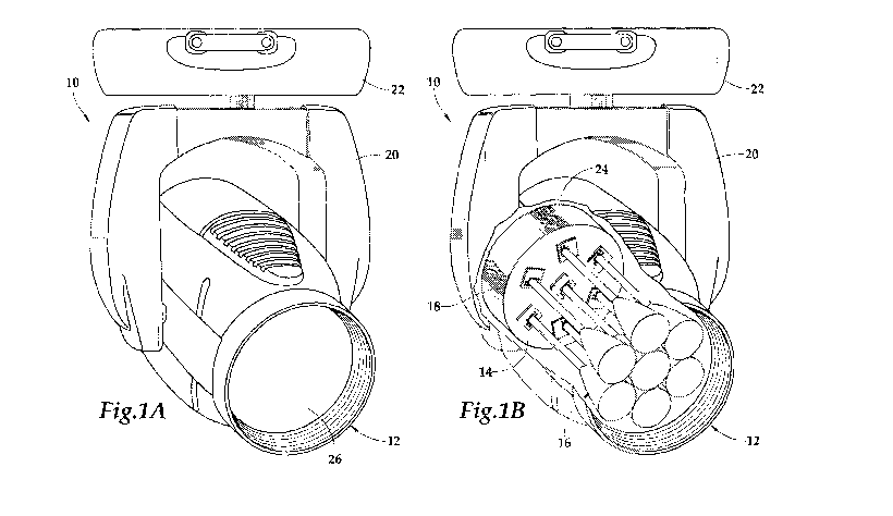
Figure IA is a perspective illustration of one embodiment of a luminaire
incorporating an
LED collimation optics module according to the teachings presented herein;
Figure 1B is a perspective illustration of the luminaire depicted in figure IA
with a
partial cut-away to better reveal internal components;
Figure 1C is a perspective illustration showing in further detail an array of
LED
collimation optics modules of figures IA and 113;
Figure 1D is a top plan view of the array of LED collimation optics modules
shown in
figure 1 C;
Figure 2 is a top plan view of another embodiment of an array of LED
collimation optics
modules;
Figure 3 is a top plan view of a further embodiment of an array of LED
collimation
optics modules;
Figure 4A is a front elevated view of one embodiment of an LED collimation
optics
module;
2
CA 027571962011-0&27
WO 2010/113100 PCT/IB2010/051354
Figure 4B is a transverse sectional view of the LED collimation optics module
illustrated
in figure 4A;
Figure 4C is a top plan view of the LED collimation optics module illustrated
in figure
4A;
Figure 4D is a top plan view of an LED chip package as viewed along line 4D -
4D of
figure 4A;
Figure 5A is a traverse sectional view of a single light beam traversing the
LED
collimation optics module illustrated in figure 4A;
Figure 5B is a traverse sectional view of a plurality of light beams
traversing the LED
collimation optics module illustrated in figure 4A;
Figure 6 is a traverse sectional view of a plurality of light beams traversing
another
embodiment of an LED collimation optics module;
Figure 7 is a traverse sectional view of a plurality of light beams traversing
a further
embodiment of an LED collimation optics module;
Figures 8-10 are top cross-sectional views of various embodiments of optical
conductors
for use with the LED collimation optics modules presented herein;
Figures 11-13 are top cross-sectional views of various embodiments of bodies
for use
with the LED collimation optics modules presented herein;
Figures 14-15 are top cross-sectional views of various embodiments of optical
conductors for use with the LED collimation optics modules presented herein;
Figures 16-17 are top cross-sectional views of various embodiments of CPCs for
use
with the LED collimation optics modules presented herein;
Figure 18 is a graph of intensity versus vertical angle representing a
baseline intensity for
the LED collimation optics module of figures 5A-5B;
Figure 19 is a graph of intensity versus vertical angle representing an
optimized baseline
intensity an LED collimation optics modules;
Figure 20 is a graph of intensity versus vertical angle representing a
baseline intensity for
a circular spaced-packing array of LED collimation optics modules;
Figure 21 is a graph of luminous efficiency and peak luminous flux versus
current
density for the circular spaced-packing array of LED collimation optics
modules;
3
CA 027571962011-0&27
WO 2010/113100 PCT/IB2010/051354
Figure 22 is an amber die chromaticity diagram with respect to the u', v'
color plane for
the circular spaced-packing array of LED collimation optics modules; and
Figure 23 is a white die chromaticity diagram with respect to the u', v' color
plane for
the circular spaced-packing array of LED collimation optics modules.
While the making and using of various embodiments of the present invention are
discussed in detail below, it should be appreciated that the present invention
provides many
applicable inventive concepts which can be embodied in a wide variety of
specific contexts. The
specific embodiments discussed herein are merely illustrative of specific ways
to make and use
the invention, and do not delimit the scope of the present invention.
Referring initially to figures IA through 1D, therein is depicted one
embodiment of a
luminaire according to the teachings presented herein that is schematically
illustrated and
generally designated 10. A housing 12 is adapted to accommodate a base 14 and
LED
collimation optics modules, collectively numbered 16, and secured within the
housing 12. The
LED collimation optics modules include individual LED collimation optics
modules 16-1, 16-2,
16-3, 16-4, 16-5, 16-6, and 16-7. A heatsink subassembly 18, which is also
mounted to the base
14 and enclosed in the housing 12, absorbs and dissipates heat produced by the
light emitting
diode collimation optics modules 16. In one embodiment, a one-to-one
correspondence is
present between the number of heatsinks and the number of light emitting diode
collimation
optics modules 16. Further, in one embodiment, the heatsink subassembly 18
includes virtually
silent fans that provide forced-air cooling for internal components including
the light emitting
diode collimation optics modules 16.
The housing 12 is fitted in place by a yoke 20 swivelly connected to a support
structure
22. An electronics subassembly 24 located throughout the housing 12, yoke 20,
and support
structure 22 provides motorized movement and electronics to the luminaire 10.
The electronics
subassembly 24 may include multiple on-board processors providing diagnostic
and self-
calibration functions as well as internal test routines and software update
capabilities. The
luminaire 10 may also include any other required electronics such as
connection to power. As
illustrated, a finishing lens 26 is included for adding end effects.
The LED collimation optics modules 16 are disposed in a single layer close-
packing
arrangement 28 with LED collimation optics modules 16-1 through 16-6 being
located in a
hexagonal positioning in contact with a centrally positioned optics module 16-
7. Each of the
4
CA 027571962011-0&27
WO 2010/113100 PCT/IB2010/051354
peripheral LED collimation optics modules 16-1 through 16-6 touches two
adjacent peripheral
LED collimation optics modules and the interiorly disposed LED collimation
optics module 16-
7. By way of example, the LED collimation optics module 16-1 touches adjacent
LED
collimation optics modules 16-2 and 16-6 as well as the collimation optics
module 16-7 located
in the interior. The array of the LED collimation optics modules 16-1 through
16-7 may have a
diameter of 8 inches (8.32 cm) in one embodiment. With respect to LED
collimation optics
module 16-4, an LED chip package 30 provides light to an optical conductor 32
that mixes the
light. A CPC 34 is coupled to the optical conductor 32 to collimate the light
received from the
optical conductor 32. Following collimation, light exits the luminaire 10 as a
substantially
homogenous pupil. Components of or the entirety of the luminaire 10 may be
considered an
optics module for stage lighting and related applications.
Figures 2 and 3 depict other embodiments of the LED collimation optics modules
16.
With respect to figure 2, the LED collimation optics modules 16 are positioned
in a single layer
circular spaced-packing arrangement 36. In this arrangement, the LED
collimation optics
modules 16-1 through 16-6 are respectively centered at peripheral points about
a centrally
positioned module, the LED collimation optics module 16-7. In one
implementation, the
spacing between the LED collimation optics modules 16 is approximately 0.19
inches (3 mm).
With respect to figure 3, the LED collimation optics modules 16-1 through 16-3
are
located in a linear single layer arrangement 38 wherein the interior LED
collimation optics
module 16-2 is disposed in contact with each of the exterior LED collimation
optics modules 16-
1, 16-3. It should be appreciated that the LED collimation optics modules may
be arranged in
arrays other than those illustrated in figures IA through 1D, figure 2, and
figure 3. Any number
of LED collimation optics modules may be utilized in an array and the array
may take different
forms including those providing for close contact between the LED collimation
optics modules
and those providing for space between the LED collimation optics modules and
even those that
provide for a combination thereof. Moreover, the LED collimation optics
modules 16 may be
arranged in an angular manner, linearly, or combinations thereof.
Figures 4A through 4D depict the LED collimation optics module 16-4. An LED
chip
package 30 provides sources of light and includes multiple colored LED chips
G, R, B, W
arranged in an array 42 on a single elongated base member 44, which may
include provisions for
bonding lead wires (not shown). As illustrated, the LED chips G, R, B, W have
been positioned
5
CA 027571962011-0&27
WO 2010/113100 PCT/IB2010/051354
to provide a desired angular emission pattern with respect to the optical
conductor 32 and CPC
34 to increase color mixing. It should be appreciated, however, that depending
on the
application, the LED chips G, R, B, W may be arranged in other types of
arrays.
The LED chips G, R, B, W of the array 42 comprise conventional green, red,
blue, and
white LED chips that respectively emit green, red, blue, and white light. Such
LED chips
facilitate efficient injection into the optical conductor 32 and strongly
enhance color mixing. As
depicted, in order to further enhance the quality of the white light generated
by the LED chip
package, four LED chips including one red LED chip (R), one green chip (G),
one blue LED
chip (B), and one white LED chip (W) are utilized. It is contemplated,
however, that as LED
chip design advances, different numbers of LED chips and/or different color
LED chips may be
used in the array to optimize the quality of the light generated by the LED
chip package 30. By
way of example, in one embodiment, four LED chips including one red LED chip
(R), one green
chip (G), one blue LED chip (B), and one amber LED chip (A) are utilized. By
way of further
example, in another embodiment, four LED chips including one red LED chip (R),
two green
chips (G1, G2), and one blue LED chip (B) are utilized. It is further
contemplated that both low-
power and high-power LED chips may be used in the LED chip package 30.
In one embodiment of the teachings presented herein, the elongated base member
44 may
comprise an electrically insulative housing 46, made for example, of plastic
or ceramic that
encases a metal heat sink with a silicon submount disposed thereon. The metal
heat sink
provides heat sinking to the LED chip package 30 disposed thereon. Further
heat dissipation is
provided by the heatsink subassembly 18 which, as alluded, includes a
virtually silent fan that
furnishes forced-air cooling proximate to the metal heat sink. The elongated
base member 44
may further include lead wires, which are electrically isolated from the metal
heat sink and the
LED chips G, R, B, W by the housing. Bond wires electrically connect the LED
chips G, R, B,
W to the lead wires.
The optical conductor 32 has at a first end an input aperture 48 of a cross-
sectional area
trig, wherein the radius is ri, and at a second end an output aperture 50 of a
second cross-
sectional area tr22, wherein the radius is r2. The optical conductor 32 is
superposed on the LED
chip package 30 and the LED chips G, R, B, W to receive the light from the
sources at the input
aperture 48 and deliver the light to the output aperture 50. The first cross-
sectional area 7Lr12
may be substantially equal to the second cross-sectional area 71r22 so that
the input aperture 48
6
CA 027571962011-0&27
WO 2010/113100 PCT/IB2010/051354
and output aperture 50 have substantially equal diameters and ri may equal r2.
A wall portion
52, which may be a cylindrical wall portion, connects the input aperture 48
with the output
aperture 50 and may include a surface of revolution generally forming a
cylinder. The wall
portion 52 includes a reflective material 54 defining multiple transmission
paths enabling
mixing of the light within an interior space 56 from the input aperture 48 to
the output aperture
50. In one implementation, the wall portion 52 may be a wall means for mixing
light connecting
the input aperture 48 with the output aperture 50. The length li of the
optical conductor 32 is
determined by design parameters related to the mixing of the light emitted by
the light sources.
Additionally, the length li of the optical conductor 32 is measured along a
longitudinal axis of
the optical conductor 32 which is substantially orthogonal to a horizontal
axis of the LED chip
package 30.
The CPC 34 is coupled to the optical conductor 32. With respect to the CPC 34,
a body
60, which in one embodiment is a conical body, is formed at a first end with
an entrance aperture
62 of a cross-sectional area rr32, wherein the radius is r3, and formed at a
second end with an
exit aperture 64 of a cross-sectional area tr42, wherein the radius is r3. The
entrance aperture 62
intersects the output aperture 50 and the conical body 60 is disposed to
deliver the light to the
exit aperture 64. The cross-sectional area rr32 of the entrance aperture 62 is
substantially equal
to the cross-sectional area rr22 of the output aperture 50 and the cross-
sectional area rr42 of the
exit aperture 64 is greater than the cross-sectional area rr32 of the entrance
aperture 62.
Accordingly, in this implementation, r4 > r3 = r2 = ri. A lip 72 at the second
end may have a
variety of forms including the illustrated arched edge which includes a
sequence of abutting
arches. This type of lip embodiment permits LED collimation optics modules to
be placed in
flush contact with one another in close-packing arrangements.
A wall portion 66, which may be a curved wall portion, connects the entrance
aperture
62 with the exit aperture 64 and diverges from the cross-sectional area 7Lr32
to the cross-sectional
area tr42. The wall portion 66 includes a reflective material 68 enabling
collimated transmission
of the light from the entrance aperture 62 to the exit aperture 64. The wall
portion 66 may be a
wall means connecting the entrance aperture 62 with the exit aperture 64 and
diverging from the
cross sectional area 7Lr32 to the cross-sectional area tr42. The wall portion
66 may include a
parabolic wall portion comprising a surface of revolution generally forming a
conical shape.
The length 12 of the CPC 34 is determined by design parameters related to the
desired
7
CA 027571962011-0&27
WO 2010/113100 PCT/IB2010/051354
collimation and degree of light mixing, for example. Additionally, the length
12 of the CPC 34 is
measured along a longitudinal axis of the CPC 34 which is substantially
aligned with the
longitudinal axis of the optical conductor 32 and orthogonal to the horizontal
axis of the LED
chip package 30. It should be appreciated that depending on the application,
the relationship
between the lengths 11 and 12 may vary from what is depicted.
In one embodiment, the CPC 34 is characterized by the fact that rays entering
the device
at its smaller aperture, the entrance aperture 62, are reflected only once
from an interior surface
to the curved wall portion 66 before exiting the CPC 34 at the larger
aperture, the exit aperture
64. In this implementation, the CPC 34 is designed to collimate a given of
flux of light of
energy received at the input aperture 62.
In this embodiment, the concentrator disclosed herein, which is termed a CPC
whether or
not the concentrator has a parabolic or other geometry, has a reflecting
material 68 made of a
prismatic, transparent, low-transmission loss dielectric material. As will be
discussed in figures
11-13, other geometries are within the embodiments presented herein. The
dielectric materials
from which the reflecting material 68 of an interior surface 70 of the CPC 34
may be made
include transparent polymers with a high index of refraction, such as, but no
limited to, acrylic
polymers or polycarbonate-based polymers.
Figure 5A depicts a single light beam traversing the LED collimation optics
module 16-
4. The optical conductor 32, which may be a light-mixing rod or lightpipe,
homogenizes the
light bundle transmitted therein by the light sources. The intensity centroid
of the light bundle
moves in a longitudinal fashion from the input aperture 48 to the output
aperture 50. The
reflecting surfaces of the reflecting material 54 disposed along the light-
mixing rod include
surface normals that are perpendicular or inclined relative to the
longitudinal or axial direction
of the movement of the light therethrough. The reflective material furnishing
pathways, such as
pathways 80, 82, for light beams to travel and thereby mix with each other.
The LED chips (G,
R, B, W) have at least a partial direction of orientation toward the interior
space 56 of the optical
conductor 32.
The CPC 34 is depicted in terms of a 0j/00j where 0i denotes the input angle
and Oo
denotes the output angle. The geometry of one embodiment may be better
understood by taking
a segment of parabola PR having its focal point Q and rotating this segment
around an axis of
revolution, which is at an angle 0i to the parabola's axis z, which is
perpendicular to the
8
CA 027571962011-0&27
WO 2010/113100 PCT/IB2010/051354
horizontal axis x through the LED chip package 30. The axis of rotation about
axis z defines the
center of the entrance aperture and the exit aperture. Such a CPC construction
is characterized
by the all rays of light entering at the input aperture at angles smaller than
+/- 0i with respect to
the axis z will exit the CPC after no more than a single reflection within the
angle of +/- Oo with
respect to the axis z.
As shown, light beams 84, 86 are transmitted from LED chip R of the LED chip
package
40. The angle of incidence from the light beam 84 is such that the light beam
84 does not
contact the interior space 56 of the optical conductor 32. In other
embodiments, due to the
location of the optical conductor 32, all or nearly all of the light beams
contact the interior
surface 56. The light beam 86, however, contacts the interior space 56 and
subsequently is
reflected from the reflective material 54 of the optical conductor 32 six
times before entering the
CPC 34 where the light beam 86 is collumated by a single reflection from the
interior surface 70
the CPC 34. As illustrated, the multiple reflections in the optical conductor
32 cause the light
beam 86 to cross the longitudinal axis z of the optical conductor 32, thereby
contributing to light
mixing.
Figure 5B depicts a plurality of beams traversing the LED collimation optics
module.
The optical conductor 32 superposed on the LED chip 30 to receive the light
from the sources of
LEDs G, R, B, W at the input aperture 48. The LEDs G-1, R, B, W are at least
partially oriented
toward the interior space 56 of the optical conductor 32. As shown, there is a
lateral offset
between the LEDs G, R, B, W to provide for an angle of incidence between the
LEDs and the
reflective material to furnish reflection therefrom. The optical conductor 32
provides multiple
pathways 89 that are traversed by multiple light beams, collectivelly light
bundle 88. The
multiple pathways 89 mix the received light beams and cause the intensity
centroid of the light
bundle 88 to move in a longitudinal fashion from the input aperture 48 to the
output aperture 50.
The reflective material of the optical conductor is oriented to propagate the
light from the input
aperture 48 to the output aperture 50 where the mixed light is received by the
CPC 34 at the
entrance aperture 62. Collimated transmission of the light from the entrance
aperture 62 to the
exit aperture 64 then occurs to produce a substantially homogenous pupil from
the single-
reflection, collimated transmission within the CPC 34. The light bundle exits
the exit aperture
64 as a substantially homogenous pupil 90.
9
CA 027571962011-0&27
WO 2010/113100 PCT/IB2010/051354
Figures 6 and 7 depict other embodiments of LED collimation optics modules.
With
reference to figure 6, an LED collimation optics module 16-8 produces a
substantially
homogenous pupil of light 92 having a different profile than the light
produced in figure 5. In
figure 7, an LED collimation optics module 16-9 having a combination of a
round polycarbonate
lightpipe 94 and an approximately 80% reflectivity within a hollow metalized
reflector identified
as CPC 96 produces another substantially homogenous pupil of light 98. It
should be
appreciated that construction of the of LED collimation optics modules
illustrated in figures 5A
through 7 may vary. For example, the optical conductors and CPCs may be
integrally formed or
bonded together to form integral units. Factors such as application specific
characteristics and
cost may determined the preferred construction technique.
Figures 8-10 depict various embodiments of optical conductors 32 for use with
LED
collimation optics modules 16. In figure 8, the optical conductor 32 comprises
the wall portion
52. It should be appreciated, however, that the optical conductors 32 are not
limited to
cylindrical wall portions. The optical conductors 32 may comprise non-
cylindrical shapes, as
well, that create different wall portions and respective interior spaces 56.
By way of example,
with reference to figure 9, the optical conductor 32 includes a faceted wall
portion having 6-
sides, which is indicated as hexagonal wall portion 100. By way of further
example, in figure
10, the optical conductor 32 comprises a wall portion having 8-sides, which is
indicated as an
octagon wall portion 102. The optical conductor 32 may include any number of
sides or facets
and it may further include circular or cylindrical wall portions.
Figures 11-13 depict various embodiments of bodies 60 of the CPCs 34. In one
implementation, the light emitting diode collimation optics module 16 is not
limited to the
conical body 60 having the curved wall portion 66 as shown in figure 11.
Rather, as shown in
figures 12 and 13, the light emitting collimation optics module 16 may include
a body having
any number of sides or facets, such as the body 60 of figure 12 and the body
60 of figure 13. In
these embodiments, rather than a curved wall portion, a wall portion having
sides or facets is
utilized, such as wall portions 104, 106, respectively presented in figures 12
and 13. The body
60 may include any number of sides or facets and it may further include the
aforementioned
curved wall portion.
Figures 14-15 depict embodiments of optical conductors 32 for use with the LED
collimation optics modules 16 presented herein. As previously discussed, the
optical conductor
CA 027571962011-0&27
WO 2010/113100 PCT/IB2010/051354
32 may take a variety of shapes. In addition to having a variety of shapes,
the optical conductor
32 may be a tubular or mixing tubular having a sidewall (e.g., figure 8), a
rod (e.g., figure 14), a
tubular having a body therein (e.g., figure 15), or a combination therefore,
for example. In
particular, with reference to figure 14, the optical conductor 32 is a rod
having wall portion 52
comprising the reflecting material 54. With reference to figure 15, the
optical conductor 32
includes a tubular member 32a having a body 32b therein and related wall
portions 52a, 54b and
reflective materials 54a, 54b.
Figures 16-17 depict embodiments of bodies 60 of CPCs 34 for use with the LED
collimation optics modules 16 presented herein. Similar to the optical
conductor 32, the bodies
60 of the CPCs 34 may have a variety of forms including the body 60 having a
sidewall (e.g.,
figure 11), the body 60 being a solid member (e.g., figure 16) with the wall
portion 66 and
reflective material 68, the body 60 having a sidewall member 60a and a solid
member 60b
disposed therein (e.g., figure 17) with wall portions 66a, 66b and the
reflective materials 68a,
68b, or combinations thereof, for example.
Figure 18 depicts a graph of intensity versus vertical angle representing
baseline
intensity for a single layer close-packing arrangement having hexagonal
positioning. Herein the
vertical angle of light incidence is expressed in degrees and intensity as
shown by line 110.
Figure 19 depicts a graph of intensity versus vertical angle representing a
baseline intensity for a
hexagonal array of light emitting diode collimation optics modules. A line 120
expresses the
relationship between intensity and vertical angle. In this embodiment, the
optimized baseline
intensity model produces the narrowest angular distribution possible while not
compromising
color uniformity. The angular distribution of this model may be reduced
further by reducing the
size of the lightpipe input plane or increasing the lightpipe output plane.
Lastly, figure 20
depicts a graph of intensity versus vertical angle representing a baseline
intensity for a single
layer circular spaced-packing arrangement of light emitting diode collimation
optics modules.
In this figure, a line 130 shows the relationship of intensity versus vertical
angle. The designs
represented by the graphs exceed luminous flux requirements of 10,000 lumens.
The Hex +
CPC embodiment (figure 18) being 69% efficient with better color uniformity
and the Round +
Hollow CPC (figure 20) reflector embodiment being 49% efficient with a two
piece approach
that includes a round polycarbonate lightpipe with hollow metalized CPC
reflector.
11
CA 027571962011-0&27
WO 2010/113100 PCT/IB2010/051354
Figure 21 is a graph showing the relative luminous efficiency as well as the
peak
luminous flux as a function of a current density. A line 140 of luminous
efficiency expresses the
ratio of luminous flux to radiant flux in lumen per Watts (lm/W) as a function
of current density
(A/mm2). Additionally, a line 150 of peak luminous flux expresses the luminous
flux in lumen
(1m) as a function of current density (A/mm2).
Figure 22 depicts an amber die chromaticity diagram with respect to the u', v'
colorimetry color space coordinates for a rounded array of light emitting
diode collimation
optics modules having the single layer circular spaced-packing arrangement
previously
discussed. The depicted CIELUV color space, CIE 1976 (L*, u*, V*) is an Adams
chromatic
valence color space, and is an update of the CIE 1964 color space (CIEUVW).
The differences
include a slightly modified lightness scale, and a modified uniform
chromaticity scale (for
example, in which one of the coordinates, v', is 1.5 times as large as v, its
1960 predecessor).
The displayed wavelengths are expressed in nanometers (nm).
The following conversions and transformations are applicable:
L* = 116(Y/Yõ)v3 - 16, Y/Yõ > (6/29)3
(29/3)3(Y/Yõ), Y/Yn <= (6/29)3
U* = 13L*(u' - u'õ)
V* = 13L*(v' - v'õ)
u' = 4X(X + 15Y + 3Z) = 4x/(-2x + 12y + 3)
v' = 9Y(X + 15Y +3Z) = 9Y/(-2x + 12Y + 3)
With the respect to the transformation from (u',v') to (x,y) is:
x = 9u'/(6u' - 16v' + 12)
y = 4v'/(6u' - 16v' + 12)
u' = u*/13L* + u'õ
v' = v*/13L* + v'õ
Y = Y L*(3/29)3, L* <= 8
Yõ(L* + 16)/116)3, L* > 8
X = Y(9u'/4v')
Z = Y((12 - 3u' - 20v')/4v')
12
CA 027571962011-0&27
WO 2010/113100 PCT/IB2010/051354
The turned-U shaped locus boundary 160 represents monochromatic light, or
spectral
colors or loosely rainbow colors. The lower-bound of the locus presents the
line of purples and
represents non-spectral colors obtained by mixing light of red and blue
wavelengths. It should
be understood that in reality this boundary is not hard, as the colors just
become dimmer and
dimmer owing to the falloff in sensitivity of the receptors of the eye at the
extreme ends of the
visible spectrum. Colors on the periphery of the locus are saturated and
colors become
progressively desaturated and tend towards white somewhere in the middle of
the plot. Colors
outside of the plot are out-of-gamut, however, the chromaticity diagram is not
perceptually
uniform. That is to say the area of any region of the plot may not correlate
at all well with the
number of perceptually-distinguishable colors in that region. Further,
different light LED
sources may have inherently different color gamuts.
Figure 23 depicts a white die chromaticity diagram with respect to the u', v'
colorimetry
color space coordinates for a rounded array of light emitting diode
collimation optics modules
having the single layer circular spaced-packing arrangement. Similar to figure
22, the displayed
wavelengths are expressed in nanometers (nm) and the turned-U shaped locus
boundary 170
represents monochromatic light. As illustrated, the turned-U shaped locus
boundary 160
represents deviations in u', v' that are indistinguishable to the human eye
and average
chromaticity values are in the order of 0.06.
While this invention has been described with reference to illustrative
embodiments, this
description is not intended to be construed in a limiting sense. Various
modifications and
combinations of the illustrative embodiments as well as other embodiments of
the invention,
will be apparent to persons skilled in the art upon reference to the
description. It is, therefore,
intended that the appended claims encompass any such modifications or
embodiments.
13