Note: Descriptions are shown in the official language in which they were submitted.
110355:910592
DESCRIPTION
TITLE OF INVENTION
Method of Manufacturing Single Crystal
TECHNICAL FIELD
The present invention relates to a method of manufacturing a single crystal,
and
in particular to a method of manufacturing a single crystal using a seed
crystal fixed on a
pedestal.
BACKGROUND ART
In recent years, silicon carbide single crystal substrates have been adopted
as
semiconductor substrates for use in manufacturing semiconductor devices.
Silicon
carbide has a band gap larger than that of silicon, which has been used more
commonly
in the field of semiconductor. Hence, a semiconductor device employing silicon
carbide advantageously has a large reverse breakdown voltage, low on-
resistance, and
has properties less likely to decrease in a high temperature environment.
A silicon carbide single crystal is manufactured using a sublimation-
recrystallization method. Specifically, a silicon carbide single crystal is
grown on a
surface of a seed crystal fixed on a pedestal. If the seed crystal is not
uniformly fixed
on the pedestal, the single crystal grown on the seed crystal may have a
reduced quality.
Thus, as a method of mounting the seed crystal to the pedestal, for example,
the
following two methods have been proposed.
Firstly, according to Japanese Patent Laying-Open No. 2001-139394 (Patent
Literature 1), when a single crystal is grown, a carbon composite structure
having
graphite fine particles and non-graphitizable carbon is formed in an interface
between a
seed crystal and a seed crystal pedestal. This publication describes that,
since carbon is
thereby uniformly formed all over an attachment surface using heat-resistant
fine
particles uniformly dispersed in the attachment surface as cores, and covers
an
attachment surface of the seed crystal, it is possible to prevent occurrence
of
-1-
110355: 910592
recrystallization in the attachment surface of the seed crystal to be attached
to the
pedestal during growth of the single crystal, and it is also possible to
prevent etching
which may occur at a central portion of the seed crystal in an early stage of
the growth.
Secondly, according to Japanese Patent Laying-Open No. 2003-226600 (Patent
Literature 2), a silicon carbide seed crystal having a protective film with a
thickness of
0.5 to 5 .tm formed on a backside surface thereof is mechanically mounted on a
graphite
crucible lid. This publication describes that, since the protective film can
prevent
sublimation of Si atoms from the backside surface of the seed crystal,
generation of
voids in a crystal is suppressed.
CITATION LIST
PATENT LITERATURE
PTL 1: Japanese Patent Laying-Open No. 2001-139394
PTL 2: Japanese Patent Laying-Open No. 2003-226600
SUMMARY OF INVENTION
TECHNICAL PROBLEM
In the technique of Japanese Patent Laying-Open No. 2001-139394 (Patent
Literature 1), there has been a possibility that strength of fixing between
the seed crystal
and the pedestal may be insufficient, depending on the material for the seed
crystal. In
particular, if the temperature between the seed crystal and the pedestal is
set to a high
temperature as in the case where, for example, a silicon carbide single
crystal is grown,
the strength of fixing described above has been likely to be reduced.
Therefore, there
has been a possibility that a portion or all of the seed crystal may be
detached from the
pedestal. Hence, there has been a possibility that the quality of the obtained
single
crystal may be reduced.
As to the technique of Japanese Patent Laying-Open No. 2003-226600 (Patent
Literature 2), the present inventors have found as a result of examination
that protection
of the backside surface of the seed crystal is insufficient. For example, if a
silicon
carbide seed crystal is used, the effect of preventing sublimation of the
backside surface
-2-
110355:910592
of the seed crystal is not sufficient, and as a result, there has been a
possibility that the
quality of the obtained single crystal may be reduced.
The present invention has been made in view of the aforementioned problem,
and one object of the present invention is to provide a method of
manufacturing a single
crystal capable of growing a high-quality single crystal using a seed crystal
fixed on a
pedestal.
SOLUTION TO PROBLEM
A method of manufacturing a single crystal according to one aspect of the
present invention includes the steps of. preparing a seed crystal having a
frontside
surface and a backside surface; increasing surface roughness of the backside
surface of
the seed crystal; forming a coating film including carbon on the backside
surface of the
seed crystal after the surface roughness is increased; bringing the coating
film and a
pedestal into contact with each other with an adhesive interposed
therebetween; curing
the adhesive to fix the seed crystal to the pedestal; and growing the single
crystal on the
seed crystal. Before the growth is performed, a carbon film is formed by
carbonizing
the coating film.
A method of manufacturing a single crystal in accordance with another aspect
of
the present invention includes the steps of. preparing a seed crystal having a
frontside
surface and a backside surface, the backside surface being an as-sliced
surface formed by
slicing with a wire saw; forming a coating film including carbon on the
backside surface
of the seed crystal; bringing the coating film and a pedestal into contact
with each other
with an adhesive interposed therebetween; curing the adhesive to fix the seed
crystal to
the pedestal; and growing the single crystal on the seed crystal fixed to the
pedestal.
Before the growth is performed, a carbon film is formed by carbonizing the
coating film.
Preferably, the step of increasing the surface roughness of the backside
surface is
performed by treating the backside surface using abrasive grains. More
preferably,
grain size distribution of the abrasive grains has a component of not less
than 16 m.
Preferably, the coating film is an organic film, and the carbon film is formed
by
-3-
110355:910592
carbonizing the organic film. More preferably, the organic film is formed of
an organic
resin. Further preferably, the organic resin is a photosensitive resin.
Preferably, the step of forming the coating film is performed using spin
coating.
In addition, preferably, the pedestal is polished prior to the step of
bringing the coating
film and the pedestal into contact with each other with the adhesive
interposed
therebetween.
Preferably, the adhesive includes a resin which will become non-graphitizable
carbon by being heated, heat-resistant fine particles, and a solvent. More
preferably,
the adhesive includes a carbohydrate.
Preferably, the single crystal is a silicon carbide single crystal. In
addition,
preferably, a surface of the pedestal facing the seed crystal includes a
surface made of
carbon.
ADVANTAGEOUS EFFECTS OF INVENTION
According to the method of manufacturing a single crystal in accordance with
the present invention, when growth of a single crystal is performed, a carbon
film is
provided on the backside surface of the seed crystal, and since the carbon
film is made
of carbon, it is firmly and uniformly bonded with the cured adhesive. Further,
since the
carbon film is formed on the backside surface of the seed crystal as a surface
having an
increased surface roughness, with high adhesiveness. That is, the carbon film
is firmly
bonded to each of the adhesive and the seed crystal. Therefore, the seed
crystal is
firmly and uniformly fixed to the pedestal with the adhesive interposed
therebetween,
and thus the single crystal grown on the seed crystal has an improved quality.
BRIEF DESCRIPTION OF DRAWINGS
Fig. 1 is a cross sectional view schematically showing a first step of a
method of
manufacturing a single crystal according to one embodiment of the present
invention.
Fig. 2 is a cross sectional view schematically showing a second step of the
method of manufacturing a single crystal according to one embodiment of the
present
invention.
-4-
110355:910592
Fig. 3 is a cross sectional view schematically showing a third step of the
method
of manufacturing a single crystal according to one embodiment of the present
invention.
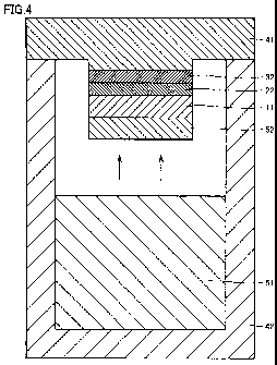
Fig. 4 is a cross sectional view schematically showing a fourth step of the
method of manufacturing a single crystal according to one embodiment of the
present
invention.
Fig. 5 is a cross sectional view showing one step of a method of manufacturing
a
single crystal according to a first comparative example.
Fig. 6 is a cross sectional view showing one step of a method of manufacturing
a
single crystal according to a second comparative example.
DESCRIPTION OF EMBODIMENTS
Hereinafter, an embodiment of the present invention will be described with
reference to the drawings.
Referring to Fig. 1, a seed crystal 11 is prepared. Seed crystal 11 has a
frontside surface (lower surface in the drawing) as a surface on which a
single crystal
will grow, and a backside surface (upper surface in the drawing) as a surface
to be
mounted to a pedestal. For example, seed crystal 11 is formed of silicon
carbide (SiC).
Seed crystal 11 has a thickness (dimension in the vertical direction in the
drawing) of,
for example, not less than 0.5 mm and not more than 10 mm. In addition, the
planar
shape of seed crystal 11 is, for example, a circle, and the diameter thereof
is preferably
not less than 25 mm, and more preferably not less than 100 mm. Further, the
tilt of the
plane orientation of the seed crystal from the (0001) plane, that is, the off
angle, is
preferably not more than 15 , and more preferably not more than 5 .
Next, treatment to further increase surface roughness of the backside surface
of
seed crystal 11 is performed. This treatment can be performed by polishing the
backside surface using abrasive grains having a sufficiently large grain size.
Preferably,
grain size distribution of the abrasive grains has a component of not less
than 16 m.
An average grain size of the abrasive grains is preferably not less than 5 m
and not
more than 50 m, more preferably not less than 10 m and not more than 30 m,
and
-5-
110355:910592
further preferably 12 to 25 m.
Preferably, the abrasive grains described above are diamond particles. In
addition, preferably, the abrasive grains described above are used in a state
dispersed in
slurry. Thus, the polishing described above is preferably performed using
diamond
slurry. Generally, diamond slurry containing diamond particles which have an
average
grain size of not less than 5 m and not more than 50 m and whose grain size
distribution has a component of not less than 16 .im is easily available.
It is to be noted that, instead of performing treatment to further increase
surface
roughness of the backside surface of seed crystal 11 as described above, it is
also
possible to form a backside surface originally having a sufficiently large
surface
roughness and use the backside surface without polishing it. Specifically, the
backside
surface of seed crystal 11 formed by slicing with a wire saw may be used
without being
polished. That is, an as-sliced surface, which is a surface formed by slicing
and not
polished thereafter, may be used as the backside surface. Preferably, the
abrasive
grains described above are used for the slicing with a wire saw.
Next, a coating film 21 including carbon is formed on the backside surface of
seed crystal 11. Preferably, coating film 21 has a surface roughness smaller
than that of
the backside surface of seed crystal 11 on which coating film 21 is formed.
Preferably, this formation is performed by applying a liquid material, and
more
preferably, the liquid material does not contain a solid such as fine
particles. Thereby,
thin coating film 21 can be formed easily and uniformly.
In the present embodiment, coating film 21 is an organic film. Preferably, the
organic film is formed of an organic resin. As the organic resin, for example,
various
resins such as an acrylic resin, a phenolic resin, a urea resin, and an epoxy
resin can be
used, and a resin composed as a photosensitive resin that is cross-linked or
decomposed
by action of light can also be used. As the photosensitive resin, a positive
or negative
photoresist used for manufacturing semiconductor devices can be used. Since
the
technique of applying these materials by spin coating has already been
established, the
-6-
110355: 910592
thickness of coating film 21 can be easily controlled. Spin coating is
performed, for
example, as described below.
Firstly, seed crystal 11 is suctioned onto a holder. Seed crystal 11 is
rotated by
rotating the holder at a prescribed rotation speed. A photoresist is dropped
on rotating
seed crystal 11, and thereafter rotation is continued for a prescribed time
period to apply
the photoresist thinly and uniformly. To ensure uniformity over an entire
surface of
seed crystal 11, for example, the rotation speed is set to 1000 to 10000
rotations/minute,
the time period is set to 10 to 100 seconds, and the application thickness is
set to not
less than 0.1 m.
Then, the applied photoresist is dried and thereby cured. The drying
temperature and the drying time period can be selected as appropriate
depending on the
material for the photoresist and the application thickness thereof.
Preferably, the
drying temperature is not less than 100 C and not more than 400 C, and the
drying time
period is not less than 5 minutes and not more than 60 minutes. For example,
when the
drying temperature is 120 C, the time period required for volatilization is,
for example,
15 minutes for a thickness of 5 m, 8 minutes for a thickness of 2 m, and 3
minutes for
a thickness of 1 m.
It is to be noted that, although coating film 21 can be formed if the step of
applying and drying the photoresist described above is performed once, thicker
coating
film 21 may be formed by repeating this step. Since repeating this step too
many times
is not preferable as it takes time more than necessary for this step, it is
generally
preferable to limit the number of repetitions to about two or three.
Referring to Fig. 2, a pedestal 41 having a mounting surface on which seed
crystal 11 is to be mounted is prepared. The mounting surface includes a
surface
preferably made of carbon. For example, pedestal 41 is formed of graphite.
Preferably, the mounting surface is polished to improve flatness of the
mounting surface.
Next, coating film 21 and pedestal 41 are brought into contact with each
other,
with an adhesive 31 interposed therebetween. Preferably, the contact is
performed
-7-
110355:910592
such that the both press against each other at a temperature of not less than
50 C and
not more than 120 C, and under a pressure of not less than 0.01 Pa and not
more than 1
MPa. Further, if adhesive 31 is applied so as not to spread out of a region
sandwiched
between seed crystal 11 and pedestal 41, an adverse effect of adhesive 3 1 in
the step of
growing a single crystal using seed crystal 11 described later can be
suppressed.
Preferably, adhesive 31 includes a resin which will become non-graphitizable
carbon by being heated and thereby carbonized, heat-resistant fine particles,
and a
solvent. More preferably, adhesive 3 1 further includes a carbohydrate.
The resin which will become non-graphitizable carbon is, for example, a
novolak
resin, a phenol resin, or a furfuryl alcohol resin.
The heat-resistant fine particles have a function of uniformly distributing
the non-
graphitizable carbon described above in a fixing layer formed by heating
adhesive 31 to a
high temperature, and thereby increasing the filling rate of the fixing layer.
As a
material for the heat-resistant fine particles, a heat-resistant material such
as carbon (C)
including graphite, silicon carbide (SiC), boron nitride (BN), and aluminum
nitride (AIN)
can be used. In addition, a high melting point metal, or a compound such as a
carbide
or a nitride thereof can also be used as a material other than those described
above. As
the high melting point metal, for example, tungsten (W), tantalum (Ta),
molybdenum
(Mo), titanium (Ti), zirconium (Zr), or hafnium (Hf) can be used. The heat-
resistant
fine particles have a grain size of, for example, 0.1 to 10 m.
As the carbohydrate, a saccharide or a derivative thereof can be used. The
saccharide may be a monosaccharide such as glucose, or a polysaccharide such
as
cellulose.
As the solvent, a solvent that can dissolve and disperse the resin and the
carbohydrate described above is selected as appropriate. Further, the solvent
is not
limited to a solvent composed of a single type of liquid, and may be a mixed
liquid
containing plural types of liquids. For example, a solvent including alcohol
for
dissolving the carbohydrate and cellosolve acetate for dissolving the resin
may be used.
-8-
110355:910592
The ratio among the resin, the carbohydrate, the heat-resistant fine
particles, and
the solvent in adhesive 31 is selected as appropriate to obtain suitable
adhesion and
fixing strength of seed crystal 11. In addition, the components of adhesive 31
may
include a component other than those described above, and may include, for
example, an
additive such as a surfactant, a stabilizer, and the like. Further, the
application amount
of adhesive 31 is preferably not less than 10 mg/cm2 and not more than 100
mg/cm2.
Furthermore, the thickness of adhesive 31 is preferably not more than 100 m,
and more
preferably not more than 50 m.
Next, preferably, adhesive 31 is prebaked. Preferably, the prebaking is
performed at a temperature of not less than 150 C.
Further, referring to Fig. 3, coating film 21 and adhesive 31 (Fig. 2) are
heated.
As a result of the heating, coating film 21 is carbonized and becomes a carbon
film 22.
That is, carbon film 22 is formed on seed crystal 11. Further, as a result of
the heating,
adhesive 31 is cured between carbon film 22 and pedestal 41, and becomes a
fixing layer
32. Thereby, seed crystal 11 is fixed to pedestal 41.
Preferably, the heating described above is performed at a temperature of not
less
than 800 C and not more than 1800 C, for a time period of not less than one
hour and
not more than 10 hours, under a pressure of not less than 0.13 kPa and not
more than
the atmospheric pressure, and in an inactive gas atmosphere. As an inactive
gas, for
example, helium, argon, or nitrogen gas is used.
Referring to Fig. 4, a source material 51 is placed inside a crucible 42. If a
single crystal to be grown is formed of SiC, for example, SiC powder is placed
in a
graphite crucible. Then, pedestal 41 is mounted such that seed crystal 11
faces the
inside of crucible 42. It is to be noted that pedestal 41 may function as a
lid for
crucible 42 as shown in Fig. 4.
Subsequently, a single crystal 52 is grown on seed crystal 11. In the case
where
SiC single crystal 52 is manufactured using SiC seed crystal 11, the
sublimation-
recrystallization method can be used as a forming method therefor.
Specifically, single
-9-
110355:910592
crystal 52 can be grown by subliming source material 51 as indicated by arrows
in the
drawing, and depositing a sublimate on seed crystal 11. The temperature in the
sublimation-recrystallization method is set, for example, to not less than
2100 C and not
more than 2500 C. Further, the pressure in the sublimation-recrystallization
method is
preferably set, for example, to not less than 1.3 kPa and not more than the
atmospheric
pressure, and more preferably set to not more than 13 kPa to increase a growth
rate.
It is to be noted that, when this growth is performed, coating film 21 (Fig.
2) has
already become carbon film 22 (Fig. 3), as already described using Figs. 2 and
3.
Referring to Fig. 5, in a first comparative example, seed crystal 11 is bonded
to
pedestal 41 using fixing layer 32, without carbon film 22 (Fig. 3) interposed
therebetween. In the present comparative example, strength of fixing between
seed
crystal 11 and pedestal 41 may be insufficient, depending on the material for
seed crystal
11. Particularly, if the temperature between seed crystal 11 and pedestal 41
is set to a
high temperature as in the case where, for example, a SiC single crystal is
grown by the
sublimation-recrystallization method, the strength of fixing described above
is likely to
be reduced. For example, an adhesion strength obtained by a fixing layer
formed by
curing a carbon-based adhesive is likely to be reduced under a temperature of
about
2000 C generally used to grow SiC. As a result, a portion or all of seed
crystal 11 may
be detached from the pedestal, and thus the quality of the obtained single
crystal may be
reduced. Further, in this case, while seed crystal 11 is often formed of SiC,
and
pedestal 41 is often formed of graphite, it is difficult to firmly fix the
both using fixing
layer 32 due to material properties of the both. For example, although the
fixing layer
formed by curing a carbon-based adhesive can bond carbon materials (graphites)
with
high strength, the fixing layer cannot bond a carbon material and SiC with a
comparable
strength.
In contrast, according to the present embodiment, carbon film 22 is provided
on
seed crystal 11, and fixing layer 32 fixes carbon film 22 to pedestal 41. That
is, fixing
layer 32 is joined to carbon film 22, not to seed crystal 11. Thereby, bonding
is
- 10-
110355: 910592
performed without directly depending on the material for seed crystal 11, and
thus seed
crystal 11 and pedestal 41 can be fixed more firmly. In particular, when
pedestal 41 is
formed of carbon such as graphite, carbon film 22 can be firmly bonded to
pedestal 41
using the carbon-based adhesive as they are both formed of carbon.
Further, the surface roughness of the backside surface of seed crystal 11 is
increased before coating film 21 is formed on the backside surface of seed
crystal 11.
This can increase adhesiveness between carbon film 22 formed by carbonizing
coating
film 21 and the backside surface of seed crystal 11.
In addition, preferably, coating film 21 has a surface roughness smaller than
that
of the backside surface of seed crystal 11 on which coating film 21 is formed.
Since
this can reduce asperities in the surface to be bonded to pedestal 41, this
can prevent
occurrence of a portion in which bonding to the pedestal is locally
insufficient.
Referring to Fig. 6, in a second comparative example, seed crystal 11 provided
with carbon film 22 with a thickness of 0.5 to 5 p.m is fixed to pedestal 41
using a
mechanical fixture 33. In the present comparative example, there may occur a
gap
between seed crystal 11 and pedestal 41, specifically in an interface between
carbon film
22 and pedestal 41, due to a difference in thermal expansion coefficient
between the
material for seed crystal 11 and the material for pedestal 41. If temperature
distribution occurs within a growth surface of seed crystal 11 in accordance
with
distribution of the gap, a uniform single crystal cannot be obtained. In
addition, if a
material transfers from seed crystal 11 into the gap due to sublimation or the
like,
composition distribution occurs within the growth surface of seed crystal 11,
and as a
result, there may occur a case where a uniform single crystal cannot be
obtained. In
particular, if seed crystal 11 is formed of SiC, Si may transfer into the gap,
and the
transfer cannot be fully suppressed by carbon film 22 with a thickness of
about 0.5 to 5
m. Consequently, seed crystal 11 has a Si-deficient region, and a micropipe
defect
may occur in a portion of the single crystal formed on seed crystal 11 which
is located
on this region.
-11-
110355:910592
In contrast, according to the present embodiment, seed crystal 11 is fixed not
by
a mechanical jig but by firm and uniform joining between carbon film 22 and
fixing layer
32. Thus, since the gap as described above is less likely to be generated,
occurrence of
composition distribution and temperature distribution in seed crystal 11 is
suppressed,
and thereby single crystal 52 can be manufactured more uniformly. It is to be
noted
that the temperature distribution can be further suppressed by polishing the
mounting
surface of pedestal 41.
Although a crystal formed of SiC has been described above as seed crystal 11,
a
crystal formed of another material may be used. As a material therefor, for
example,
GaN, ZnSe, ZnS, CdS, CdTe, AIN, or BN can be used.
Further, although coating film 21 is carbonized when adhesive 31 is cured in
the
present embodiment, coating film 21 may be carbonized before adhesive 31 is
formed.
In addition, single crystal 52 may be used to manufacture a substrate such as
a
SiC substrate. Such a substrate is obtained, for example, by slicing single
crystal 52.
[Examples]
(Example 1)
Referring to Fig. 1, a SiC substrate having a thickness of about 3 mm, a
diameter
of 60 mm, a polytype of 4H, and a plane orientation of (000-1) was prepared as
seed
crystal 11. A backside surface of seed crystal 11 was mechanically polished
using
diamond slurry having a grain size of about 15 pm.
Next, seed crystal 11 was mounted on a holder such that the backside surface
of
seed crystal 11 was exposed. Then, while seed crystal 11 was rotated by
rotating the
holder at 1450 rotations/minute, a resist liquid containing ethyl lactate and
butyl acetate
was dropped on the backside surface by about 20 mmg using a dropper, and
thereafter,
rotation was continued for 20 seconds. Thereby, the resist liquid was applied
with a
thickness of about 1 .tm. Subsequently, drying was performed at 350 C for 20
minutes,
and thus coating film 21 was formed.
Referring to Fig. 2, graphite pedestal 41 having a mounting surface on which
-12-
110355: 910592
seed crystal 11 was to be mounted was prepared. Then, the mounting surface was
polished using diamond slurry.
Next, adhesive 31 including a phenol resin, phenol, ethyl alcohol,
formaldehyde,
water, and a solid carbon component was prepared. Coating film 21 and pedestal
41
were brought into contact with each other, with adhesive 31 interposed
therebetween.
Adhesive 31 was applied in an amount of about 25 mg/cm2, with a thickness of
about 40
m. The contact was performed under conditions of a temperature of 100 C and a
pressure of 0.1 MPa.
Subsequently, adhesive 31 was prebaked. Specifically, heat treatment at 80 C
for four hours, heat treatment at 120 C for four hours, and heat treatment at
200 C for
one hour were successively performed.
Next, coating film 21 and adhesive 31 were heated. This heating was
performed at 1150 C for one hour in a helium gas atmosphere at 80 kPa. Coating
film
21 and adhesive 31 were carbonized by this heating, and thereby carbon film 22
and
fixing layer 32 (Fig. 3) both made of carbon were formed.
Referring to Fig. 4, SiC powder as source material 51 was placed inside
graphite
crucible 42. Next, pedestal 41 was mounted such that seed crystal 1 l faced
the inside
of crucible 42 and pedestal 41 functioned as a lid for crucible 42.
Subsequently, SiC single crystal 52 was grown on seed crystal 11 by the
sublimation-recrystallization method. SiC single crystal 52 was grown at a
temperature
of 2400 C and a pressure of 1.7 kPa, for 300 hours.
Next, the obtained SiC single crystal 52 was sliced to obtain a SiC substrate.
As a result of evaluating a surface of the SiC substrate, it had a void
density of 0/cm2
and a micropipe density of 1/cm2.
(Example 2)
Although the backside surface of the seed crystal was polished using diamond
slurry having a grain size of 15 m in the example described above, diamond
slurry
whose grain size distribution had a component with a grain size of not less
than 16 m
- 13 -
110355:910592
was used in the present example. According to the present example,
adhesiveness
between the backside surface of seed crystal 11 and carbon film 22 was further
increased.
(Comparative Examples)
In the case of the first comparative example (Fig. 5), seed crystal 11 fell
from
pedestal 41 with a probability of one third while the temperature was
increasing to
perform the sublimation-recrystallization method or while the single crystal
was growing.
When a surface of a SiC substrate obtained in the case where the falling did
not occur
was evaluated, it had a void density of 10/cm2 and a micropipe density of
50/cm2.
In the case of the second comparative example (Fig. 6), when a surface of an
obtained SiC substrate was evaluated, it had a void density of 120/cm2 and a
micropipe
density of 300/cm2.
It should be understood that the embodiment and examples disclosed herein are
illustrative and non-restrictive in every respect. The scope of the present
invention is
defined by the scope of the claims, rather than the description above, and is
intended to
include any modifications within the scope and meaning equivalent to the scope
of the
claims.
REFERENCE SIGNS LIST
11: seed crystal, 21: coating film, 22: carbon film, 31: adhesive, 32: fixing
layer,
33: fixture, 41: pedestal, 42: crucible, 51: source material, 52: single
crystal.
-14-