Note: Descriptions are shown in the official language in which they were submitted.
CA 02759946 2011-11-29
SINGLE WIRE BUS SYSTEM
Field
The present disclosure is generally directed at bus systems and more
specifically at a
single wire bus system.
Background
In a computer or processor architecture, a bus is a subsystem that transfers
data
between computer components within a computer or between computers. Bus
architectures are also used in common data signalling paths for multiple
devices, rather
than having separate connections between each set of devices that need to
communicate.
In other words, the bus structure can be used to allow one or more slave
devices to
communicate with one or more master devices.
Brief Description of the Drawings
Embodiments of the present disclosure are now described, by way of example
only, with reference to the attached Figures, wherein:
Figure 1 is a perspective view of a portable electronic device;
Figure 2 is a block diagram of a portable electronic device;
Figure 3 is a schematic diagram of a single wire bus system;
Figure 4a is a schematic diagram of a timing diagram;
Figure 4b is a schematic timing diagram of sixteen clock cycles;
Figure 4c is a diagram of a single time frame;
Figure 4d is a diagram of part of a Y word;
Figures 4e to 4g are schematics of example clock signals;
Figure 5 is a schematic diagram of a timing diagram;
Figure 6 is a schematic diagram of an interface control register;
Figure 7 is a schematic diagram of an IRQ mask;
Figure 8 is a schematic diagram of a status register;
Figure 9 is a schematic diagram of how a sync word is transmitted;
Figure 10a is a schematic diagram of an X word in ping operation;
Figure 10b is a schematic diagram of an Y word in ping operation;
Figure lla is a schematic diagram of an X word for read operations;
1
CA 02759946 2011-11-29
Figure lib is a schematic diagram of a Y word for read operations;
Figure 12a is a schematic diagram of an X word for write operations;
Figure 12b is a schematic diagram of a Y word for write operations; and
Figures 13a to 13e are schematic diagrams of example time frames.
Detailed Description
A single bus architecture is described below as a system that communicates
over a
single wire, and comprises sync, control, data, clock and power over this
transmission
media. The bus may be used for operation where the number of pins or wires is
limited or
where high reliability with respect to noise immunity is desired. The bus of
the current
disclosure preferably allows continuous operation of a number of external
devices and that
all devices are synchronized by the same clock signal.
The single bus architecture may be based on a continuous clock source charging
a wire, a
PCB trace or a transmission line, and allows a variable number of receivers,
such as slave
devices, to discharge the line at specified time instants in order to provide
a
communication link. If the system clock frequency is low, a bus holder may be
added to
the system to maintain the charge on the wire.
The disclosure is directed at a single bus architecture for communication
between
at least two devices, such as master and slave devices. Transmission between
the master
and slave devices include a continuous clock system and bi-directional data.
In bus architectures, there is often a mechanism for devices to signal when
they
need to use the bus, while it is in use, and the nature of the use, such as
for data, the
transmission of instructions, the transmission of control information or
signals. etc.,
however, bus control can become quite complicated when numerous asynchronous
processes are attempting to share the bus efficiently. Systems usually require
multiple
wires and bonding pads which results in a system with a higher cost. When such
systems
are used with external devices, multiple connectors are also needed resulting
in larger
space requirements.
Turning to Figure 1, a schematic diagram of a portable electronic, such as a
mobile
communication device, is shown. The portable electronic device 10 has a body
12 which
includes a display screen 14, a keyboard/keypad 16, a set of buttons 18 and a
user input
device 20, such as a trackpad or a trackball 20. It will be understood that
the user input
device 20 is representative of a user-operated pointing or input device, which
could also be
2
CA 02759946 2011-11-29
presented as a joystick, scroll wheel, roller wheel, mouse or touchpad or the
like, or
another button. The device 10 includes other parts which are not shown or
described. The
portable electronic device 10 also includes at least one port for receiving a
jack, but this is
not shown in Figure 1.
Turning to Figure 2, the portable electronic device 10 further includes a
controller,
or processor, 30 which is connected to a chip 32, such as a headset or
headphone interface
chip, which is integrated within the communication device 10. The chip 32
includes a
switch matrix and jack configuration detect portion 34 which is integrated
with a port 36
for receiving a jack 38 associated with a cable 40, such as a video cable or a
headset cable.
The switch matrix 34 includes a plurality of individual input and output ports
42 for
receiving and transmitting signals with corresponding wires 44 within the jack
38.
The wires or lines 44 within the jack 38 represent signal lines, such as audio
and
video lines. The set of individual lines, typically four, although other jack
configurations
are contemplated, allow for communication between the portable electronic
device and a
device located at the end of the cable, such as a headset. In one embodiment,
the lines 44
include a pair of audio lines 44a and 44b, a ground line 44c and a microphone
line 44d.
However, only one of the lines is required for communication and thereby
serves as the
communication bus for the single wire bus system 10. The remaining lines may
be used
for other functionality. Typically, one line will be used for ground while the
remaining
two lines may be used for headphone output. In another configuration, one line
may be
used for the single wire bus, one will be used for ground and a third line may
provide
power and the last line is left for other purposes such as a separate clocking
line, for
transmission of video signals or for other functionality. In other
embodiments, the single
wire bus may be used in any digital or analog transmissions between devices
and not
between a portable electronic device and headset.
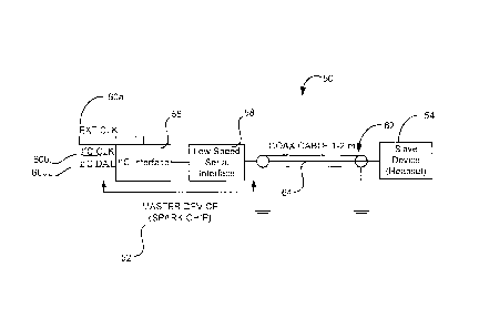
Turning to Figure 3, a schematic diagram of a single wire bus system is shown.
The single wire bus system 50 includes a master device 52, such as a portable
electronic
device or a headset interface chip within a portable electronic device, and a
slave device
54, such as a headset. Although only one slave device shown, it will be
understood that
multiple slave devices may be connected to the master device 52. The master
device 52 or
slave device 54 may include an Inter-Integrated Circuit (I2C) interface 56
which is
connected to a baseband processor or other mobile processing unit. The master
or slave
device may also include an I2C interface for digital audio data. Inputs, or
input signals, 60
3
CA 02759946 2011-11-29
to the I2C interface 56 and a serial interface 58 may include, but are not
limited to, an
external clock 60a (EXT CLK), an I2C clock 60b (I2C CLK) and an I2C data
signal 60c
(I2C DAT). An output of the low speed serial interface 58 is connected to the
slave device
54 via a cable 62, such as a co-axial cable. As described above, one of the
wires 64 within
the cable 62 is used for communication between the slave device 54 and the
master device
52 and can be seen as the single wire bus.
One advantage of the current disclosure is that with this architecture, a
single wire
bus may combine multiple functions, including, but not limited to, the
transmission of
both clock and data in a single bus cycle. In operation, the I2C interface 56
retrieves and
sends data to the slave device 54 over the designated single wire 64, or line.
In other
embodiments, the single wire bus may be controlled via a connection to the
baseband
processor or other processing unit. The master device 52 generates framing
information in
order to allow the slave device 54, or multiple slave devices, to be
synchronized to the
single wire, or communication, bus 64. In one embodiment, the frame length is
determined by an 8-bit register that provides a separation distance between
the start of
each block of command data. In another embodiment, the unit of measure is a
nibble
which equals four (4) bits. The minimum frame length is determined by the
command
pattern and in one embodiment may be 48 bits with a default sync separation
value of 28
nibbles thereby resulting in a frame length of 384 bits.
In operation, a synchronization signal (sync), control signals of information,
data, a
clock signal and power is transmitted between the master device 52 and the
slave device
54 over the single wire bus 64. The clock signal can be used as sampling clock
for
internal circuits such as sigma-delta converters or for continuous operation
of a complex
logic circuit.
One advantage of the system is that the size of components for use in
communication via the single wire bus may be decreased. For example, if
implemented in
the portable electronic device of Figure 2, the single wire bus of the present
disclosure
allows for the clock signal and the data to be transmitted over a single wire
which reduces
the number of pins required to be occupied in the chip 32 thereby allowing the
other pin
ports 42 to be used for other functionality or to reduce the total pin-count,
silicon area or
cost of the chip.
In one embodiment, the bus is implemented using a low-high-float cyclic
pattern
but may alternatively be implemented as a high-low-float pattern. The float
period is used
4
CA 02759946 2011-11-29
for signalling, while the low-high (or high-low) period is used to transfer
power and for
clock synchronization. As the period during which the bus floats is very
short, it may be
kept stable due to parasitic capacitances or may be kept stable for longer
periods of time
by including a bus holder within the system. Therefore, the charge and
therefore the
voltage on the bus may be considered stable, if unloaded statically or loaded
by a high
impedance. In a given implementation, either a low-to-high or a high-to-low
edge
triggered phase lock loop (PLL) may be used for synchronization, though it is
possible to
synchronize an external device to the bus using controlled delays with a delay
locked loop
(DLL) or a fixed delay value circuit. The delay unit may comprise two
capacitors that are
being alternately charged by a fixed current and then using the charging
voltage on the
capacitors to determine the points where the bus should be activated and
sampled. These
two capacitors may be charged from one fixed clock edge to the second fixed
clock edge
and discharged before starting this cycle.
In one embodiment, a minimum bus capacitance and minimum clock frequency
should be observed (i.e. be sufficiently high), so that the reading of the
status of the bus
during the floating, or tri-state, period is uniquely defined. If the bus
system is
implemented on a printed circuit board, a small capacitor may be used to
provide a
significantly large charge to protect against data errors. In this case, a
small but finite bus
capacitance is required or alternatively implemented using the bus holder
(e.g. using two
inverters coupled back-to-back) to maintain a stable bus value. This method
may be
chosen for low frequency operation of the bus, where small leakage currents
may slowly
discharge any charges left on the bus, but a bus holder will keep the value
stable. The bus
holder will normally be implemented in the master device to limit the power
efficiency
loss associated with its operation but can also be implemented in slave
devices for data
integrity purposes.
Furthermore, if a slave device or the master device wants to signal a logic
zero,
that device will leave the bus in the same state as before i.e. floating and
with the same
value on the bus as will be discussed below. In one advantage of the
disclosure, the bus
structure reduces or avoids bus contention, or congestion, when multiple
devices try to
signal, or communicate over the bus, at the same time, since once the bus has
been
discharged, the discharge of the bus by subsequent devices is not detected and
bus
collision is not possible.
. = CA 02759946 2014-01-29.
=
Turning to Figure 4a, a timing diagram of communication, or a communication
protocol, between a master device and a slave device is shown. In the current
figure, a
single clock cycle is shown. At the beginning of the clock cycle, the signal
on the bus is
low and then is pulled high by the master device. At some point during the
time cycle,
this signal is pulled down, or discharged, to prepare for the next clock
cycle. During
periods, or clock cycles, where transfer of information is not required, it is
possible to let
the bus go idle by setting the clock signal constant high. Alternatively, the
signal on the
bus can be left low and then be pulled high in order to signal that a slave
device would like
to communicate with the master device or to transmit data over the bus. During
one clock
cycle, one bit is transmitted between the master device and the slave device.
Between the time when the clock signal is pulled high and the end of the clock
cycle, there is a tri-state area where the signal can either be pulled down by
the master
device or the slave device. In one embodiment, if the clock signal is pulled
down by the
master device, the master signal a logic "1" and the next clock cycle is
started. If the
clock signal is pulled down by the slave device, it is the slave device that
signals a logic
"1". This is described in more detail below with a specific example of
communication
over the bus.
In one example mode of operation, over 16 clock cycles, the master device
transmits information, such as a sync word over the bus. As schematically
shown in
Figure 4b, an example timing diagram of the master device transmitting a sync
word of
111111111101100 over the single wire is shown. Therefore, for any slave
devices which
are connected to the bus, they may lock onto the bus via the sync word so that
their
internal state machines and thereby timing are synchronized with the master
device.
Turning to Figure 5, a schematic diagram of a timing diagram whereby a slave
device writes"0110" is shown using the communication protocol of Figure 4a. In
general,
the bus is time-multiplexed in four time intervals. In operation, the bus is
active low (from
the previous clock cycle) for the first quarter of the clock period and then
is driven active
high by the master device, normally for the second quarter of the clock
period. This low-
high transition may be used as a continuous sampling clock signal. The bus is
then left in
a floating state for the remainder of the clock period unless a slave device
54 or the master
device 52 pulls the bus low to signal a "1". This typically occurs in the
second half of the
clock period so that the bus is fully settled by the end of the clock period.
The bus value is
sampled near the end of the clock period just before or at the same time the
master begins
6
CA 02759946 2014-01-29
=
to drive the bus low to start the next clock cycle. In one embodiment, the
first half of the
clock cycle may be used for the clock signal while the second half of the
clock cycle may
be used for the data transmission. However, other divisions of the clock cycle
are
contemplated such as 67% clock and then 33% for the data transmission.
In the example of Figure 5, the bus is initially active low at the beginning
of the
clock cycle. After a particular period of time, the bus is driven active high
by the master
device. As the slave device wishes to transmit a "0" seen as active high, the
slave device
does not do anything with the bus. The value of "0" is then read by the master
device and
the slave device before the master device drives the bus to an active low
prior to the next
clock cycle. During the second clock cycle, the master device drives the bus
to an active
high after a particular period of time. As the slave device wishes to transmit
a "1", the
slave device pulls or drives the bus to an active low where the value is then
read by the
master device and the slave device. As the bus is active low, the master
device does not
have to drive the bus active low, although it may perform that function as
shown in Figure
5. In the third clock cycle, after a particular period of time, the master
device drives the
bus to an active high. As the slave device wishes to transmit a "1", the slave
device pulls
or drives the bus to an active low where the value is then read by the master
device and the
slave device. At the start of the fourth clock cycle, the bus is active low
and after a
particular period of time is driven bus active high by the master device. As
the slave
device wishes to transmit a "0", there is no activity on the bus until after
the value has
been read and then the master device drives the bus active low in preparation
for the next
clock cycle.
The timing of when the bus is pulled low by the master device is after a
particular
period of time so that incorrect data is not sampled by the master or the
slave devices. The
slave device requires a floating output when the master device pulls the bus
high.
When the master device or the slave device enters the tri-state, this is
represented
by dashed lines between the top (high) and bottom (low) levels even though the
actual
voltage will be determined by the previous values written to the bus. In the
preferred
embodiment, the output voltage during the tri-state is determined by the
charge and
parasitic load impedance of the bus, or line.
In some scenarios, it may be necessary for the slave device to activate the
data line
(or bus). In order to activate the bus at a particular time interval, a local
clock can be
implemented via a phase lock loop (PLL), a dynamic lock loop (DLL) or a delay
circuit.
7
CA 02759946 2011-11-29
Since the master device is used to control the timing, there is no requirement
for analog
controlled delays on the master device.
After indicating that there the slave device wishes to communicate with the
master
device by actively pulling the signal down during a ping operation, data can
then be
transmitted between the slave device and the master device via a read or a
write operation.
The master can also initiate a read or write operation on its own. In order to
initiate the
communication, the master device and the slave device need to be synchronized.
In the
current embodiment, the control words, such as the sync word, the X word and
the Y word
are transmitted in a single grouping of 16 bits, or clock cycles.
As schematically shown in Figure 4c, a single time frame is shown.
Communication between the master device and a slave device occurs during a
time frame.
The transmission of a sync word by the master device allows one of the slave
devices
which is physically connected to the bus to be locked on for communication
with the
master device. Depending on the application, or use of the bus, either for
audio
transmission or for the transmission of bitstreams, different sync words may
be used. The
selection of the fixed portion of the sync word is such that it is a pattern
of bits that does
not regularly occur in an audio or bitstream so that its use as a sync word is
not
compromised. As an example, the fixed portion for an audio sync word may be
0xB25
(hexadecimal) when the bus is used in audio transmission and the fixed portion
for a
bitstream sync word may be OxFFE when the bus is being used in a bitstream
transmission.
Turning to Figures 13a to 13e, examples of various frame structures are shown.
Figure 13a is a frame structure with a command separation of 0 bits. Figure
13b is a frame
structure with a command separation of 84 bits. Figure 13c is a frame
structure with a
command separation of 112 bits. Figure 13d is a frame structure having a bit
interleaved
processing type with 3 bitstreams and Figure 13e is a frame structure having a
bit
interleaved processing type with 7 bitstreams.
In one example, the frame length is 384 bits long, however it will be
appreciated
that shorter or longer lengths are contemplated and may be associated with the
clock
frequencies at which the bus is operating or where the oversample ratio is
better suited for
other numbers than 64. For instance, it may be advantageous to use oversample
ratios of
50 or 100 when using a clock frequency of 19.2 MHz (commonly used in mobile
systems)
8
CA 02759946 2011-11-29
since this will allow support for a 48 kHz sampling rate without requiring
sample rate
conversion methods. In this case, a frame length of 400 may be used.
Control of the master device can be via the I2C interface, through another
control
interface or as part of a connection to a digital signal processor (DSP) or
microprocessor
unit, which will provide the necessary information to have the master device
ping or
perform a read or write operation. The master device also generates the
framing
information necessary in order to synchronize external devices to the bus.
After going out
of the idle operation, the interface should enter a ping operation since the
slave devices are
not locked to the bus after power has been down.
Between the transmission of the sync word and an X word (operation of which
will
be described in more detail below), random data or information may be
transmitted over
the bus which can be picked up by the slave devices or the master device. This
information includes, but is not limited to, bit streams or audio data.
Transmission of the
X word allows the master and slave devices to determine if any specific
function is to be
executed or to determine if any interrupts have been set. After transmission
of the X word
(assuming that there were no interrupts set), further data, such as audio
data, may be
transmitted over the bus. A Y word is then transmitted which further outlines
the
functions and also other information between the master device and the slave
devices to
determine if there are any errors on the bus or with the slave devices.
Ping and read or write commands may not occur in the same frame since each
frame is defined by three different functions. All frames commence with the
sync word,
followed by the X-word and then the Y-word. Between the command words, there
may be
empty space allocated for data transmission depending on the use scenario. The
length of
the empty space is defined by the sync separation register.
The transmission of the X or Y word may result in a ping operation, a command
data read or a command data write being issued. In one embodiment, if the
command is a
command data read, a 16 bit word is read from the slave device which is
aligned with the
master device and if the command is a command data write, a 16 bit word is
written to the
slave device which is aligned with the master device.
In operation of one embodiment, when a ping command is issued, the X and Y
command words (or registers), as shown in Figures 10a and 10b, respectively,
are
transferred to the single bus. If the slave device wishes to request an
interrupt, a "1" or
high logic level is written to the X15 bit in order to indicate the interrupt.
This may be
9
CA 02759946 2011-11-29
used to delay a read or write operation and is written before the master
device is able to
signal its current operation.
If the X14 register is equal to "1", a "ping" operation is initiated. This bit
is
written by the master. A ping operation occurs when no read or write command
is being
performed or if the value of X15=1 and the value of X15 DELAY B5 (IRQ mask)=1,
i.e.
if the interrupt mask is disabled or if a pending input/output operation has
been delayed
due to a recognized slave interrupt.
X word bits, X13-X12, are equal to "11" during a ping operation and any other
value of this field is left for future expansion. If the value read is not
"11", the contents of
the command frame (X and Y values) should be ignored. The ST13:STO bits shall
be set
by any external device to indicate status and are located in the XO-11 and YO-
15 bits. Each
device can respond with three different status levels or choose not to respond
at all. These
bits may generate an interrupt based on the setting of the interrupt mask
register. This
ping command is active at all times, unless the master (headset chip) has
activated a read
or write command and is currently processing it.
The ping command is a general command to determine the status of the devices
which are connected to the bus.
In order to communicate with the slave device, the master device transmits a
sync,
or synchronization, word that the slave device (or devices) may use to
synchronize their
internal timing, or clock, with the master device. In one embodiment, the sync
word
comprises a 12 bit constant and a 4 bit pseudorandom value, or register value.
The
constant portion of the word is used by the slave device to reduce the
likelihood, avoid or
eliminate false sync words or positions within a frame. For instance, data may
be
transmitted over the single wire bus by other slave devices which appear to be
the sync
word but since it is not transmitted by the master device, they are, in fact,
false sync
words, and should be ignored by non connected slave devices. The pseudorandom
register
is also used to verify the start position of the frame. This allows a quicker
time-to-lock
and reduces the likelihood that slave devices lock on to false single words
created by
random data on the bus. Typically, a slave device would verify the pseudo-
random pattern
multiple times before locking on to the bus.
Once a slave is connected to the bus, various data, such as audio data or
bitstream
transmission may be transmitted over the bus. The time period between the
transmission
CA 02759946 2011-11-29
of the sync word and the X word is set to a particular value and in one
embodiment is a
multiple of 4 bits, or clock signals, up to a maximum of 4 * 255 or 1020 clock
signals.
When the X word is transmitted, each of the connected slave devices may
determine the type of operation, such as read or write, being performed by
reviewing the X
word. The master device can determine if any of the slave devices have
initiated an
interrupt by checking bit 15 of the X word. An interrupt may be signalled if
there is an
error or if one of the slave devices requires assistance or is not operating
in an expected
manner or has an important statue message to send.
The X word represents a control word in the time frame and determines if any
slave device is waiting for an interrupt request. Bit 15 of the X word, or
X15, also
determines the action for read or write applications and does not affect the
way a ping
operation is progressing. This bit may be masked so that it does not block bus
traffic.
If the X15 bit has not been set, the master device and the locked on slave
devices
read the information from the X word to determine if there is any activity on
the bus or
any activity to be performed over the bus between the master device and a
specific slave
device.
If the X15 bit has been set and the interrupt detected and acknowledged, a
signal,
such as a status or ping request, a read command or a write command, is
transmitted by the
master device based on data received from an I2C transfer. The master device
then delays
the current operation in order to determine which slave device signalled the
interrupt and
to determine the issue that needs to be resolved. This information can be
found in the Y
word which is transmitted after a specific time period (which is identical to
the time period
between the sync word and the X word).
When a data read command is issued, the X and Y command words (or registers)
as shown in Figures lla and 1 lb respectively, are transferred to the single
bus.
If a slave device needs to request an interrupt of the communications, the
read
operation may be delayed by activating the X15 bit, or by setting the
interrupt request. If
no slave device has activated this bit (`1' means activate) or if the IRQ mask
is disabled,
the data read command will proceed. If the delay is activated, the slave
device which
requested the interrupt has a status level equal to "10" or "11" and the
corresponding IRQ
mask bit is set. This slave device should copy the contents of the most
significant bit of its
status register onto the bus during the delay.
11
CA 02759946 2011-11-29
If there is no interrupt, the X14 bit is set to a "0" which signifies a read
or write
register operation and the setting of the X13 bit to 1 signifies a read
operation.
In order to confirm if a message has been correctly received, the acknowledge
message bit is written by a slave device. The value of this bit is set to
logic high, when no
error has been detected on the bus during the delivery or communication of
command
words in this frame, such that the slave device is present and has the same
address that the
master device has written to. The master device recognizes which slave device
it is in
communication with and therefore the address of the slave device may be
confirmed on a
regular basis to reduce the likelihood or errors, If an error has occurred (a
bit read from
bus is different from what was expected), the master device reports a bus
error. This
protects against any device unintentionally writing to the bus and against bus
errors. A
slave device should signal logic zero, if the data transmission has been
corrupted during a
read application. Further, the slave device sets the acknowledge bit, since it
is the only
device, that knows if an error has occurred, e.g. that the parity bit is wrong
or a bus error
has occurred. If no slave device is connected to the bus, a logic zero will be
returned from
the bus, by nature of the bus signalling scheme indicating a problem to the
master.
When a data write command is issued, the X and Y command words (or registers)
as shown in Figures 12a and 12b respectively, are transferred to the single
bus.
The purpose of the X15 bit is to delay a write operation, if a slave device
has an
important status message to send or has transmitted an interrupt request. This
is done by
activating the X15 bit. If no slave device has activated this bit (`1' means
activate) or if the
IRQ mask is disabled, the data write command may proceed. If a delay is
activated, the
delay is treated in a similar manner as disclosed above with respect to the
data read
command.
The start of a data write command operation is signalled by register bits
X14:X13="00". Y14 is defined such that a slave device may not force a data
read or write
command with control being provided by the master device. Furthermore, a slave
device
may not force a data write command when a data read command has been chosen.
However, a slave device can (by error or deliberately) change a read or write
operation to
a ping or a write command to a read command. This should be considered a bus
conflict.
If the X14 bit is set to a "0", no slave device is allowed to answer with IRQ
information
(i.e. this signifies a read/write register operation).
12
CA 02759946 2011-11-29
The slave device should acknowledge to the master device, that it has read and
accepted the message at the end of a data write command. The slave device
addressed by
the master sets this bit to logic one to indicate that there is no parity
error and it has
accepted the data. The slave device that responds must be locked on bus and
have same
address as the device the master is intending to write to. If a bus error has
occurred and is
detected by the master device, the master device should set the bus error bit
active and try
the data write command again.
When data is written to or from the slave device, eleven bits are used for
addressing while four bits are used to select the specific slave device and
seven address
bits are reserved to select which register within the slave device that is
being written, other
address and register spaces could also be used. The last two bits of the X
word are used
for register reading or writing commands.
The last control word (Y) is used to communicate data between the master
device
and the slave device, or devices. In one embodiment, this data may be data
that is to be
written to or read from a slave device register (when no interrupt has been
signalled). In
another embodiment, this data may be the polling of an interrupt status from a
slave device
to determine which slave device has set the interrupt request. The length of
the data is 16
bits which includes the last two bits of the X register. The last two bits of
the Y registers
are used for data integrity. Other data lengths may be used in other
implementations.
Therefore, if there was no interrupt set in the X15 bit, the Y word, or Y
control
word, may be polled to determine information, as listed above. If an interrupt
was
signalled in the X15 bit and the associated interrupt mask bit was enabled,
the master
device polls the slave device using a ping operation. Here, the X and Y words
are used to
determine which slave device signalled the interrupt. This is disclosed in
more detail
below with respect to the status levels of the slave devices. In the X and Y
words, certain
registers are designated for slave devices so that the master device can
quickly determine
the status level for a specific slave device. A schematic diagram of part of a
Y word is
shown in Figure 4d.
In order to signify that it wishes to communicate with the master device, as
disclosed above, the slave device can generate an interrupt, typically during
a ping
operation or activate X15 of the X word during any time frame. The slave
device can then
send an interrupt request (IRQ) to the master device during a ping operation
using slave
address zero since this address is allocated to non-assigned slave devices, or
baseband
13
I = CA 02759946 2014-01-29,
=
=
chip, via the single wire bus such as schematically shown in Figure 4d which
indicates the
status for the five slave devices connected to single wire bus. Although only
five slaves
are shown, any number of slaves may be connected to the bus..
The slave device may have four status levels via their two bits, namely "00",
"01",
"10" and "11". "00" typically represents that the slave device is not locked
on to the single
wire bus. "01" signals that the slave device has locked onto the bus and this
status may be
used to detect when, and if, the slave device has disconnected from the bus.
"10" signals
that the slave is locked onto the bus but wishes to get the attention of the
master device.
This slave status level will also delay a read or write operation if the IRQ
mask is active.
A "11" signals that the slave device has an emergency situation that needs to
be handled
immediately, such as, but not limited to, the temperature of the device is too
hot or there is
a critical undervoltage or overvoltage. This status level will delay a read or
write
operation, if the IRQ mask is active. Therefore when an interrupt is sensed,
the master
device polls the Y word to determine which slave devices require attention. In
the
example of Figure 4d, slave device 4 has a status level of "10" while slave
device 5 has a
status level of "11".
With respect to the ping operation, the values stored in the X1 I :XO & Y15:Y0
registers of the X and Y words updates the status register. The highest value
which is read
from a slave device is compared to the slave status register and the register
value is
updated if the value being read is higher than the current slave status
register value. In this
manner, the slave device requiring the most attention receives immediate
attention. When
the slave status register is read, its value is not cleared by overwriting
during a subsequent
ping operation. In other words, the status level of slave 5 will be determined
to require
immediate attention and its status level written to the status register. After
the ping
operation has been completed then the status slave register will be updated to
reflect the
updated register values.
Figures 4e to 4g show other clock signal options or other communication
protocols
or how to transmit logic highs and logic lows over the bus. In Figure 4e, the
clock signal
is initially pulled high (as in Figure 4a), however, this represents a logic
"1" signal such
that if either the master device or one of the slave devices wishes to
transmit a logic "0"
during the data portion of the clock cycle, the clock cycle must be pulled
down. In order
to transmit a logic "1" signal, the clock signal is left unchanged until
closer to the end of
the clock cycle (after the bus has been sampled).
14
CA 02759946 2011-11-29
In Figure 41', the clock signal is initially pulled low in order to indicate
the leading
edge of the clock signal. In this embodiment, in order for one of the master
device or one
of the slave devices to signal a logic "1" during the data portion of the
clock cycle, the
device is required to pull the clock signal high. If the master device or one
of the slave
devices wishes to transmit a logic "0", the clock signal is left untouched
until closer to the
end of the clock cycle (after the bus has been sampled).
In Figure 4g, the clock signal is initially pulled low in order to indicate
the leading
edge of the clock signal. In this embodiment, in order for one of the master
device or one
of the slave devices to signal a logic "0" during the data portion of the
clock cycle, the
device is required to pull the clock signal high. If the master device or one
of the slave
devices wishes to transmit a logic "1", the clock signal is left untouched
until closer to the
end of the clock cycle (after the bus has been sampled).
When slave devices lock onto the bus, the master device communicates with the
slave devices to retrieve their address. Initially, all slave devices start
off with an address
of zero and therefore, if there are three (3) slave devices attempting to lock
on to the bus,
each one is initially assigned the value of zero. However, as will be
understood, each of
these devices will have an internal identification, or a unique name
associated with the
slave device. Typically, the unique name of the slave devices is 32 bits or
more.
After the issuance of a PING command by the master device, if a slave device
wishes to lock onto the bus, the end of the X word is populated with the
entries 01
(indicating the presence of at least one slave device wishing to lock onto the
bus). Once
this is recognized by the master device, the master device performs a read of
the name of
the device or devices which have attempted to connect to the bus in order to
assign an
address to the connected slave device. As will be understood, if no slave
devices are
currently connected to the bus, the master device continues to complete the
frame and then
issues a further ping in the next frame cycle.
If at least one slave device is present, the master device reads the first bit
of the
unique name of all the slave devices looking to be assigned a unique address.
The first bit
of the unique name for each slave device is then reviewed. If they are all the
same i.e. all
"1" or all "0", the master device proceeds to, or polls, the next bit of the
slave device
names. If there is a combination of "0" and "1"s, then the master device
continues only
with the unique names which have a "1" as it will determine the bus value due
to the
dynamic nature of the bus. Thereby the master device will review the unique
names in an
CA 02759946 2011-11-29
"alphabetical order", where the slave device with the higher numerical name
value is
assigned a slave address before a slave device with a lower numerical name
value. The
numerical value of the slave device name is determined from a sorting based on
a binary
search, with the values being read as binary numbers. If there is only a
single "1" value,
then the master device assigns the slave device associated with this unique
name as the
first device and assigns it a unique slave value 1-13 and then proceeds to
return to bus
communication where it will encounter another Olin the X word during the
subsequent
frame and therefore assigns a slave device address that is different from the
first slave
device to the next slave device in a similar manner. The determination of
which slave
device is to be assigned a slave address 1-13 continues until there are no
more unassigned
slave devices attached to the bus. As each slave device has a unique name,
there will not
be any situation where the master device does not know which slave device to
associate
with the current device address. In subsequent read and writes to slaves
devices, the
assigned slave addresses 1-13 will be used to identify these devices. If a
slave device
enters a hardware error condition and is reset, the slave address is set to
the default value
of zero.
In an alternative embodiment, the control words can be sent bit by bit in
order to
reduce the latency that is experienced. A schematic of how the sync word may
be
transmitted is shown in Figure 9. In this example, only the first four letters
of the sync
word are shown. In order for a slave device to lock on to the bus, it checks
every Nth bit
for the sync word in this mode. In the figure, every 4th bit is used. The
other control
words, X and Y, may be transmitted in a similar manner. By interlacing the
sync, X and Y
words with audio data content, it is possible to decrease the latency
experienced for the
data words, since the control words are limited to a delay of a single bit. In
this mode, the
slave device needs to search for the synchronization symbols with some spacing
between
these. In order to reduce the complexity of the search engine of the slave
device, a limited
number of variable spacing would typically be used, e.g. a spacing of 4 or 8
bits between
each synchronization symbol. In order to reduce the search time, the control
symbols
would typically be repeated without any extra spacing in between. This would
allow for
the transmission of three and seven bitstreams simultaneously with control,
when using
these two selected spacings between the control bits.
As can be seen, data may be transmitted over the audio or data channels
(listed as
1, 2 and 3) between sync word transmissions. As will be understood, any number
of audio
16
CA 02759946 2011-11-29
data channels may be used, up to a limit of 4 * 255 or 1020 channels between
the control
words.
In the following Figures, schematics of various registers for use within the
slave or
master devices for communicating over the bus are shown.
Turning to Figure 8, a schematic diagram of a status register is shown. In
operation, the status register provides status information from the bus and
control IRQs
and is controlled by read and write operations by the master or slave devices.
The status
register includes 8 bits which are designated BO to B7. As will be understood,
the default
value of the status register after it is reset is "00000000". This assists in
controlling the
data communication between the master and the slave device.
Each of the bits within the status register can be read and used by the master
controller. Bit BO represents the FRAME DONE bit, Bit B1 represents the RD
bit, Bit B2
represents the WR bit, Bit B3 represents the ATTACHMENT bit, Bit B4 represents
the
STATUSO bit, Bit B5 represents the STATUS1 bit, Bit B6 represents the 10 ERROR
bit,
and Bit B7 represents the BUS ERROR bit.
More specifically, the bus error bit (B7) signifies an illegal bus operation
has
occurred and is active high. This condition can be detected if the value on
the bus is
different than it should be during a master bus write operation (e.g. a slave
is conflicting
with the sync pattern). Once an illegal bus operation has been detected, it
will remain set
until this register has been read. An interrupt will be generated if illegal
bus operation is
observed and the corresponding IRQ mask bit is enabled (i.e. set high).
The 10 error bit (B6) signifies an error during a read/write operation. It
will be set
if a slave device does not acknowledge a read/write command (i.e. the
acknowledge bit YO
in a read/write command is not activated/"1"). It is reset upon reading the
status word.
This bit is calculated as the combination of the WR and RD bit, see
description of these.
The Statusl and Status() bits give the highest status level read from any
device
attached to the bus. If any slave has a status level higher than indicated by
these two bits,
they will be updated to this new value during the next ping operation. The
bits will
continue to be updated to any higher status level read, until this register is
read. A read of
the status register will not clear this field but it will be updated to the
highest status level
read during the next ping operation. It is updated during every ping operation
and power-
on reset and thus always valid. As an example, the register value is "00"
after reset and
"01" after a device has been attached to the bus. Then assume a device needs
urgent
17
CA 02759946 2011-11-29
attention and signal "11" during a ping frame. The status register is then
updated to this
value. After reading the status register, the value is still "11". Assume
during the next
frame that the highest device level is now "10". At the end of the ping
operation, the status
register will be updated to this new value ("10"). This is done so that errors
are first
cleared when the slave device confirms this. If the interrupt mask has been
enabled and an
interrupt has been generated as a result of a slave requesting attention, the
IRQ line will be
cleared upon reading the status register. A new interrupt will be generated
during next
ping operation, if the slave still requests attention and the interrupt mask
bit is set. During
normal operation, a read from this field will return "01". I.e. one or more
devices are
attached to bus and there is no requirement for special service. This field
can both be used
to determine if any devices are attached to the bus or distinguish between
devices
requiring attention with low (status level "10") or high priority (status
level "11"). If no
devices are attached to the bus, it will return "00".
The Attachment bit (B3) is active high and will indicate if a device has
disconnected or connected to the bus since last ping operation. The value can
be found by
comparing the device status from X and Y words during a ping operation to
previous
values. If the status for any device has changed from {"01","10","11"} to "00"
(i.e. a
device has disconnected from the bus) the signal will go high. If the status
has changed
from "00" to {"01","10","11"} (i.e. a device has attached to the bus) the
signal will go
high. The attachment bit will stay high ("1") after being set until the status
register has
been read at which moment it is cleared. In any other case, the signal will
stay low. This
will indicate a change in attachment status for any device since last ping
operation. A
comparison is being made during every ping operation. By enabling the
corresponding
IRQ mask bit, this can result in an IRQ (pulling external SPARK IRQ line low)
being
generated as a result of a device is being attached or detached from the bus.
The default
value of this bit after reset is "0".
The WR Bit (B2) signifies a pending write operation and is active high. A
register
write operation will start by the I2C bus first writing to the data register
and then to the
address register. After the most significant word of the address register has
been updated,
the ACT WR bit will go high and an attempt of performing a write register
operation will
start in the next frame. Unless delayed by a device interrupt, the writing
will proceed
otherwise it will be delayed to the next frame and again attempted. After the
write
operation is complete, this bit will be reset again immediately after the last
bit of the Y
18
CA 02759946 2011-11-29
word. If the slave does not acknowledge the write operation the ERR_WR bit
will be set,
but the ACT WR will still go low. When the ACT WR bit is high, a new
read/write
operation should not be initiated until it has returned to low.
The RD bit (B1) signifies a pending read operation and is active high. A
register
read operation will start by the I2C bus writing to the address register.
After the most
significant word of the address register has been updated, the ACT RD bit will
go high
and an attempt of performing a read register operation will start in next
frame. Unless
delayed by a device interrupt, the read will proceed otherwise it will be
delayed to next
frame and again attempted. After the read operation is complete, this bit will
be reset again
immediately after the last bit of the Y word. If the slave does not
acknowledge the read
operation the ERR_RD bit will be set, but the ACT_RD will still go low. When
the
ACT RD bit is high, a new read/write operation should not be initiated until
it has
returned to low.
The Frame Done bit (BO) signifies a frame has been completed and is active
high.
It is set at the last bit of a frame. This may be used to synchronize
operations with the
basic timing of the bus. This bit is still valid when a device is being
charged and no
communication is active, i.e. the frame counter is always running internally.
It will
continue to be set until the status register has been read. It can be used to
tell if a ping
operation has been completed or for basic timing, e.g. to count a certain
number of frames
before starting communication to ensure all devices have been charged. When
the
corresponding IRQ mask bit is enabled, an interrupt will be generated at the
end of every
frame.
Turning to Figure 7, a schematic diagram of an IRQ Mask register is shown. In
operation, the Mask register provides information relating to any errors or
events which
may have arisen during operation of the bus system. The Mask register includes
8 bits
which are designated BO to B7.
Each of the bits within the status register are read by or written to by the
master or
slave devices. Bit BO represents the FRAME DONE bit, Bit B1 represents the RD
bit, Bit
B2 represents the WR bit, Bit B3 represents the ATTACHMENT bit, Bit B4
represents the
ATTENTION bit, Bit B5 represents the X1 5 DELAY bit, Bit B6 represents the TO
ERROR bit, and Bit B7 represents the BUS ERROR bit.
More specifically, the Bus Error Bit (B7) is used to enable or disable I2C
interrupts. When set to high, it will enable an interrupt based on an active
bus error bit in
19
CA 02759946 2011-11-29
the status register. The interrupt itself is signalled by a separate active
low level output line
and cleared when reading the status register.
The 10 Error Bit (B6) is used to enable or disable I2C interrupts. When set to
high,
it will enable an interrupt based on an active 10 error bit in the status
register (i.e. the
acknowledge bit YO in a read/write command is not set). The interrupt is
signalled by an
active low level output line and cleared when reading the status register.
The X15 DELAY bit (B5) is used to enable or disable the delay of read and
write
operations when a slave device requests attention. When set to high, it will
enable an X15
delay operation based on the value read from the bus during the X15 time slot.
A slave
will activate the X15 bit to signal a need for attention when the slave device
status is "10"
or "11" i.e. slave devices should copy the MSB of their status register during
the X15 time
slot. If the current operation is a read or write operation, it will be
delayed until next frame
and be replaced by a ping operation. At the start of the next frame, a read or
write
operation will be reattempted. A ping operation will proceed unaltered
irrespectively of
the value of the X15 bit. By enabling the X15 DELAY bit we will have a
guaranteed
latency of at most one frame if any device should require attention. Data
traffic outside the
command words can still continue while reading device status. If the IRQ mask
X15 bit is
inactive (low) any read or write transaction will proceed irrespectively of
the value of the
X15 bit. The master should clear this bit in software when an IRQ occurs to
avoid
blocking the reading or writing of slave registers.
The ATTENTION bit (B4) is used to enable or disable I2C interrupts based on a
slave device attention request during a ping operation. When set to high, it
will enable an
interrupt based on a slave status level of "10" or "11". In other words, when
enabling this
IRQ mask bit, the master will generate an interrupt whenever a slave device
requests for
attention. The interrupt is signalled by an active low level output line and
cleared when
reading the status register. If the slave device is still requesting for
attention and the
attention bit continues to be enabled during next ping operation, a new
interrupt will be
generated. The master should clear this bit in software when an IRQ occurs to
avoid
multiple interrupts being generated.
The ATTACHMENT bit (B3) is used to enable or disable I2C interrupts. When set
to high, it will enable an interrupt based on a change in the status register.
The interrupt is
signalled by an active low level output line. The interrupt is generated
whenever the
STA1:STA0 field changes value due to attachment or removal of a slave device
to the bus.
CA 02759946 2011-11-29
This can happen, if a slave device changes value and this value has been read
by a PING
operation. If a device status change and the IRQ mask device status bit are
enabled, an
interrupt is generated. The interrupt is cleared when reading the status
register. If the status
value read indicated the need for master intervention, the normal operation
for a master
controller would be to read back the device status values from the slave
status register to
find the source of the interrupt. After this has been completed, any necessary
action can be
carried out by writing register control commands to the slave device in
question.
The WR Bit (B2) is used to enable or disable I2C interrupts after write is
complete.
When set to high, it will enable an interrupt based on the completion of an
active write
operation. The interrupt is signalled by an active low level output line. The
interrupt is
cleared when reading the status register. The source of the interrupt may be
detected by
activating a separate bit or by setting both the ACT_RD and ACT_WR register
bits active
at the same time to indicate the completion of an 10 operation.
The RD Bit (B1) is used to enable or disable I2C interrupts after read is
complete.
When set to high, it will enable an interrupt based on the completion of an
active read
operation. The interrupt is signalled by an active low level output line. The
interrupt is
cleared when reading the status register.
Finally, the FRAME DONE bit (BO) is used to enable or disable I2C interrupts
based on the completion of a frame. When set to high, it will enable an
interrupt based on
the completion of the internal frame counter. The interrupt is signalled by an
active low
level output line and cleared upon reading the status register. The internal
frame counter in
the master should still be running during charge mode.
One advantage of the present disclosure is that the bus is robust against
multiple
sources signalling at the same time and does is an improvement over time-
constrained
implementation problems as when using open-collector and open-drain type,
where the
signalling speed is a compromise between power consumption and noise immunity.
The above-described embodiments are intended to be examples only. Those of
skill in the art can effect alterations, modifications and variations to the
particular
embodiments without departing from the scope of this application.
21