Note: Descriptions are shown in the official language in which they were submitted.
CA 02760255 2011-10-27
WO 2010/124965 PCT/EP2010/055169
-1-
ELECTRICAL CONNECTOR WITH IMPEDANCE CORRECTION ELEMENT AND
METHOD FOR THE MANUFACTURE THEREOF
The present invention relates to an electrical connector with an electrically
insulating contact
carrier and with at least one electrically conducting contact element which is
held in the contact
carrier. Furthermore, the present invention relates to a manufacturing method
for manufacturing
a connector of this type.
Signal lines generally transmit no direct current, but only pulsed current or
alternating current.
In order to prevent pulse reflections on signal lines, they must have above
all a uniform, i.e.
constant impedance. Reference is made to what is known as nominal impedance.
Accordingly,
for connecting lines, in particular in relation to high-speed data
transmission, care must be taken
to ensure that a constant impedance of this type is also adhered to in the
associated plug
connectors.
In principle, nominal impedance Zõ is a property of pairs of signal lines. The
nominal impedance
is approximately independent of the length of the line, as the direct current
resistance is
negligible in signal lines of this type compared to the pulse resistance.
In known plug connectors, changes in diameter are provided along the
electrical contact
elements in order to compensate for fluctuations in impedance along the pin
strip that are
produced by changes in the geometry of the pin strip. Furthermore, it is known
to bend the
contact pins, which each pertain to complementary pairs of signal conductors,
accordingly in
order to generate a compensation of impedance.
However, these known methods on the one hand increase the cost of manufacture
and on the
other hand have the drawback that an altered nominal impedance can be
implemented only by
changing the tool.
The object on which the present invention is based consists in disclosing an
electrical connector
with an electrically insulating contact carrier and with at least one
electrically conducting
contact element that can be manufactured economically and the impedance of
which is
particularly simple to set.
CA 02760255 2011-10-27
WO 2010/124965 PCT/EP2010/055169
-2-
This object is achieved by the subject matter of the independent claims.
Advantageous
developments of the electrical connector according to the invention are the
subject matter of the
independent claims.
In this regard, the present invention is based on the idea that an impedance
correction can be
implemented in a particularly simple manner in that an impedance correction
element is
arranged in the contact carrier for setting the impedance of the connector in
the region in which
the at least one contact element is arranged. A contact correction element of
this type on the one
hand can compensate for fluctuations in impedance along the pin strip that are
produced by a
change in the geometry of the pin strip and on the other hand can prevent
jumps in impedance at
the end of the pin strip.
According to a first advantageous embodiment of the present invention, an
electrically
conductive correction pin, which will be referred to hereinafter also as an
impedance correction
pin, can be used to compensate for impedance in a specific region of a contact
carrier which may
be a carrier both for sleeves and for pin contacts. If this impedance
correction pin is inserted into
the contact carrier parallel to the contacts having a defined geometry, depth
and length, it is
possible to generate an almost constant impedance course along the contact
carrier. Jumps in
impedance can thus be avoided and, in an advantageous manner, an impedance
correction pin of
this type allows the impedance to be purposefully set to so as to differ from
the nominal
impedance.
Alternatively or additionally to the impedance correction pin, an electrically
insulating
impedance compensation element can also be provided in the form of a
dielectric element. This
impedance compensation element is advantageous for preventing jumps in
impedance at the end
of the pin strip, in particular in the case of angled 90 downturns of the
contacts. In this case,
this additional element can either have the same dielectric constant as the
contact carrier or else,
as required, display a specific different dielectric constant.
In order to be able to adapt the impedance of the connector in a particularly
simple manner, the
contact carrier is constructed in such a way as to have a connection region
for connecting a first
external component and a contact region for contacting a second external
component, the
connection region and the contact region being joined together by a connecting
region.
According to the invention, a large number of contact elements are arranged in
the contact
carrier and the contact elements are symmetrically integrated in a cross
section of the connecting
region.
CA 02760255 2011-10-27
WO 2010/124965 PCT/EP2010/055169
-3-
According to an advantageous embodiment of the present invention, the contact
carrier has in
the connecting region a borehole which is arranged symmetrically in relation
to the contact
elements and is preferably arranged centrically equidistantly to the contacts.
This borehole is per
se a dielectric which is different from the plastics material of the connector
and can additionally
in accordance with the invention receive the electrically conductive impedance
correction pin.
The impedance of the electrical connector is set via the position of the
correction pin in the
borehole. Furthermore, the shape and length and also the material of the
correction pin influence
the impedance of the electrical connector.
In a particularly simple manner, an impedance correction pin of this type is
made of metal,
preferably as an extruded part or turned part.
The simplest cross-sectional geometry is a circular cross section, although
any other desired
cross sections can of course also be used for the impedance correction pin.
Thus, for example,
the cross section may also be square or rectangular or have a different shape,
depending on the
costs of the production method and the specific impedance requirements.
Furthermore,
depending on the requirements of the compensation of impedance, the impedance
correction pin
according to the invention can also have a diameter course which varies in the
longitudinal
direction, i.e. for example be waisted.
The use of the impedance correction pin eliminates the need to use contact
elements which have
a plurality of changes in cross section and would be required in order to
compensate for jumps
in impedance. A contact having a constant cross-sectional course can be
manufactured more
economically. Furthermore, a purposeful and locally precise compensation of
impedance or a
purposeful influencing of impedance can be achieved by purposefully placing
the impedance
correction pin in the longitudinal direction of the pin strip, and also by
selecting the length and
the cross section of the impedance correction pin. This is important above all
for use in high-
speed data (HSD) pin strips or similar applications for high-frequency signal
transmission.
According to an advantageous development of the present invention, the
impedance correction
element can have, alternatively or additionally to the impedance correction
pin, an electrically
insulating impedance compensation element. This dielectric element is used to
prevent jumps in
impedance at the end of the pin strip, in particular in the case of 90
contact downturns. As
mentioned hereinbefore, the electrically insulating impedance compensation
element can either
have the same dielectric constant as the contact carrier or else have a
different dielectric constant
selected for improving the signal quality.
CA 02760255 2011-10-27
WO 2010/124965 PCT/EP2010/055169
-4-
In an advantageous manner, the impedance compensation element is embodied in
such a way
that the contact elements are enclosed almost completely with plastics
material in order to set the
impedance to the impedance value of the pin strip even in the end region.
In order to improve understanding of the present invention, the invention will
be described in
greater detail based on the exemplary embodiments illustrated in the following
figures. In this
case, like parts are provided with like reference numerals and like component
designations.
Furthermore, a few features or combinations of features from the embodiments
shown and
described may represent solutions which are per se inventive or in accordance
with the
invention. In the drawings:
Fig. 1 is a perspective exploded illustration of an electrical connector with
an impedance
correction pin;
Fig. 2 is a cut-away illustration of the connector from Fig. 1;
Fig. 3 is a cut-away illustration of an electrical connector with an impedance
correction pin and
additional dielectric impedance compensation element; and
Fig. 4 is an unsymmetrical section through the embodiment of Fig. 3.
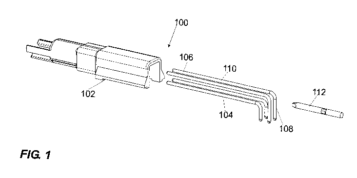
Fig. 1 is an exploded illustration of the electrical connector 100 according
to the invention in
accordance with a first advantageous embodiment.
The electrical connector 100 comprises a contact carrier 102 which is made of
a suitable
electrically insulating material. In the specific embodiment shown in this
figure, the plug
connector is an angled plug connector such as is used for a connection between
a printed circuit
board and a signal line, for example. The present plug connector 100 is
referred to as a four-pole
high-speed data (HSD) pin strip. A total of four contact elements are
provided, in this case
contact pins, which are denoted by reference numeral 104. However, the
principles according to
the invention may of course also be used for plug connectors with contact
sleeves as the contact
elements.
Each of the contact pins 104 has a connection region 106 for connecting a
first external
component, for example the plug connector of a signal cable, and a contact
region 108 for
contacting a second external component, for example a printed circuit board.
The connection
region 106 and the contact region 108 are joined together via a connecting
region 110, the
longitudinal axis of the contact region 108 being angled by 90 in relation to
the longitudinal
CA 02760255 2011-10-27
WO 2010/124965 PCT/EP2010/055169
-5-
axis of the connecting region and the connection region. The four contact pins
104 are arranged
symmetrically in cross section in the connecting region 110.
Changes in dimension in the geometry of the contact carrier and also
fluctuations in spacing and
geometry in the enclosing shielding (not shown in this figure) cause impedance
inhomogeneities
in the signal propagation direction that adversely influence the signal
quality. Furthermore, it
may be necessary to purposefully set the impedance so as to differ from the
nominal impedance.
As will become clear hereinafter with reference to the following figures,
according to the
invention, a metallic impedance correction pin 112 is therefore inserted into
the contact carrier
102 centrically to the four contact pins 104.
As is apparent from the illustration of Fig. 1, the adaptation of impedance
according to the
invention allows the cross sections of the contact pins 104 to remain constant
over the entire
length, allowing particularly economical manufacturability and mountability of
the contact pins
104 in the contact carrier 102 to be achieved.
The precise position of the electrically conducting impedance correction pin
112 in the contact
carrier 102 is made clear from the cut-away illustration of Fig. 2. As may be
seen from this
figure, the contact carrier 102 has a continuous borehole 114 arranged
centrally symmetrically in
relation to the contact pins 104 in the connecting region 110. The metallic
impedance correction
pin 112 is pressed into the borehole 114 to a defined depth to compensate for
impedance in a
specific region of the pin strip.
According to the invention, an almost constant impedance course along the
contact carrier can
be generated by the electrically conductive impedance correction pin 112 which
is inserted into
the contact carrier 102 parallel to the contact pins 104 having a defined
geometry, depth and
length. Jumps in impedance can thus be avoided and, in addition, the impedance
correction pin
also allows an impedance to the set that purposefully differs from the nominal
impedance.
According to the invention, to compensate for impedance in a specific region
of the contact
carrier 102, the metallic impedance correction pin 112 is inserted, parallel
to the connecting and
connection regions of the contact pins 104 with optimised spacing and at a
defined depth, length
and cross-sectional shape, into the contact carrier 102 in such a way that an
almost
homogeneous impedance course along the contact carrier is generated. In
addition to the
position in the borehole 114, the length as well as the cross-sectional shape
of the impedance
correction pin 112 can also vary as required. The impedance correction pin 112
is placed in the
CA 02760255 2011-10-27
WO 2010/124965 PCT/EP2010/055169
-6-
cross section-adapted borehole 114 in the contact carrier 102. There, it can
also be displaced as
required in the longitudinal direction in order to achieve a local
compensation of impedance or
purposeful influencing of impedance.
It goes without saying that the impedance correction pin 112 can also be fixed
within the contact
carrier at a predetermined position, for example by sheathing with plastics
material. In this way,
jumps in impedance can also be compensated for and a uniform impedance course
along the pin
strip can be achieved.
A further advantageous embodiment of the present invention will be described
in detail with
reference to Fig. 3 and 4. Alternatively or additionally to the metallic
impedance correction pin
112, an electrically insulating impedance compensation element 116 is provided
here. This
impedance compensation element 116 is slid onto the contact regions 108 of the
contact pins
104 in such a way that the contact pins 104 are enclosed almost completely
with plastics
material in order to set the impedance to the impedance value of the pin strip
in this region too.
This smooths the impedance course of the pin strip and the quality of the
signal to be transmitted
is improved by minimising the reflected signal components.
According to the invention, the impedance compensation element 116 can be made
of a material
either having the same dielectric constant as the contact carrier 102 or else
having a different
dielectric constant. In the embodiment shown in this figure, contact bushings
118 are provided
for the two longer contact pins, whereas the two shorter contact pins are only
partially
surrounded by the impedance compensation element.
The procedure in the mounting of the electrical connector according to the
invention will be
described hereinafter with reference to Fig. 1 to 4.
In this procedure, a basic element, the contact carrier 102, is firstly
manufactured and the contact
elements 104 are arranged therein. This can take place either by sheathing or
by pressing the
metallic contact elements into the plastics material body. According to the
invention, the
arrangement is symmetrical in cross section in the connecting region 110.
A continuous borehole 114 is formed centrically between the four contact pins.
However, it goes
without saying that this borehole can also already be produced during the
injection-moulding
method. According to the invention, a metallic impedance correction pin 112,
which was
manufactured with a defined diameter and a precisely dimensioned defined
length, is fitted into
this borehole 114. In the sectional illustration shown in Fig. 3, the
impedance correction pin 112
CA 02760255 2011-10-27
WO 2010/124965 PCT/EP2010/055169
-7-
was fitted in flush with an edge 120 of the contact carrier 102. However, the
precise position
within the borehole 114 can be set individually.
In principle, it is also possible to jointly embed the impedance correction
pin 112 into the
plastics material matrix as early as during the injection-moulding of the
contact carrier 102. This
has the advantage that the manufacture of the electrical connector 100 has
fewer steps, but has
the drawback that it is subsequently no longer possible to adapt the impedance
by altering the
position of the impedance correction pin.
Alternatively or additionally to the metallic impedance correction pin 112, an
electrically
insulating impedance compensation element 116 is slid over the contact regions
of the contact
pins 104. This is especially advantageous for angled plug connectors in
particular, in order to
ensure that jumps in impedance can be prevented at the end of the pin strip.
The quality of the
signal to be transmitted is significantly improved by minimising the reflected
signal
components.
Finally, the entire arrangement can be mounted in a housing (not shown in the
figures) which is
also electrically conductive for shielding purposes.
As mentioned hereinbefore, the principles according to the invention are
advantageous in
particular for high-speed data transmission and similar applications in high-
frequency signal
transmission.
25