Note: Descriptions are shown in the official language in which they were submitted.
CA 02760767 2017-01-20
56146-111
1
Light source comprising a light emitter arranged inside a translucent outer
envelope
FIELD OF THE INVENTION
The invention relates to a light source comprising a light emitter arranged
inside a translucent outer envelope.
BACKGROUND OF THE INVENTION
Light sources comprising a light emitter inside an outer envelope are known
per se and include, for example, ancient and well known incandescent light
sources. These
incandescent light sources are still used extensively as they are relatively
easy to manufacture
and because many optical systems of, for example, luminaires are designed and
optimized to
use the light distribution coming from these incandescent light sources. A
well known
drawback of the incandescent light sources is that they have a relatively low
efficiency as
they emit a large part of their energy in the infrared part of the
electromagnetic spectrum. As
such, many replacement light sources have been developed for replacing the
incandescent
light sources, for example, the compact fluorescent light sources, and, more
recently, light
sources comprising light emitting diode devices. These replacement light
sources clearly
have improved efficiency compared to incandescent light sources.
An example of a retrofit lamp comprising light emitting diode devices as light
emitter may be found in the non-prepublished patent application "Illumination
device with
LED and a transmissive support comprising a luminescent material" of the
current applicant,
attorney docket P11009408. In the embodiment shown in Fig. 3 of the cited
patent
application the retrofit lamp is shown in which a light emitting diode is
arranged inside a
transmissive support which again is arranged inside a translucent exit window.
A
disadvantage of the above-mentioned retrofit lamp is that the emission profile
in a plane
perpendicular to the base of the LED is not wide enough.
SUMMARY OF THE INVENTION
It is an object of the invention to provide a light source with an increased
emission profile.
CA 02760767 2017-01-20
56146-111
2
According to an aspect of the invention the object is achieved with a light
source comprising a light emitter arranged inside a translucent outer
envelope,
the light emitter comprising a light emitting device and comprising a
translucent inner envelope at least partially surrounding the light emitting
device, the
translucent inner envelope comprising a diffuser for diffusing at least a part
of the light
emitted by the light emitting device, a diameter (d) of the translucent inner
envelope being
smaller than a diameter (do) of the translucent outer envelope,
the translucent outer envelope being connected to a base, and further
comprising a symmetry axis (S), an imaginary base-plane (P) being defined
substantially
perpendicular to the symmetry axis (S) and intersecting with a connection
point (C) being part
of the translucent outer envelope, the connection point (C) being a light
transmitting part of
the translucent outer envelope at an interface between the translucent outer
envelope and the
base at a furthest distance from a center (M) of the translucent outer
envelope,
the light emitter being arranged inside the translucent outer envelope at a
distance (D) from the imaginary base-plane (P) away from the base,
wherein the light emitter is arranged on a connection element for connecting
the light emitter to the base and for defining the distance (D) between the
light emitter and the
imaginary base-plane (P),
wherein the distance (D) between the light emitter and the imaginary base-
plane (P) is chosen to generate an emission distribution in a distribution
plane of at least 220
degrees full width half maximum, the distribution plane being an imaginary
plane intersecting
with the symmetry axis (S),
wherein the connection element is a cone-shaped connection element widening
from the light emitter towards the base for preventing light emitted by the
light emitter toward
the connection point (C) to be obstructed by the connection element,
wherein the inner envelope comprises a cut-out portion for accommodating the
light emitting device, and wherein a diameter (di) of the inner envelope is
larger than a
diameter (do) of the cut-out portion, the diameter (d1) of the inner envelope
being measured in
a direction parallel to the direction for measuring the diameter (dc) of the
cut-out portion.
CA 02760767 2017-01-20
,
. '
56146-111
2a
A difference between the light source according to the invention and the
retrofit
lamp is shown in Fig. 3 of the cited non-prepublished patent application is
that the light
emitter is arranged inside the outer envelope at a distance from the imaginary
base-plane away
from the base. As the light emitter comprises both the light emitting device
and the
translucent inner envelope, the distance between the light emitter and the
base-plane indicates
a distance from the base-plane to, for example, the bottom of the translucent
inner envelope.
The translucent inner envelope does not intersect with the base-plane but is
fully positioned at
a distance from the base-plane.
An effect of the light source according to the invention is that the spatial
emission profile of the light source according to the invention is increased.
Because the light
emitter according to the invention comprises the translucent inner envelope
comprising the
diffuser, and because the light emitter is positioned at a distance from the
imaginary base-
plane, more light is emitted in a direction towards the imaginary base-plane,
thus increasing
the spatial emission profile of the light source according to the invention
compared to the
retrofit lamp as shown in Fig. 3 of the cited non-prepublished patent
application.
The emission profile of a light source having a symmetry axis is typically
defined as an angular distribution of the light in a plane intersecting with
the symmetry axis,
further also indicated as distribution plane. In the current document this
angular distribution
is defined using a Full Width at Half Maximum value (further also indicated as
FWHM
CA 02760767 2011-11-02
WO 2010/128419 PCT/1B2010/051793
3
value) of the intensity as measured around the light source in the
distribution plane. In the
retrofit lamp according to the cited non-prepublished patent application the
angular
distribution using this FWHM definition in the distribution plane would be
less than 180
degrees. This is due to the fact that the light emitting diodes typically emit
a Lambertian light
distribution which covers at half the intensity less than 180 degrees. When
using such a lamp
from the non-prepublished patent application as retrofit lamp in a luminaire
comprising an
optical system optimized for known incandescent light sources, the emission
characteristic of
the luminaire comprising this retrofit lamp would typically be different as
the angular
distribution of the retrofit lamp according to the non-prepublished patent
application differs
too much from the angular distribution of the incandescent light source. In
the light source
according to the invention, the inner envelope comprises a diffuser and is
located at a
distance from the imaginary base-plane which generates a larger light flux
towards the
imaginary base-plane from the inner envelope, which may be used to increase
the spatial
emission profile typically to a value well above 180 degrees FWHM in the
distribution plane.
By carefully selecting the diffusivity of the diffuser of the inner envelope
and by carefully
selecting a location of the inner envelope inside the outer envelope, an
emission profile may
be generated of the light source according to the invention which closely
resembles the
emission profile of well known incandescent light sources. The diffusivity of
the diffuser is
determined by measuring a scattering behavior of a collimated pencil beam
impinging on the
diffuser and resulting in a spatial scattering of the impinging collimated
pencil beam. The
impinging collimated pencil beam typically comprises a divergence FWHM of less
than one
degree. As such, when using the light source according to the invention in the
luminaire
comprising the optical system optimized for known incandescent light sources,
the emission
characteristic of this luminaire with the light source according to the
invention would be
substantially similar to the emission characteristic when the incandescent
light source is used.
A further benefit of the light source according to the invention is that the
single light emitter inside the outer envelope at a distance from the base may
be used to
generate an appearance of the light source ¨ during operation ¨ as if the
light source would
comprise a filament. This specific appearance of the light source according to
the invention is
further indicated as the filament effect. In incandescent light sources, the
filament emits light
from a location with a very high brightness. As the human eye is not able to
handle such high
brightness coming from a relatively small location (being the filament), this
filament inside
the known incandescent light sources is observed by the human eye as a glowing
volume
larger than the filament inside a glass envelope. By applying the inner
envelope at
CA 02760767 2011-11-02
WO 2010/128419 PCT/1B2010/051793
4
substantially the same location as where the glowing sphere is perceived in an
incandescent
light source, the appearance, in operation, of an incandescent light source by
the light source
according to the invention may be very well imitated. Especially in optical
designs where the
location of the filament in the incandescent light source is important, the
light source
according to the invention may be used as a retrofit lamp having substantially
similar
characteristics as the incandescent light source while being much more energy
efficient,
especially when light emitting diodes are used as light emitting device. Due
to the filament
effect, the emission of the light source according to the invention closely
resembles the
emission of the incandescent light source, both in spatial emission profile
and in appearance.
In an embodiment of the light source, the diffuser comprises luminescent
material and/or the diffuser is constituted of luminescent material. The
luminescent material
is configured for converting light emitted by the light emitting device into
light of a longer
wavelength. Typically not all of the impinging light is converted by the
luminescent material.
The converted light is typically emitted in all directions, so the luminescent
material acts as a
diffuser for the converted light. In addition, luminescent materials also
often diffuse part of
the light which is transmitted or reflected by the luminescent material. So in
one embodiment
the inner envelope comprises both a diffuser and luminescent material. In
another
embodiment, the inner envelope may comprise only luminescent material which
also acts as a
diffuser. Alternatively the inner envelope may be constituted completely of
luminescent
material, for example, when the luminescent material is a self-supporting
material from
which the inner envelope may be manufactured. A first part of the light
impinging on the
inner envelope will be absorbed by the luminescent material and part of the
absorbed light
will be converted into light of a larger wavelength. How much of the absorbed
light will be
converted into light of the larger wavelength depends, amongst other on the
quantum
efficiency of the luminescent material, on the total phosphor load per unit
area and on the
diffusing properties of the diffuser. A second part of the light impinging on
the inner
envelope will be diffused, either by reflection and diffusion from the
luminescent material or
by reflection and diffusion from other diffuser material which may be mixed
with the
luminescent material or which may be applied to the inner envelope on a
different layer
compared to the luminescent material. A third part of the light impinging on
the inner
envelope may be transmitted by the inner envelope without being diffused or
changed.
The diffuser may be applied as a layer on the inner or outer wall of the inner
envelope. Alternatively, the diffuser may be embedded in the material
constituting the inner
envelope, for example, the material constituting the inner envelope may have
scattering
CA 02760767 2011-11-02
WO 2010/128419 PCT/1B2010/051793
particles embedded in the material before the inner envelope is manufactured
from the
material.
Also the luminescent material may be applied as a layer on the inner wall or
outer wall of the inner envelope. And also the luminescent material may be
embedded in the
5 material which constitutes the inner envelope. The luminescent material
may comprise a
single luminescent material which converts the impinging light of the light
emitting device
into light of a longer wavelength. Alternatively, the luminescent material may
comprise a
mixture of different luminescent materials absorbing light of the same or
different color and
converting the absorbed light into light of longer wavelength having different
colors.
Alternatively, the luminescent material may comprise a mixture of different
luminescent
materials, where the luminescent materials have different spectral absorption
and excitation
properties (i.e. they are excited differently upon irradiation with light of
different pump
wavelengths), and the light source may emit light of two substantially
different colors. The
different luminescent materials may alternatively be applied in layers applied
on top of each
other. In a mixture of luminescent materials, some light emitted by one of the
luminescent
materials from the mixture may be partially absorbed by a different
luminescent material
which converts this absorbed light again in light having a longer wavelength.
In such an
embodiment, the light emitter may, for example, emit light of the color blue
while a first
luminescent material may absorb part of the light of the color blue and
convert part of the
absorbed light into light of the color green. A second luminescent material
mixed with the
first or applied in a layer on the first luminescent material may absorb part
of the light of the
color green and convert part of the absorbed light into light of the color
red. By choosing an
appropriate mixture or appropriate layer thickness of the first and second
luminescent
materials, the light source may emit light of a specific color. This color may
be tuned by
tuning the concentration of the different luminescent materials in the mixture
or by tuning the
thickness of the layers of the luminescent materials or by tuning the spectral
emission of the
light source.
In this context, light of a specific color, for example, the color red or
green,
typically comprises light having a predefined spectrum. The predefined
spectrum of the
specific color may comprise light contributions having a specific bandwidth
around a central
wavelength which is perceived as light of the specific color. The predefined
spectrum may
also be constituted of a plurality of narrow spectra in which the central
wavelength may be
defined as the wavelength of the perceived color of the plurality of narrow
spectra. The
central wavelength is a mean wavelength of a radiant power spectral
distribution. In this
CA 02760767 2011-11-02
WO 2010/128419 PCT/1B2010/051793
6
context, light of a predefined color also includes non-visible light, such as
ultraviolet light
and infrared light. The term "primary color" is typically used for light which
is used to be
mixed such that substantially every color can be generated. The primary
colors, for example,
include red, green, blue, yellow, amber, and magenta. Light of the specific
color may also
comprise mixtures of primary colors, such as blue and amber, or blue, yellow
and red, or
blue, green and red. The specific color may, for example, be constituted of a
specific
combination of the red, green and blue light. Light of a specific color also
includes white
light and includes different types of white light which is typically indicated
as white light
having a specific color temperature. The number of primary colors used to
generate the
specific color may vary.
In an embodiment of the light source, the light emitting device is a light
emitting diode and/or a light emitting laser diode. A benefit of this
embodiment is that the
energy efficiency of the light emitting diode is relatively high, making the
light source a very
efficient light source. The light emitting diode and/or light emitting laser
diode may comprise
phosphor converted light emitting diodes and/or phosphor converted light
emitting laser
diodes.
In an embodiment of the light source, the light emitting device is arranged on
a
substantially flat circuit board arranged substantially parallel to the
imaginary base-plane. A
benefit of this embodiment is that the circuit board is relatively easy to
manufacture. When
placing the substantially flat circuit board in the light emitter according to
the invention the
light spatial distribution of the light source still is relatively large.
Other light sources are
known comprising light emitting diodes and which are configured for replacing
incandescent
light sources. Such light sources are, for example, known from US
2003/0039120. In this
known light source from US 2003/0039120 a plurality of light emitting diodes
are used to
improve the light distribution. These plurality of light emitting diodes in
this known light
source are arranged at different angles with respect to each other which is
relatively difficult
to produce as these different light sources may not be placed on a single
circuit board but
have to be placed on multiple circuit boards which preferably interconnect to
provide power
from a single power source. Furthermore, as the rear sides of the plurality of
light sources are
pointed to the center of the known light source disclosed in US 2003/0039120,
cooling of the
plurality of light sources is an issue. In the light source according to the
invention, a single
circuit board comprises the light emitting diode while due to the diffuser of
the inner
envelope and due to the distance between the inner envelope and the imaginary
base-plane,
CA 02760767 2011-11-02
WO 2010/128419 PCT/1B2010/051793
7
the angular distribution of the light source according to the invention may be
generated which
closely resembles the emission distribution of incandescent light sources.
In an embodiment of the light source, the light source comprises a plurality
of
light emitting devices arranged on a plurality of circuit boards arranged at
different angles
with respect to the symmetry axis and/or with respect to each other. This may
further enhance
the beam width.
In an embodiment of the light source, an optical element is arranged inside
the
inner envelope for generating a batwing or a butterfly shaped radiation
profile from the light
emitting device when viewed in a cross-sectional view through the symmetry
axis to enhance
a relative level of radiation on the inner envelope at portions away from the
top of the inner
envelope, the top of the inner envelope being the part of the inner envelope
intersecting with
the symmetry axis. Such optical elements are known and in combination with the
current
light source would further increase the beam diameter and would improve the
color over
angle emitted by the light source.
In an embodiment of the light source, a diameter of the inner envelope is
smaller than or equal to 70% of the diameter of the outer envelope, and/or
wherein the
diameter of the inner envelope is smaller than or equal to 50% of the diameter
of the outer
envelope, and/or wherein the diameter of the inner envelope is smaller than or
equal to 40%
of the diameter of the outer envelope. When the diameter is approximately 70%
or less of the
diameter of the outer envelope the light source, in operation, resembles the
aesthetic
appearance of a well known incandescent lamp, also indicated as the filament
effect. This
resembling of the appearance of the well known incandescent lamp has a
technical advantage
in that many optical systems have been designed for a light source having a
glowing filament
at a predefined location inside an envelope. Due to the filament effect in the
light source
according to the invention, the light source according to the invention may
substantially
immediately replace incandescent lamps in substantially all optical systems
without the need
for redesigning the optical system. To best resemble the filament effect, the
diameter of the
inner envelope is as small as possible. However, when using relatively small
diameter of the
inner envelope, a temperature rise of the inner envelope due to the presence
of the light
emitting diode may be significant such that the luminescent material of the
inner envelope
may degrade due to thermal quenching and/or such that the non-luminescent
material of the
inner envelope may degrade due to thermal or opto-thermal effects.
Furthermore, the high
light flux density on the luminescent material due to the relatively small
diameter may also
degrade the luminescent material. As such, an optimal diameter of the inner
envelope may be
CA 02760767 2011-11-02
WO 2010/128419 PCT/1B2010/051793
8
found in which the filament effect is achieved to a sufficient extent while
limiting the
temperature rise of the luminescent material.
In an embodiment of the light source, the inner envelope comprises a cut-out
portion for accommodating the light emitting device, and a diameter of the
inner envelope is
larger than a diameter of the cut-out portion. The diameter of the inner
envelope is measured
in a direction parallel to the direction for measuring the diameter of the cut-
out portion. In
such an arrangement, the inner envelope extends outward at the intersection
between the
inner envelope and the circuit board comprising the light emitting device.
This initial
extension of the inner envelope causes part of the diffusing envelope to
substantially face the
imaginary base-plane ensuring that a larger part of the light of the light
emitting device
diffused by the diffuser is emitted towards the connection point, thus
increasing the light
energy which is emitted toward the connection point, thus further increasing
the width of the
emitted light distribution.
In an embodiment of the light source, the inner envelope comprises a full
spherical shape or a partial spherical shape. A benefit of this embodiment is
that the spherical
shape closely resembles the perceived shape of the glowing filament in the
known
incandescent lamp. Furthermore, the spherical shape is relatively easy to
manufacture and
constitutes a relatively strong mechanical structure. The inner envelope may
have a partial
spherical shape when part of the spherical shape of the inner envelope has
been removed due
to, for example, the cut-out portion, for example, for accommodating the light
emitting
device.
In an embodiment of the light source, the inner envelope has a larger
dimension in a direction parallel to the symmetry axis compared to a dimension
in a direction
perpendicular to the symmetry axis. Such an inner envelope results in a
different filament
effect compared to the previous embodiments in which the inner envelope
comprises a
substantially spherical shape.
In an embodiment of the light source, the inner envelope and/or the outer
envelope comprise an at least partially reflective layer. Such at least
partially reflective layer
may reflect light impinging, for example, near the intersection point between
the outer
envelope and the symmetry axis and reflects at least part of this light back
towards the base-
plane and as such increase the spatial emission profile of the light source
according to the
invention.
In an embodiment of the light source, the at least partially reflective layer
is
arranged on a part of the inner envelope and/or on a part of the outer
envelope. For example,
CA 02760767 2011-11-02
WO 2010/128419 PCT/1B2010/051793
9
the top part of the inner envelope or outer envelope may comprise an area
having the at least
partially reflective layer. Such a reflective area would clearly reflect light
back and increase
the spatial emission profile. The top part of the inner envelope and the outer
envelope are
respective parts of the inner envelope and outer envelope intersecting with
the symmetry
axis.
In an embodiment of the light source, the light emitter is arranged on a
connection element for connecting the light emitter to the base and for
defining the distance
between the light emitter and the imaginary base-plane. The connection element
may be used
for ease of manufacturing to define the position of the light emitter inside
the outer envelope.
As the light emitter typically does not emit light through the circuit board
comprising the
light emitting device, the arrangement of the connection element between the
base and the
circuit board does not obstruct the emission of light and the emission
distribution of the light
source according to the invention.
In an embodiment of the light source, the distance between the light emitter
and the imaginary base-plane is chosen to generate an emission distribution in
a distribution
plane of at least 220 degrees full width at half maximum and/or of at least
250 degrees full
width at half maximum, the distribution plane being an imaginary plane
intersecting with the
symmetry axis. The distribution plane may, for example, be the cross-sectional
plane as
shown in Fig. 4B, or may be any other plane intersecting with the symmetry
axis. The
emission distribution of the light source according to the invention typically
is substantially
rotational symmetric around the symmetry axis ¨ slight deviation from the
rotational
symmetry may be caused due to the presence of more than one light emitting
device inside
the light emitter. Thus by defining the emission distribution in the
distribution plane enables
a relatively simple two-dimensional representation defining the emission
distribution of the
light source in three dimensions.
In an embodiment of the light source, the connection element is a cone-shaped
connection element widening from the light emitter towards the base for
preventing light
emitted by the light emitter toward the connection point to be obstructed by
the connection
element. The use of the cone-shaped connection element allows that light
emitted by the light
emitter towards the connection point to also reach the connection point and as
such increase
the width of the light distribution emitted by the light source according to
the invention.
Especially in combination with the spherical cap shaped inner envelope in
which the cut-out
portion is smaller than the diameter of the inner envelope, the cone-shaped
connection
element allows light emitted by the spherical cap shaped inner envelope to be
emitted
CA 02760767 2017-01-20
56146-111
towards the connection point thus improving the light distribution emitted
from the light
source according to the invention. So the width of the cone should preferably
not exceed the
connection point. Still the use of the cone has a further benefit that it
defines within which
space additional electronic circuitry may be added to the light source
according to the
5 invention without obstructing the light emitted from thd light emitter.
Typically power
conversion electronics and drive electronics for driving the light emitting
devices such as
light emitting diodes are required in the light source according to the
invention. As the outer
dimensions of the light source also preferably resembles the outer dimensions
of the
incandescent light source which has to be replaced, only little space is left
for these additional
10 circuits. The inside of the cone-shaped connection element provides
valuable space for these
circuits.
In an embodiment of the light source, the connection element is thermally
connected to the light emitting device for extracting heat away from the light
emitting device.
Light emitting devices typically produce heat which must be guided away from
the light
emitting device to prevent it from overheating. Especially when using light
emitting diodes,
the heat regulation is essential to ensure that the light emitting device
operates efficiently.
Guidance of the produced heat via the connection element to the base where it
may be
connected to further cooling means may thus be beneficial to the light source
according to the
invention.
In an embodiment of the light source, the base further comprises a heat
transfer means being thermally connected to the connection element. Such a
heat transfer
means may, for example, be a heat sink and/or cooling fins for guiding the
heat towards
ambient. The heat transfer means may also comprise other cooling means, for
example, heat
exchange means for exchanging heat with a fluid such as a cooling liquid.
In an embodiment of the light source, the heat transfer means comprises
cooling fins extending in a direction parallel to the symmetry axis for
allowing light to be
emitted from the outer envelope through the gaps between the cooling fins. A
width of the
cooling fins in a direction perpendicular to the symmetry axis near the
connection element
may be larger than the width of the connection element near the base which may
be used to
improve the flow of air along the cooling fins. As these cooling fins may
obstruct light from
being emitted from the light source, the cooling fins are arranged parallel to
the symmetry
axis which enables light emitted from the light emitter to be emitted through
the gaps
between the cooling fins. This would reduce a possible obstruction by the
cooling fins to a
minimum. The connection point as defined above may be located in between two
cooling
CA 02760767 2011-11-02
WO 2010/128419 PCT/1B2010/051793
11
fins as it represents a light transmitting part of the outer envelope at the
intersection between
the outer envelope and the base located at a furthest distance from the center
of the outer
envelope. As such, this location may clearly be located between two cooling
fins when the
cooling fins extend in radial direction up to or outside the outer envelope.
The light
distribution at the gaps between the cooling fins may be sufficient to improve
the light
emission distribution compared to the known replacement lamps for incandescent
light
sources.
In an embodiment of the light source, the outer envelope comprises a further
diffuser for diffusing light transmitted through the outer envelope. This
further diffuser at the
outer envelope operates in two ways: first it further diffuses the light
originating from the
inner envelope to further enhance the spatial distribution of the light
emitted by the light
source thus enhancing the emission distribution of the light source. On the
other hand, this
further diffuser diffuses light from ambient which impinges on the outer
envelope, and at the
same time diffuses the light from ambient that is transmitted through the
outer envelope and
which impinges on the inner envelope and that is subsequently reflected or
scattered away
from the inner envelope via the outer envelope again. As such, the inner
envelope will be
only vaguely visible from the outside, obstructing and diffusing the color of
the inner
envelope. This reduces a color appearance of the light source when observed in
the off-state.
The inner envelope may comprise luminescent material. When using, for example,
light
emitting diodes emitting light of a color blue, the color of the light emitted
by the
luminescent material of the inner envelope to produce substantially white
light is light of the
color yellow. Such luminescent material has a yellow appearance also in the
off state. As
such, the color appearance of the light source comprising the inner envelope
comprising
luminescent material emitting light of the color yellow typically is yellow,
which may
confuse customers buying such a light source. The light source appears yellow,
while the
light emitted in the on-state of the light source is substantially white. To
avoid such confusion
at the customers, the outer envelope comprises the further diffuser which only
allows the
inner envelope to be vaguely visible thus reducing the yellow appearance of
the light source
according to the invention.
In an embodiment of the light source, the further diffuser comprises a
diffusivity between 5 and 120 degrees Full Width at Half Maximum, the
diffusivity being
defined by a scattering behavior of a collimated pencil beam impinging on the
diffuser and
resulting in a spatial scattering of the impinging collimated pencil beam. The
impinging
collimated pencil beam typically comprises a divergence FWHM of less than one
degree. In
CA 02760767 2011-11-02
WO 2010/128419 PCT/1B2010/051793
12
this context, light that is not diffused more than 5 degrees is regarded as
substantially
unaltered and is therefore regarded as not-diffused.
In an embodiment of the light source, a wall of the inner envelope facing the
outer envelope comprises a diffusing layer. By additionally applying the
diffusing layer on
the outer layer of the inner envelope, the appearance of the inner envelope in
the off-state
may be altered. When the diffusing layer comprises a white diffusing layer,
the color
appearance of the inner envelope may be substantially white, thus avoiding any
customer
confusion when looking at the light source according to the invention. The
diffusing layer
may comprise, for example, Ti02, or Si02, or A1203 which typically results in
a white
appearance when irradiated with white light. The light emitting device often
emits light of the
color blue of which part is converted by the luminescent material on the inner
envelope into
light of the color yellow. Mixing the blue light with the yellow light may
result in white light.
Still the luminescent material emitting yellow light often also has a yellow
appearance. As
such, the inner envelope may have a yellow appearance which may confuse
customers when
looking at the light source in the off-state in that they may think the light
source will emit
yellow light also in the on-state. Now by adding the diffusing layer on the
outer wall of the
inner envelope, the appearance of the inner envelope in the off-state may be
determined.
When the diffusing layer comprises the white diffusing layer on the outer
layer of the inner
envelope, the appearance of the light source is substantially less saturated,
i.e. less colored,
avoiding confusion at the customer buying the light source.
In an embodiment of the light source, the light source further comprises a
surface comprising the light emitting device, the surface comprising a
reflective layer and/or
comprising further luminescent material. A benefit of this embodiment is that
the presence of
the reflective layer enhances light recycling and improves the efficiency of
the light source.
Furthermore, when having a surface absorbing the impinging light, the
temperature of the
surface comprising the light emitting device may rise, which is not preferred.
When applying
the further luminescent material on the surface, additional light conversion
may be possible,
for example, to enhance the color conversion or to fine-tune the color emitted
by the light
source to better correspond to the required color. The further luminescent
material may also
be used to correct any color variation present in the light emitting device.
Especially the color
of the light emitted by light emitting diodes may differ in different
production batches of the
light emitting diode. Applying a specific further luminescent material or by
applying a
specific mixture of further luminescent materials on the printed circuit board
comprising the
light emitting diodes, color variations between light emitting diodes may be
compensated.
CA 02760767 2011-11-02
WO 2010/128419
PCT/1B2010/051793
13
In an embodiment of the light source, the light source further comprises a
reflective layer and/or further luminescent material applied to non-
translucent surfaces inside
the outer envelope. A benefit of this embodiment is that by using
substantially all non-
translucent surfaces, more reflection and/or luminescent surfaces may be
generated, allowing
further improved efficiency. Another benefit of this embodiment is that it
enables tuning of
the beam width (i.e. the FWHM). In addition, this embodiment enables
minimization of the
variation in color of the azimuthal angular distribution of the light.
In an embodiment of the light source, the light emitting device comprises a
plurality of light emitting diodes arranged at different angles with respect
to the symmetry
axis and/or with respect to each other. Although the use of light emitting
diodes arranged at
different angles typically results in a relatively expensive printed circuit
board, it allows
actively adapting the emission distribution of the light source according to
the invention.
Using the diffusing inner envelope within which the light emitting devices
emit their light
will average these emission distributions into a relatively smooth emission
distribution.
In an embodiment of the light source, the light emitting device comprises a
phosphor-enhanced light emitting device. Phosphor-enhanced light sources are
widely used
and may very well be applied in the light source according to the invention.
In an embodiment of the light source, the light emitting device is configured
for emitting light of the color blue and wherein the inner envelope comprises
luminescent
material configured for absorbing light of the color blue and converting part
of the absorbed
light into light of the color yellow. By choosing the concentration of
luminescent material
inside the light source, the color of the light emitted by the light source
may be determined.
White light may be generated by combining blue light and yellow light.
In an embodiment of the light source, the light emitting device is configured
for emitting light of the color blue and light of the color red-orange, and
wherein the inner
envelope comprises luminescent material configured for absorbing light of the
color blue and
converting part of the absorbed light into light of the color yellow-green.
The light emitting
device emitting red-orange light may be, for example, a phosphor-enhanced
light emitting
diode device that may or may not also emit light of the color blue, or a light
emitting diode
device that intrinsically emits red-orange light.
In an embodiment of the light source, a wall of the outer envelope facing the
inner envelope comprises an even further luminescent layer for converting
light emitted by
the light emitter into light of a longer wavelength. This even further
luminescent layer may
also act as the diffusing layer applied to the outer envelope.
CA 02760767 2011-11-02
WO 2010/128419 PCT/1B2010/051793
14
In an embodiment of the light source, a wall of the outer envelope facing the
inner envelope comprises an organic lumophor layer for converting light
emitted by the light
emitter into light of a longer wavelength. A benefit when using a lumophor
layer is that the
lumophor layer substantially has no scattering which further enhances the
efficiency of the
system. Any scattering in the light source leads to some loss of light. Having
a light
conversion layer without scattering would reduce the scattering losses and
would thus
improve the efficiency. A further benefit of organic lumophor material is that
the lumophor
may be chosen to have a relatively small Stokes-shift. The inventors have
found that when
using an organic lumophor material which converts light while having a Stokes-
shift below
150 nanometers or, more preferably, below 100 nanometers, the emission
spectrum of the
light emitted by the lumophor material remains narrow, and the emission
spectrum of the
light source is prevented from expanding into the deep-red range of the
spectrum. As the
lumophor material typically is used to contribute light having the color red,
the limitation of
the emission spectrum enables to limit the infrared contribution of the
organic lumophor
material and as such ensure good efficiency. In such a light source a first
luminescent
material may, for example, convert the blue light from the light emitting
device into green
light, and the lumophor material may convert part of the green light into red
light. Other color
combinations may be chosen without departing from the scope of the invention.
BRIEF DESCRIPTION OF THE DRAWINGS
These and other aspects of the invention are apparent from and will be
elucidated with reference to the embodiments described hereinafter.
In the drawings:
Fig. 1 shows a side-view of a light source according to the invention,
Fig. 2 shows a graph indicating the emission distribution of the light source
according to the invention,
Figs. 3A and 3B show side views of different embodiments of the light source
according to the invention, and
Figs. 4A and 4B show cross-sectional views at different detail levels of the
light source according to the invention, and
Figs. 5A and 5B show cross-sectional views at different light sources
according to the invention in which the outer envelope has been omitted.
CA 02760767 2011-11-02
WO 2010/128419 PCT/1B2010/051793
The figures are purely diagrammatic and not drawn to scale. Particularly for
clarity, some dimensions are exaggerated strongly. Similar components in the
figures are
denoted by the same reference numerals as much as possible.
5 DETAILED DESCRIPTION OF EMBODIMENTS
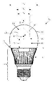
Fig. 1 shows a side-view of a light source 10 according to the invention. The
light source 10 comprises a light emitter 20 which is positioned inside a
translucent outer
envelope 30. The light emitter 20 comprises a light emitting device 40 (see
Fig. 4) which is at
least partially surrounded by a translucent inner envelope 50 comprising a
diffuser (not
10 indicated) for diffusing at least a part of the light emitted by the
light emitting device 40. The
diffuser may be integrated in the wall of the inner envelope 50 or may be
applied as a layer to
an inner wall or an outer wall of the inner envelope 50. A diameter di of the
translucent inner
envelope 50 is smaller than a diameter do of the translucent outer envelope
30. The
translucent outer envelope 30 is connected to a base 60 which is usually not
translucent.
15 Furthermore, the translucent outer envelope 30 comprises a symmetry axis
S. In Fig. 1 also
an imaginary base-plane P is indicated via a dash-dotted line. This imaginary
base-plane P is
defined substantially perpendicular to the symmetry axis S and intersects with
a connection
point C which is part of the translucent outer envelope 30. The connection
point C being a
light transmitting part of the translucent outer envelope 30 at an interface
between the
translucent outer envelope 30 and the base 60 at a furthest distance from a
center M of the
translucent outer envelope 30. The exact location of the center M of the
translucent outer
envelope 30 is not required as it only is used to define a direction in which
the furthest
distance has to be found.
The light emitter 20 is positioned inside the translucent outer envelope 30 at
a
distance D from the imaginary base-plane P away from the base 60.
The imaginary base-plane P defines a rim which physically blocks light which
is emitted by the light emitter inside the outer envelope. As the imaginary
plane intersects
with the connection point C which is defined as a translucent point nearest to
the base, the
connection point is the closest point to the base which still emits light. By
defining a distance
between the light emitter and the base via the imaginary base-plane P, the
point at which the
increase of the emission distribution commences compared to the embodiment
shown in the
non-prepublished patent application as cited in the introductory part is
defined.
An effect of the light source 10 according to the invention is that the
emission
profile (see Fig. 2) of the light source 10 according to the invention is
increased. Because the
CA 02760767 2011-11-02
WO 2010/128419
PCT/1B2010/051793
16
light emitter 20 according to the invention comprises the translucent inner
envelope 50
comprising the diffuser, and because the light emitter 20 is positioned at the
distance D from
the imaginary base-plane P, more light is emitted in a direction towards the
imaginary base-
plane P, thus increasing the emission profile of the light source 10 in a
direction towards the
imaginary base-plane P. Generally each scattering point in a diffuser causes
part of the
impinging light to be scattered substantially in multiple directions, and in
case of isotropic
scattering even in all directions. "Elevating" this diffuse light emitter 20
from the base 60
will increase the angles at which light is emitted from the light source 10
and as such
increases the emission profile.
When the distance D between the light emitter 20 and the imaginary base-
plane P would be zero, no "elevation" of the light emitter 20 would be present
and the rim of
the base 60 will block a substantial part of the light from being emitted by
the light source 10
at angles larger than 90 degrees from a direction along the symmetry axis S
pointing away
from the base towards the outer envelope, which corresponds with an emission
distribution
that is not substantially larger than 180 degrees. In such an embodiment,
substantially no
light will be emitted towards the imaginary base-plane P. By positioning the
light emitter 20
at the distance D from the imaginary base-plane P, the scattered light from
the diffuser of the
inner envelope 50 will ensure that a larger contribution of scattered light
will be emitted
towards the imaginary base-plane P, thus increasing the emission distribution
to above 180
degrees.
A further benefit of the light source 10 according to the invention is that
the
light emitter 20 inside the outer envelope 30 at the distance D from the base
60 may be used
to generate an appearance of the light source 10 ¨ during operation ¨ as if
the light source 10
would comprise a filament. In incandescent light sources, the filament emits
very high
intensity light. As the human eye is not able to handle such high intensities,
this filament
inside the known incandescent light sources is often observed by the human eye
as a glowing
sphere inside a glass envelope. By applying the inner envelope 20 at
substantially the same
location as where the glowing sphere is perceived in an incandescent light
source, the
appearance, in operation, of an incandescent light source by the light source
10 according to
the invention may be very well imitated. This may be especially beneficial in
optical designs
where the location of the filament in the incandescent light source is
important. The light
source 10 according to the invention may directly be used as a retrofit lamp
having
substantially similar characteristics as the incandescent light source while
being much more
CA 02760767 2011-11-02
WO 2010/128419 PCT/1B2010/051793
17
energy efficient, especially when light emitting diodes 40 (see Fig. 4) are
used as light
emitting device 40.
The distance D between the base and the light emitter 20 may be chosen such
that the beam width is at least 220 degrees FWHM. This typically results in
that the center of
gravity of the inner envelope 50 is located at a position between 1/4 of a
height of the outer
envelope 30 relative to the base 60 of the light source 10, and 3/4 of the
height of the outer
envelope 30, preferably between 1/3 of a height of the outer envelope 30
relative to the base
60 of the light source 10, and 2/3 of the height of the outer envelope 30. The
height of the
outer envelope 30 is measured in a direction of the symmetry axis S.
The geometry of the components is chosen such that the beam width is at least
220 degrees FWHM. This may be achieved by selecting a geometry of the
components in
which an angle between a line (not indicated) connecting the point on the
surface of the inner
envelope at the maximum diameter of the inner envelope and the connection
point C, and the
symmetry axis S should be smaller than 90 degrees, preferably smaller than 45
degrees,
preferably smaller than 30 degrees. In the embodiment shown in Fig.1 the angle
defined in
the previous line is approximately 25 degrees, and this lamp results in a beam
angle of about
250 degrees FWHM. In addition, the diffusivity of the inner envelope 20
preferably is high,
preferably FWHM larger than 80 degrees.
The inner envelope 20 comprises a cut-out portion 55 for accommodating the
light emitting device 40. In the embodiment shown in Fig. 1, the cut-out
portion 55 is formed
as a planar cut through a spherical inner envelope 20. Of course, also other
shapes of the cut-
out portion 55 may be possible. A diameter di of the inner envelope 20 is
larger than a
diameter dc of the cut-out portion 55. As a result, the inner envelope 20
bulges outward at the
intersection between the inner envelope 20 and the circuit board 70 (see Fig.
4B) which
comprises the light emitting device 40. This initial extension of the inner
envelope 20 causes
part of the diffuser at the inner envelope 20 to substantially face the
imaginary base-plane P.
As such, more light will be scattered towards the imaginary base-plane P thus
ensuring that a
larger part of the light of the light emitting device 10 is emitted towards
the imaginary base-
plane P. As such the emission distribution of the light source 10 may be
further enhanced.
Although the inner envelope 20 in the embodiments of the light source 10, 12
all have a spherical shape, the inner envelope 20 may, of course have any
shape. The benefit
of this spherical shape is that the glowing filament at relatively high
intensity is also
perceived as a glowing spherical ball and thus using this spherical inner
envelope 20 may
cause the light source in operation to closely resemble incandescent light
sources.
CA 02760767 2011-11-02
WO 2010/128419 PCT/1B2010/051793
18
The light emitter 20 is positioned inside the outer envelope 30 via the
connection means 80. The connection means 80 may of course have any shape.
However, the
connection means 80 may preferably have a hollow cone-shape which expands from
the
circuit board 70 on which the light emitting device 40 is connected towards
the base. The
width of the cone-shaped connection means 80 preferably is smaller than the
diameter of the
base 60 such that no light emitted by the light emitter 20 is blocked by the
connection means
80. Inside the hollow cone-shaped connection means 80 additional electronics
may be located
for converting power to a suitable level for the used light emitting device 40
and may
comprises specific electronics for driving the light emitting device. 40.
Finally, the
connection means 80 may have a heat-conductive function. When using light
emitting diodes
40 as light emitting devices 40, the cooling of the light emitting diodes 40
is an important
issue. Inside the light emitter 20 there is no space to have cooling means for
reducing and/or
limiting the temperature of the light emitting devices 40 inside the light
emitter 20. When
using the connection means 80, the connection means 80 may be used to conduct
the heat
away from the light emitting devices 40, for example, towards the base 60
where additional
heat transfer means 90 may be present.
The base 60 is connected to the outer envelope 30. This base 60 comprises the
heat transfer means 90 which in the current embodiment are constituted of
cooling fins 90
which conduct the heat from the light emitting devices 40 via the connection
means 80 to the
environment. As mentioned before, also other heat transfer means 90 may be
used such as
heat exchangers (not shown) which exchange heat with a cooling fluid, for
example, a
cooling liquid. The base 60 as shown in Fig. 1 also comprises a winding
similar to the
windings used for connecting the known incandescent light sources to an
external power
source (not shown). As such the light source 10 may directly be used as
retrofit for the well
known incandescent light sources having such similar winding. Of course also
other means
for connecting the light source 10 to some external power source may be used.
Fig. 2 shows a graph indicating the emission distribution of the light source
10
according to the invention shown in Fig. 1. In the graph shown in Fig. 2 the
intensity of the
light is plotted along the vertical axis of the graph and the azimuthal angle
along the
horizontal axis. The width of the beam is defined at half the maximum
intensity as is
indicated with the double arrow 110 in the center of the light intensity curve
100. The dashed
lines 120a, 120b originating from the intersection point between the double
arrow 110 and
the light intensity curve 100 define the angular distribution of the light
source 10 at full width
at half maximum. In the current example the width of the emission distribution
of the light
CA 02760767 2011-11-02
WO 2010/128419 PCT/1B2010/051793
19
source 10 is 254 degrees FWHM for a light source 10 having a distance D (see
Fig. 1)
between the base 60 and the light emitter 20 of 16,5 millimeter. This is
equivalent with a
position of the center of gravity of the inner envelope 50 of 1/2 the height
of the outer
envelope 30.
Figs. 3A and 3B show side views of different embodiments of the light source
10, 12 according to the invention. In the different embodiments shown in Figs.
3A and 3B the
outer envelope 30, 32 comprises a further diffuser. The further diffuser is
configured for
redirecting part of the light transmitted by the outer envelope 30, 32. The
diffuser comprises
a predefined diffusivity which influences the appearance of the light source
10, 12 according
to the invention. The diffusivity is defined by scattering behavior of a
collimated pencil beam
using the parameter Full Width at Half Maximum of the transmitted beam. The
collimated
pencil beam comprises a FWHM of the collimated beam of less than 1 degree. The
FWHM
can be between 5 and 120 degrees. Preferably the diffusivity is between 5 and
40 degrees in
order to have some additional redirecting, have the filament effect, and still
have a high
efficiency. In Fig. 3A the diffusivity is highest which results in the details
of the inner
envelope 50 are hardly visible. As the inner envelope 50 typically comprises a
luminescent
material converting blue light into yellow light, the inner envelope 50
typically has a yellow
appearance when the light source 10, 12 is switched off. This is not
preferred. By choosing a
further diffuser having a relatively high diffusivity (FWHM between 30 and 120
degrees), the
details of the inner envelope 50 are less visible, which includes the yellow
appearance of the
inner envelope 50. In Fig. 3B the further diffuser has a lower diffusivity
(FWHM between 5
and 30 degrees). As a result the details inside the inner envelope are
relatively well visible
and the efficiency is higher. The beam angle of the light emitted from the
light source 10 will
be smaller than in case of the higher diffusivity as in Fig. 3A, but still
larger than in light
sources of the prior art.
To further reduce this yellow appearance of the inner envelope 50 in the light
source 10, 12 according to the invention, the outer wall of the inner envelope
50, being the
wall of the inner envelope 50 facing the outer envelope 30, 32, may comprise a
white
diffusing layer. This white diffusing layer does only marginally influence the
color of the
light emitted by the light source 10, 12. Still the appearance of the inner
envelope 50 when
the light source 10, 12 is in the off-state, may be clearly altered.
Figs. 4A and 4B show cross-sectional views at different detail levels of the
light source 10 according to the invention. Fig. 4A shows a cross-sectional
view of the whole
light source 10, and Fig. 4B shows a detailed cross-sectional view of the
inner envelope 50
CA 02760767 2011-11-02
WO 2010/128419 PCT/1B2010/051793
comprising the light emitting devices 40 being light emitting diode devices
40. The
intersection point To between the outer envelope 30 and the symmetry axis S is
also indicated
as the top To of the outer envelope 30, indicated in Fig. 4A. The intersection
point Ti between
the inner envelope 50 and the symmetry axis S is also indicated as the top Ti
of the inner
5 envelope 50, indicated in Fig. 4B.
In Fig. 4A it can clearly be seen that the connection element 80 is a cone-
shaped connection element 80 widening from the light emitter 20 toward the
base 60.
Furthermore, the cone-shaped connection element 80 is hollow and may provide
space for
additional electronics, for example, for converting power to a suitable level
for the used light
10 emitting device 40. Furthermore, the connection means 80 may have a heat-
conductive
function for transporting heat away from the light emitting devices 40, for
example, towards
the base 60 where additional heat transfer means 90 may be present such as
cooling fins 90.
The circuit board 70 preferably is a flat circuit board 70 as shown in Fig. 4B
as
may be produced relatively cheap. However, the circuit board 70 may also be
constituted of
15 several circuit boards (not shown) which are arranged at different
angles with respect to the
symmetry axis S and/or with respect to each other. As can also be seen from
Fig. 4B the
circuit board 70 may comprise one light emitting diode 40 but may also
comprise more than
one light emitting diode 40. The circuit board 70 may further comprise a
reflective and/or
luminescent layer on a side of the circuit board 70 which faces the inner
envelope 50. In such
20 an embodiment, the reflective layer may, for example, be used to enable
recycling of light
and the luminescent material may be used to fine-tune the color emitted by the
light source
10 and/or may be used to correct the emission characteristic of the light
emitting diode 40
applied to the circuit board 70. The light emitting devices 40 may, for
example, emit blue
light or may emit any other color of light and may, for example, comprise
phosphor-
converted light sources 40 such as phosphor-converted light emitting diodes
40.
The inner envelope 50 may, for example, be manufactured via injection
molding of a transparent polymer such as Polycarbonate which comprises
luminescent
material mixed in the Polycarbonate before molding. The luminescent material
may also be
applied after the Polycarbonate has been molded as a layer on the inner and/or
outer surface
of the inner envelope 50. Optionally an additional diffusive material such as
Ti02, Si02 or
A1203 may be applied inside the Polycarbonate and/or as a layer on top of the
Polycarbonate.
Alternatively, the inner envelope 50 may be made from e.g. flush coating or
spray coating of
a glass or plastic transparent or translucent concave substrate in which the
luminescent
CA 02760767 2011-11-02
WO 2010/128419
PCT/1B2010/051793
21
material and optionally additional diffusive material may be present in a
suitable (polymer)
matrix.
Alternatively, the inner envelope 50 may, for example, be manufactured via
injection molding of a transparent polymer such as a silicone rubber which
comprises
luminescent material mixed in the silicone rubber before setting. Optionally
an additional
diffusive material such as Ti02, Si02 or A1203 may be applied inside the
silicone rubber.
Figs. 5A and 5B show cross-sectional views at different light sources 14, 16
according to the invention in which the outer envelope 30 has been omitted.
The outer
envelope 30 is not indicated in the Figs. 5A and 5B to more clearly show the
shape of the
inner envelope 52 in Fig. 5A and to more clearly show the specific arrangement
of the light
emitting devices 40 in Fig. 5B. However, in operation, an outer envelope 30 is
present as
indicated in Fig. 1 and as indicated in the claims. In the embodiment shown in
Fig. 5A an
elongated inner envelope 52 is shown in which the dimension of the inner
envelope 52 along
the symmetry axis S is larger than the dimension of the inner envelope 52 in a
direction
perpendicular to the symmetry axis S. Such an inner envelope 52 results in a
different
filament effect compared to the previous embodiments in which the inner
envelope 50
comprises a substantially spherical shape. In the embodiment shown in Fig. 5B
the light
emitting device 40 is constituted of a plurality of light emitting diodes 40
which are arranged
on different circuit boards 70, 72a, 72b which are arranged at different
angles with respect to
the symmetry axis S and with respect to each other. Such an arrangement
generates a further
increased spatial emission distribution of the light source 16 as more light
is emitted toward
the base-plane P (not shown in Fig. 5B). To obtain a substantially homogeneous
color
distribution the plurality of light emitting diodes preferably emit light of
substantially
identical color.
The outer envelope 30 may for example be made of transparent glass. The
proper diffusivity may be achieved by e.g. sand blasting or etching of the
inner and/or outer
surface, or by e.g. flush coating or spray coating with a proper diffusive
material such as
Ti02, 5i02 or A1203 in a suitable (polymer) matrix. After the coating process,
the matrix
material may be removed by heating. Alternatively, the outer envelope 30 may
be made of a
translucent plastic such as Polycarbonate or silicone rubber containing
additional diffusive
material. The outer envelope 30 may be manufactured by e.g. injection blow
molding,
injection molding or compression molding, depending on the properties of the
materials used.
In one embodiment according to the invention, a red-orange nitride phosphor
is applied to the inner envelope 50 (i.e., the remote luminescent element),
while on the circuit
CA 02760767 2011-11-02
WO 2010/128419 PCT/1B2010/051793
22
board 70 at least a blue emitting light emitting diode 40 is applied and a
yellow-green
phosphor is applied to provide whitish light emitted from the inner envelope
50.
In a further embodiment, a yellow-green phosphor, e.g. a yellow-green garnet
phosphor, is applied to the inner envelope 50 and a red-orange phosphor, e.g.
a red-orange
nitride phosphor, is applied on the circuit board 70 or on the light emitting
diode 40 at the
proximity of the blue light emitting light emitting diode 40.
A further embodiment comprises a mixture of a red-orange and a yellow-green
phosphor applied to the inner envelope 50, while on the circuit board 70 at
least a blue light
emitting light emitting diode 40 is provided.
Alternatively, in an embodiment, a red-orange phosphor, for example, a red-
orange nitride phosphor is applied to the inner envelope 50 and a yellow-green
phosphor, for
example, a yellow-green garnet phosphor, is applied in the outer envelope 30,
while the
circuit board 70 comprises at least a blue light emitting light emitting diode
40.
In a further embodiment, a blue light emitting light emitting diode 40 and a
red
light emitting light emitting diode 40 are both mounted on the circuit board
70, while the
inner envelope 50 comprises at least a yellow-green phosphor.
In a further embodiment, a blue light and red light emitting light emitting
diode 40, comprising a luminescent material that emits red-orange light upon
irradiation with
blue light, is mounted on the circuit board 70, while the inner envelope 50
comprises at least
a yellow-green garnet phosphor.
In an even further embodiment, white light emitting light emitting diodes 40
are mounted on the circuit board 70, while the inner envelope 50 comprises a
diffusive
material. This embodiment does not comprise luminescent materials applied to
the inner
envelope 50 nor to the outer envelope 30 while still the filament effect is
present.
In all configurations, the red light emitting device 40 or the red luminescent
material has a peak wavelength of at least 600 nm, preferably at least 610 nm
and maximum
peak wavelength of 660 nm, preferably 650 nm, most preferably 640 nm.
The garnet phosphor typically comprises the general formula:
(YxLui_)3A15012:Ce (0.x.1),
and the nitride phosphor typically comprises the general formula:
(CaxSryBai_x_y)AlSiN3:Eu (0.,(1, 0.3[1-x), or
(CaxSryBai_x_y)2Si5N8:Eu (0,(1,13.31-x)
CA 02760767 2011-11-02
WO 2010/128419 PCT/1B2010/051793
23
It should be noted that the above-mentioned embodiments illustrate rather than
limit the invention, and that those skilled in the art will be able to design
many alternative
embodiments without departing from the scope of the appended claims.
In the claims, any reference signs placed between parentheses shall not be
construed as limiting the claim. Use of the verb "comprise" and its
conjugations does not
exclude the presence of elements or steps other than those stated in a claim.
The article "a" or
"an" preceding an element does not exclude the presence of a plurality of such
elements. The
invention may be implemented by means of hardware comprising several distinct
elements.
In the device claim enumerating several means, several of these means may be
embodied by
one and the same item of hardware. The mere fact that certain measures are
recited in
mutually different dependent claims does not indicate that a combination of
these measures
cannot be used to advantage.