Note: Descriptions are shown in the official language in which they were submitted.
CA 02761491 2011-12-13
W6259
- 1 -
CONTROL SYSTEM AND NODE ADDRESS SETTING METHOD FOR CONTROL
SYSTEM
BACKGROUND OF THE INVENTION
This invention relates to a control system and a node address setting method
for
the control system, in which plural devices as control components are
interconnected to form a
redundant system and mutual communication among the plural devices can be
effectuated by
assigning individual node addresses to the devices.
In a control system used for the control of a plant, communication among the
control components of the system (hereafter referred to as control
communication) is vital
concern for the coordinated operation of the control system. Accordingly, it
is essential to
assign unique addresses (hereafter referred to as node addresses) to the
respective control
components so that the control components can be discriminated from one
another by the node
addresses.
Regarding such a node address setting method is known JP-A-2001-339392,
according to which the node address of a controller is set by using a rotary
switch. Also, JP-A-
2001-236103 discloses a node address setting method used for the control
communication to be
performed among field devices that constitute a whole control system.
According to this
method, each node address is defined as the combination of the device ID of
each field device
and the network ID of the connector coupled to that particular field device.
SUMMARY OF THE INVENTION
In general, a control system must have a high reliability so that it can
continue to
run even when part of the system fails. Such a reliable control system is
usually realized as a
redundant system comprising two processing units and plural input/output
devices.
However, as disclosed in JP-A-2001-339392, the known address setting method
can set only addresses from OX0 up to OXF through the use of a single rotary
switch, and
therefore plural rotary switches must be used in such a control system as a
redundant control
system including a number of control components each of which must be provided
with a node
address. Accordingly, a problem arises that the number of steps for setting
node addresses
increases, thereby increasing the probability of man-made errors being
incurred in setting node
addresses.
Further, in the case where the node address setting method as disclosed in JP-
A-
2001-236103 is used in a redundant control system, if two processing units
erroneously set
CA 02761491 2014-04-02
- 2 -
different addresses, the two different node addresses are transferred to
input/output devices,
and therefore a problem arises that there is no determining which of the two
node addresses is
to be adopted.
The object of this invention, therefore, is to provide a control system and a
node address setting method for the control system, in which node addresses
can be set with a
minimal number of setting steps and effectively prevent man-made errors that
may be
incurred in setting node addresses.
Certain exemplary embodiments can provide a control system comprising:
processing units for executing processing operations necessary for a
controlled system and
outputting control commands; a plurality of I/O devices for receiving the
control commands
and outputting the control commands to the controlled system; and duplicate
intermediary
units connected between the processing units and the plural I/O devices via
transmission lines,
and which relay the control commands from the processing units to the I/O
devices, wherein
each of the duplicate intermediary units includes an upper address output
device which
generates upper address data and outputs the upper address data to the I/O
devices; and
each of the I/O devices includes an upper address comparator for comparing the
upper address
data inputted from one of the duplicate intermediary units with the upper
address data
inputted from the other duplicate intermediary unit, an upper address setting
unit for selecting
upper address data based on the comparison, and a line control unit for
forming a node
address for a particular I/O device by merging selected upper address data and
lower address
data determined by the particular I/O device.
Certain exemplary embodiments can provide a control system which includes
processing units for outputting control commands to a controlled system,
intermediary units
for relaying the outputs of the processing units, and I/O devices for
outputting the relayed
control commands to the controlled system, and in which the processing units,
the
intermediary units and the I/O devices are interconnected with one another via
transmission
lines, wherein the intermediary unit includes an upper address setting section
for outputting
upper address data generated in itself to the I/O devices, and wherein the I/O
device includes
plural reception circuits for receiving the upper address data; a state
determination section for
CA 02761491 2014-04-02
- 2a -
determining modes of the transmission lines on the basis of reception
conditions of the
reception circuits; and a line control unit for setting a node address of the
I/O device by
merging the upper address data received from the transmission lines considered
available on
the basis of a result determined by the state determination section and a
lower address data set
by the I/O device.
Certain exemplary embodiments can provide a node address setting method
used for a control system, wherein an upper address serving as a part of a
node address for
one of I/O devices is set by each of duplicate intermediary units that input
the outputs of
processing units and then output them to the I/O devices; the I/O device
compares the upper
addresses set by the respective duplicate intermediary units with one another;
the upper
address is selected on the basis of the result of comparison; and the node
address for the I/O
device is set by merging the selected upper address and a lower address set by
the I/O device.
According to other embodiments, since the node address of each I/O device
can be determined on the basis of the node address data generated by the
intermediary unit,
node addresses can be set without increasing the number of node address
setting steps.
Further, since each I/O device compares the two pieces of node address data
received from the
intermediary units with each other and determines the node address for itself,
then it becomes
possible to flexibly cope with erroneous setting of node addresses.
Other objects, features and advantages of the invention will become apparent
from the following description of the embodiments of the invention taken in
conjunction with
the accompanying drawings.
CA 02761491 2011-12-13
W6259
- 3 -
BRIEF DESCRIOTION OF THE DRAWINGS
Fig. 1 shows in block diagram the entire structure of a redundant control
system
according to this invention;
Fig. 2 illustrates node addresses (in hexadecimal notation) for various units
and
devices used in the redundant control system according to this invention shown
in Fig. 1;
Fig. 3 shows the way of communication over data lines and the format of a
transfer frame;
Fig. 4 shows the format of a transfer frame sent over serial lines;
Fig. 5 shows in block diagram the circuit structure of a frame reception
circuit;
Fig. 6 shows in block diagram the circuit structure of a timeout counter;
Fig. 7 illustrates address reception completion patterns;
Fig. 8 shows in block diagram the circuit structure of an upper node address
setting circuit;
Fig. 9 shows in block diagram the circuit structure of a communication control
section in a data line control circuit;
Fig. 10 shows the relationship among subsystem 1/2/1-2 states, combinations of
line mode data from processing unit (primary system) (1) and processing unit
(standby system)
(2), and corresponding communication states of data lines; and
Fig. 11 shows the format of a node address for an intermediary unit A(3) or an
intermediary unit B (4).
DESCRIPTION OF THE EMBODIMENTS
An embodiments of this invention will be described below with reference to the
accompanying drawings.
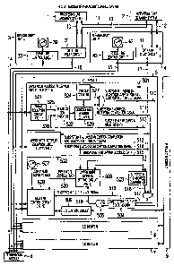
Fig. 1 schematically shows a redundant control system as an embodiment of this
invention. The redundant control system shown in Fig. 1 comprises a processing
unit (primary
system) (1), a processing unit (standby system) (2), an intermediary unit
A(3), an intermediary
unit B (4), N input/output devices (I/O device A (5), I/O device B (6), ,
and I/0 device N
(7)), and a termination module (8). The processing unit (primary system) (1),
the processing
unit (standby system) (2), the intermediary unit A (3) and the intermediary
unit B (4) are
interconnected by data lines (10 ¨ 13). The intermediary unit A (3), the
intermediary unit B (4),
and the N input/output devices are interconnected by data lines (16, 17) and
serial lines (14, 15)
such as RS 232C. The termination module (8) is connected at the ends of the
serial lines (14,
15) and the data lines (16, 17). It is to be noted here that the intermediary
unit A(3) and the
CA 02761491 2011-12-13
W6259
- 4 -
intermediary unit B (4) are of identical design. Communication through the
data lines (10 ¨ 13,
16, 17) is performed with such frames as described later.
The processing unit (primary system) (1) and the processing unit (standby
system)
(2) operate by receiving information from a controlled system such as, for
example, a turbine (9)
installed in a 24-hour-run electric power plant, and generate control
commands. The I/O device
A (5), I/0 device B (6),
...................................................... , and I/0 device N (7)
exchange inputs and outputs directly with the
controlled system (9) via a data line control circuit (508) and an
input/output control circuit
(509); output control signals from the processing unit (primary system) (1)
and the processing
unit (standby system) (2), to the controlled system (9); and send data
obtained from the
controlled system (9), to the processing unit (primary system) (1) and the
processing unit
(standby system) (2). In the actual component arrangement, the processing unit
(primary
system) (1) and the processing unit (standby system) (2) are sometimes placed
distantly
separated from the I/O device A (5), I/O device B (6), , and I/0 device N
(7), and in such a
case the intermediary unit A (3) and the intermediary unit B (4) serve to
relay between (the
processing unit (primary system) (1) and the processing unit (standby system)
(2)) and (the I/O
device A (5), I/O device B (6), .. , and I/0 device N (7)). Moreover, the
processing unit
(primary system) (1) and the processing unit (standby system) (2) are
connected with additional
intermediary units having the same design as the intermediary unit A (3) and
the intermediary
unit B (4), and additional input/output devices, though they are not shown in
Fig. 1.
In order that the I/0 device A (5), I/0 device B (6), ....... , and I/O
device N (7)
may perform control communication with the processing unit (primary system)
(1) and the
processing unit (standby system) (2), it is essential to assign individual
addresses (hereafter
referred to as node addresses), which serve to distinguish one I/O device from
another, to the I/O
device A (5), I/O device B (6), .. , and I/0 device N (7), respectively.
According to this
invention, in a redundant control system, the upper portion of a node address
(hereafter referred
to as upper node address) for each of the I/O device A (5), I/O device B (6),
.. , and I/O device
N (7) is set by the intermediary unit A (3) or the intermediary unit B (4),
whereas the
corresponding lower portion of the node address (hereafter referred to as
lower node address) is
set by the I/0 device A (5), I/0 device B (6), ..............................
, and I/O device N (7). Consequently, the
combination of the upper and lower node addresses is defined as identifying a
particular I/0
device, and the I/O device A (5), I/O device B (6),
........................... , and I/O device N (7) communicate with
the processing unit (primary system) (1) and the processing unit (standby
system) (2) by using
such composite node addresses. Accordingly, even when a number of input/output
devices are
involved, the setting of node addresses becomes possible without providing
plural rotary
CA 02761491 2011-12-13
W6259
- 5 -
switches for each I/0 device.
Fig. 2 shows node addresses (in hexadecimal notation) assigned to respective
devices according to this embodiment. As shown in Fig. 2, node address "0X800"
is assigned
to the processing unit (primary system system) (1), "0X801" to the processing
unit (standby
system system) (2); "OXI3DO" to the intermediary unit A (3); "OXB50" to the
intermediary unit B
(4); "0X500" to the IJO device A (5); and "OX501" to the I/O device B (6). And
communication
via the data lines (10 ¨ 13, 16, 17) is performed with frames having those
node addresses, as
shown in Fig. 3.
Fig. 3 shows the format of each frame transmitted and received through the
data
lines among the processing unit (primary system) (1), the processing unit
(standby system) (2),
the I/0 device A (5), I/0 device B (6), , and 110 device N (7). The lower
part of Fig. 3
shows the format of a transfer frame, which includes a preamble for frame
synchronization
throughout data lines, two upper flag fields for upper flags indicating the
start of this frame, a
destination address field, a source address field, data field, a CRC code
field, a lower flag field
for lower flag indicating the end of this frame. As shown in the upper part of
Fig.3, when the
processing unit (primary system) (1) or the processing unit (standby system)
(2) transmits such a
frame as described above to the I/O device (5), node addresses "OX500" and
"OX00" are set in
the destination address field and the source address field, respectively, and
the transmission
frame (701) loaded with those node addresses is transmitted. If the I/O device
A(S) has node
address "OX500" assigned thereto, it receives the frame having "OX500" set in
its destination
address field. Then, the I/O device A (5) completes a response frame (702) by
setting node
addresses "OX000" and "0X500" in the destination address field and the source
address field of
the above described frame, respectively, and transmits the thus completed
response frame. The
I/0 device B (6), too, communicates with the processing unit (standby system)
(2) or the
processing unit (standby system) (2) in the same manner.
Described below will be the process flow of how communication among the
processing unit (primary system) (1), the processing unit (standby system)
(2), the I/O device A
(5), I/O device B (6), .. , and I/O device N (7) is started after completing
frames each having a
12-bit node address as shown in Fig. 2, consisting of an 8-bit upper node
address and a 4-bit
lower node address.
It should be noted here that the setting of node addresses in the I/O device A
(5),
I/0 device B (6), .. , and I/O device N (7) is performed once when the
control system is
powered on, and that the I/O devices keep on having the once set node
addresses until the system
is turned off and again turned on. It should also be noted that when the
system is turned on, a
CA 02761491 2011-12-13
,
W6259
- 6 -
shift register (5211), a register A(5213), a register B (5214) and an upper
node address setting
circuit (506) are all initialized to "0", whereas a coincidence number counter
(523), a subsystem
1 timeout counter (524), a subsystem 2 timeout counter (528) are also reset to
"0".
How node addresses are set in the respective I/0 device A (5), I/0 device B
(6),
.. , and I/0 device N (7), is of the same process, and therefore description
of node address
setting will be given only to the I/O device A (5). First, in the intermediary
unit A (3) and the
intermediary unit B (4), the 8-bit upper node address "0X50" of the I/O device
A (5) is generated
by using rotary switches (32, 42). Then, serial line control circuits (33, 34)
transfer the 8-bit
upper node address "OX50" set by the rotary switches (32, 42) cyclically to
the I/O device A (5)
via the serial lines (14, 15).
It is to be noted here that transfer frames as shown in Fig. 4 are transferred
through the serial lines (14, 15). The content of the transfer frame consists
of a start flag
indicating the start of the transfer frame, a synchronizing bit indicating the
start of the data field
of the transfer frame, baud rate, upper node address data, a parity bit, and
an end bit indicating
the end of the data field of the transfer frame. The transfer frames include
transmission frames
(701) and response frames (702), and both the transmission frame (701) and the
response frame
(702) are transferred in the format (710) of the transfer frame shown in Fig.
4.
The rotary switches (32, 42) are also used to set node addresses for the
intermediary unit A (3) and the intermediary unit B (4). Fig. 11 shows the
format of a node
address to be assigned to the intermediary unit A (3) or the intermediary unit
B (4). The node
address for the intermediary unit is determined by merging upper 4 bits
representing the value
"OXB" indicating the type of device, an intermediate 1 bit representing the
value "OXO" or "OX1"
determined depending on the subsystem to which the intermediary unit is
connected, and lower 7
bits representing the value "0X50" denoting the lower 7 bits of the value set
by the rotary switch
(32, 42). Thus, the same switches can be utilized both as the switches for
setting the node
addresses of the intermediary unit A (3) and the intermediary unit B (4) and
as the switch for
setting the upper node address of the I/0 device A (5), so that cost can be
reduced and that man-
made errors can be reduced in number.
In the I/0 device A (5), an upper node address reception circuit (subsystem 1)
(501) receives a frame transferred from the intermediary unit A(3) via the
serial line (14), and an
upper node address reception circuit (subsystem 2) (502) receives a frame
transferred from the
intermediary unit B (4) via the serial line (15). The circuit structure of the
upper node address
reception circuit (subsystem 1) (501) is the same as that of the upper node
address reception
circuit (subsystem 2) (502). Hereafter, therefore, only the upper node address
reception circuit
CA 02761491 2011-12-13
W6259
- 7 -
(subsystem 1) (501) is described and the upper node address reception circuit
(subsystem 2)
(502) will be described only when it is necessary to do so.
Regarding the upper node address reception circuit (subsystem 1) (501), the
shift
register (5211) in a frame reception circuit (521) shown in Fig. 5 receives
upper node address
data "0X50". Then, the received upper node address data "0X50" is subjected to
parity check
(5212). If the result of the parity check is "true", the address data "0X50"
is stored in a register
A (5213). If, on the other hand, the result of the parity check is "false",
the data "0X50" is
discarded and nothing is written in the register A (5213).
Subsequently, the shift register (5211) receives next upper node address data
"0X50", and again the address data "0X50" is to be stored in the register A
(5213). In this case,
however, the next address data "0X50" is stored in the register A (5213) only
after the previous
upper node address data "OX50" has been shifted to a register B (5214). When
the values in
both the register A(5213) and the register B (5214) are renewed, the address
data stored in both
the register A (5213) and the register B (5214) are outputted to an address
comparator (522).
The address comparator (522) compares the inputted address data (525) of the
register A with the inputted address data (526) of the register B, that are
respectively "OX50" and
"0X50", which are coincident with each other. This coincidence causes a
coincidence number
counter (523) to count up by unity. But if the inputted address data (525) of
the register A and
the inputted address data (526) of the register B are not coincident with each
other, the content of
the coincidence number counter (523) is reset to zero.
The coincidence number counter (523) outputs a subsystem 1 address reception
completion signal (511) when the content of the counter (523) becomes equal
to, for example,
"3". And once the coincidence number counter (523) has counted up to "3", it
stops counting
up further and retains the value "3" until it has been reset to zero. Thus, a
temporary error in
the upper node address data can be avoided by ascertaining the multiple
reception of the same
data through the use of the coincidence number counter (523).
The operation of a timeout counter (524) will be described below with
reference
to Fig. 6 which shows the circuit structure of the timeout counter (524). The
subsystem 1
timeout counter (524) starts counting up in response to the subsystem 1
address reception
completion signal (511), which serves as a triggering signal, outputted from
the coincidence
number counter (523). The upper block diagram in Fig. 6 corresponds to the
subsystem 1
timeout counter (524), which is triggered by the subsystem 1 address reception
completion signal
(511) to start counting up, and stops counting in response to a subsystem 2
address reception
completion signal (514). When the content of a counter (5241) becomes equal to
any of the
CA 02761491 2011-12-13
W6259
- 8 -
values ranging from 500ms to 600ms, a timeout determiner (5242) decides that a
timeout is
reached, and then outputs a subsystem 2 timeout signal (527).
The lower block diagram in Fig. 6 corresponds to a subsystem 2 timeout counter
(528), which is triggered by the subsystem 2 address reception completion
signal (514) to start
counting up, and stops counting in response to the subsystem 1 address
reception completion
signal (514). When the content of a counter (5281) becomes equal to any of the
values ranging
from 500ms to 600ms, a timeout determiner (5282) decides that a timeout is
reached, and then
outputs a subsystem 1 timeout signal (529).
When the address reception in the subsystem 1 finishes before the address
reception in the subsystem 2 has been completed, the subsystem 1 timeout
counter (524) starts
counting up and the subsystem 2 timeout counter (528) stops counting
simultaneously. Now,
when the address reception in the subsystem 2 finishes before the timeout
period lapses, the
subsystem 2 timeout counter (528) tends to start counting up. However, since
the subsystem 2
timeout counter (528) is already in the dormant state in response to the
subsystem 1 address
reception completion signal (511), the subsystem 2 timeout counter (528) will
not start counting.
Further, since the subsystem 1 timeout counter (524) is maintained in the
dormant state so that
the subsystem 2 timeout signal (527) is prevented from being outputted, then
the address
reception is completed in both the subsystems 1 and 2.
When the subsystem 1 timeout counter (524) outputs the subsystem 2 timeout
signal (527), only the address reception in the subsystem 1 is meant to be
finished. Also, the
fact that the address reception in the subsystem 2 finishes before the address
reception in the
subsystem 1, means that either address receptions in both the subsystems 1 and
2 have been
completed, or address reception only in the subsystem 2 has been completed. If
none of the
timeout counters in the subsystems 1 and 2 receives an address reception
completion signal, both
the timeout counters keep waiting until at least one of the subsystem 1
address reception
completion signal and the subsystem 2 address reception completion signal is
inputted.
Fig. 7 is a table showing patterns of address reception completion
corresponding
to various ordered combinations among the subsystem 1 address reception
completion, the
subsystem 2 address reception completion, the subsystem 1 timeout, and the
subsystem 2
timeout. If only the address reception in the subsystem 1 has been completed,
a subsystem 1
address reception completion and subsystem 2 timeout signal (510) is generated
by making the
logical product of the subsystem 1 address reception completion signal (511)
and the subsystem
2 timeout signal (527). As is true of the upper node address reception circuit
(subsystem 2)
(502), if only the address reception in the subsystem 2 has been completed, a
subsystem 2
CA 02761491 2011-12-13
W6259
- 9 -
address reception completion and subsystem 1 timeout signal (510) is
generated. Hereafter,
description will be continued under the assumption that the address receptions
in both the
subsystems 1 and 2 have been completed and that the address data for both the
subsystems are
"OX50".
A subsystem 1/2 address comparator (503) receives a subsystem 1 reception
address data (512) "OX50" and a subsystem 2 reception address data (515)
"0X50", and then
compares them with each other. Since the reception address data of the
subsystems 1 and the
reception address data of the subsystem 2 coincide with each other, the
subsystem 1/2 address
comparator (503) outputs a subsystem 1/2 address coincidence signal (516). If
the reception
address data of the subsystems 1 and the reception address data of the
subsystem 2 do not
coincide with each other, or if the subsystem 1/2 address comparator (503)
receives the reception
address data of only one of the subsystems 1 and 2, then the comparator (503)
does not output
the subsystem 1/2 address coincidence signal (516). It should be noted here
that the
adjectivally used words "subsystem 1/2" signify "related to subsystem 1 and
subsystem 2".
A subsystem 1/2 coincidence address reception completion signal (517) is
generated by making the logical product of the subsystem 1/2 address
coincidence signal (516)
outputted from the subsystem 1/2 address comparator (503), the subsystem 1
address reception
completion signal (511), and the subsystem 2 address reception completion
signal (514). The
subsystem 1/2 coincidence address reception completion signal (517), the
subsystem 1 address
reception completion and subsystem 2 timeout signal (510), and a subsystem 2
address reception
completion and subsystem 1 timeout signal (513) are held in a subsystem 1/2/1-
2 state holder
(504), and then an upper node address latch signal (519) is generated by
making the logical sum
of these three signals (517, 510, 513). It should be noted here that the
adjectivally used words
"subsystem 1/2/1-2" signify "related to subsystem 1, subsystem 2, and both
subsystems 1 and 2".
An upper node address setting circuit (506) receives the generated upper node
address latch signal (519), the subsystem 1 reception address data (512)
"0X50", the subsystem 2
reception address data (515) "0X50", and the subsystem 2 address reception
completion signal
(514).
In the upper node address setting circuit (506) shown in Fig. 8, a selector
(5061)
receives the subsystem 1 reception address data (512) and the subsystem 2
reception address data
(515). The selector (5061) performs a selection operation in response to the
subsystem 2
address reception completion signal (514), and the selected data is stored in
an upper node
address register (5062). At this time, since the subsystem 2 address reception
completion signal
(514) is "0", the subsystem 2 reception address data (515) "OX50" is selected
and then stored in
CA 02761491 2011-12-13
W6259
- 10 -
the upper node address register (5062). Further, when only the subsystem 1
address reception
has been completed, the subsystem 1 reception address data (512) is stored in
the upper node
address register (5062), whereas when only the subsystem 2 address reception
has been
completed, the subsystem 2 reception address data (515) is stored in the upper
node address
register (5062).
Next, the upper node address register (5062) latches the address value "0X50"
in
response to the reception of an upper node address latch signal (519), and
then outputs an upper
node address data (520) "0X50" to the data line control circuit (508).
Consequently, since the
I/O device A(S) can properly receive at least one of the two pieces of node
address data
outputted from the intermediary unit A (3) and the intermediary unit B (4),
the upper node
address can be properly set. It should be noted here that when the upper node
address latch
signal (519) is not received, the address value is not latched so that no
signal is delivered to the
data line control circuit (508).
Accordingly, since the upper node address can be set on condition that an
address
has been properly received by the subsystem 1 or by the subsystem 2, this
system can also be
applied to a single line system without changing circuit design. Further, in
the case where
addresses of both subsystems have been properly received, but the address data
of one subsystem
differs from the address data of the other subsystem, none of the subsystem
1/2 address
coincidence signal (516), subsystem 1 address reception completion and
subsystem 2 timeout
signal (510), and subsystem 2 address reception completion and subsystem 1
timeout signal
(513) is outputted, so that erroneous address setting can be prevented.
On the other hand, the lower node address "OXO" is generated by the rotary
switch
(507), and then outputted to the data line control circuit (508).
The data line control circuit (508) merges the upper node address "0X50" and
the
lower node address "OXO", and makes up a node address "0X500". When the node
address
"OX500" is generated, the I/O device A (5) receives a reception frame in which
the destination
address from the processing unit (primary system) (1) or the processing unit
(standby system) (2)
is "OX500", and then returns a response indicating the availability of itself
(I/O device A (5)).
It should be noted here that the I/0 device A (5) provisionally sends a
response to
both the processing unit (primary system) (1) and the processing unit (standby
system) (2)
(Provisional Doubled Bus) even when the 1/0 device A (5) receives an upper
node address from
only one of the subsystems 1 and 2. Since the I/O device A (5) provisionally
sends a response
to both the processing unit (primary system) (1) and the processing unit
(standby system) (2), the
line mode data stored in the processing unit (primary system) (1) and the
processing unit
CA 02761491 2011-12-13
W6259
- 11 -
(standby system) (2), and the actual line mode can be compared with each other
so that an error
can be detected. Further, even if the line mode specifies the use of a
subsystem 1 single line or
a subsystem 2 single line, the I/O device A (5) can communicate with the
processing unit
(primary system) (1) or the processing unit (standby system) (2) in a similar
procedure. Here,
the line mode includes the Doubled Bus mode, the subsystem 1 single line mode
and the
subsystem 2 single line mode.
When the processing unit (primary system) (1) or the processing unit (standby
system) (2) receives from the 1/0 device A (5) a response frame (702) that
indicates the
availability of the I/O device A (5), the data field of the response frame
(701) is loaded with the
line mode data, i.e. "doubled bus" and the thus processed response frame (702)
is sent to the I/O
device A (5). When the I/0 device A (5) receives the line mode data, i.e.
"doubled bus" from
the processing unit (primary system) (1) or the processing unit (standby
system) (2), a line mode
holder (5303) in the communication control unit (530), shown in Fig. 9, in the
data line control
circuit (508) holds the received line mode data, and then the held data is
compared with a
subsystem 1/2/1-2 state of the I/O device A(5).
Here, the communication control unit (530) of the data line control circuit
(508)
consists of a changeover switch (5301), a frame ignorer (5302), the line mode
holder (5303) and
an error responder (5304), and serves to change over between transmission and
reception
between the data lines and the I/O device A(S). When a frame without the upper
node address
of the 1/0 device A(S) is received by the communication control unit (530),
the frame ignorer
(5302) ignores the received frame.
Upon receiving the line mode data "Doubled Bus" via the data line frame (704),
the communication control unit (530) of the data line control circuit (508)
causes the line mode
holder (5203) to hold the received line mode data, which are then compared
with the subsystem
1/2/1-2 state signal (518). The line mode data "Doubled Bus" coincides with
the subsystem
1/2/1-2 state since the latter contains "subsystem 1-2", i.e. both subsystems
1 and 2.
Accordingly, subsequent communications between the I/O device A (5) and the
processing unit
(primary system) (1) and between the I/O device A (5) and the processing unit
(standby system)
(2) are performed in the line mode "Doubled Bus". On the other hand, if the
line mode data are
"subsystem 1 single line" or "subsystem 2 single line", the communication
control unit (530) of
the data line control circuit (508) returns to the processing unit (primary
system) (1) and the
processing unit (standby system) (2) an error response indicating that there
is an error regarding
data lines.
Fig. 10 shows the relationship among subsystem 1/2/1-2 states held in the I/O
CA 02761491 2011-12-13
,
W6259
- 12 -
device A (5), combinations of line mode data from processing unit (primary
system) (1) and
processing unit (standby system) (2), and corresponding communication states
of data lines.
When there is no coincidence between one of the subsystem 1/2/1-2 states and
one of the line
mode data from the processing unit (primary system) (1) and processing unit
(standby system)
(2), the I/O device A(5) can inform the processing unit (primary system) (1)
and the processing
unit (standby system) (2) of an error in system design and operation, by
returning an error
response to the processing unit (primary system) (1) and the processing unit
(standby system)
(2). Moreover, once the I/O device A (5) returns such an error response, the
I/0 device A (5)
subsequently continues to return an error response to the processing unit
(primary system) (1)
and the processing unit (standby system) (2) whenever it receives a frame
containing its own
node address "0X500" from the processing unit (primary system) (1) and the
processing unit
(standby system) (2). In order to establish control communication between the
I/O device A (5)
and the processing unit (primary system) (1) or the processing unit (standby
system) (2), it is
necessary to turn off the I/0 device A (5) and to turn it on again.
As described above, according to this invention, in a redundant control
system,
the node addresses of I/O devices can be determined on the basis of node
address data which are
composed of data part set by intermediary units and data part set by I/0
devices, so that control
communication can be performed between processing units and the I/O devices.
Thus, it
becomes possible to flexibly set a number of node addresses in so many 1/0
devices.
Further, if the system design is such that if an I/O device can receive node
address
data of at least one of the subsystems 1 and 2, the processing units of both
subsystems 1 and 2
can provisionally start communication with the I/O device, then an error in
system design and
operation can be detected and then notified to the processing units. Moreover,
according to the
redundant control system of this invention, even if data lines are of single
line design, control
communication is performed by comparing the line mode data identified by the
I/0 devices with
the line mode data sent from the processing units. Accordingly, the whole
system can be
operated as a single data line control system without changing the design of
respective devices or
components and the way of setting node addresses in them.
Note that this invention is not limited to the above described embodiment, but
may include various variations. For example, the above embodiment is simply an
illustrative
example of this invention and therefore its constituents are not all essential
to compose this
invention. Instead, some components may be eliminated, substituted for other
components or
other components may be added to the system.
Furthermore, the components, functions, devices and units in the foregoing
CA 02761491 2014-04-02
- 13 -
description may be realized by substituting part or all of them by hardware
comprising
integrating circuits or by software such as a program for realizing all the
required functions,
the program being interpreted and executed by a processor. Data on programs,
tables, files,
etc. necessary for effectuating all the required functions can be written in
storage devices such
as memories, hard disks, SSDs (Solid State Drives), etc. and in recording
media such as IC
cards, SD cards, DVD, etc.
In addition, data lines and control lines shown in the attached drawings are
those which are considered to help understand the explanation of this
invention, and they are
not all indispensable for rendering the invention to an actual product.
Actually, it may be
considered that almost all components are interconnected with one another.