Note: Descriptions are shown in the official language in which they were submitted.
CA 02763142 2012-01-05
FINE LINE METALLIZATION OF PHOTOVOLTAIC DEVICES
BY PARTIAL LIFT-OFF OF OPTICAL COATINGS
Related Application Information
100011 This application claims the benefit of United States provisional patent
application Serial No. 61/379,810, filed September 3, 2010, which is hereby
incorporated herein by reference in its entirety.
100021 This Application is also related to commonly-assigned, previously filed
U.S. Provisional Application entitled "High-Efficiency Solar Cell Structures
and
Methods of Manufacture," filed 21 April 2009 and assigned application number
61/171,194; and to commonly-assigned, International Patent Application
entitled
"High-Efficiency Solar Cell Structures and Methods of Manufacture" filed 21
April
2010 and assigned application number PCT/US 10/31869. Each of these
Applications
is also hereby incorporated herein by reference in its entirety. All aspects
of the
present invention may be used in combination with the disclosures of the above-
noted
Applications.
Technical Field
100031 The present invention relates to solar cells and modules. More
particularly, the present invention relates to improved solar cell structures
and
methods of manufacture for increased cell efficiency.
Background of the Invention
100041 Solar cells are providing widespread benefits to society by converting
essentially unlimited amounts of solar energy into useable electrical power.
As their
use increases, certain economic factors become important, such as high-volume
manufacturing and efficiency.
100051 Solar radiation is assumed to preferentially illuminate one surface of
a
solar cell, usually referred to as the front side. In order to achieve a high
energy
conversion efficiency of incident photons into electric energy, an efficient
absorption
of photons within a silicon substrate is important. This can be achieved by a
good
surface texturing and antireflection coating on the front side and a low
parasitic
absorption within all layers except the substrate itself. Further, it can be
important to
Docket No. 3304.010AWO -1-
CA 02763142 2012-01-05
provide a reflecting layer at the back of the cell to improve internal light
trapping.
Another important parameter for high solar cell efficiency is the shading of
the front
surface by metal electrodes. In general, an optimized metal grid requires a
tradeoff of
losses between shading and electrical resistance of the metal structure. The
optimization for efficiency of the solar cell requires a grid with very narrow
fingers
and short distances between those fingers, which should have a high electrical
conductivity. A practical method to form this structure is the subject of this
invention.
[0006] Solar cell production may use, e.g., screen printing technology to
print the
electrode on the front surface. A silver paste can be printed over a silicon
nitride
antireflection coating and fired through the coating in a high temperature
process.
This is a short process, however, certain inherent properties of this approach
include a
comparatively broad line width in excess of 50 um (typically about 100 um) and
a
fairly low line conductivity of the metal grid due to the use of several non-
metallic
components in the printed paste. Moreover, the firing process results in a
penetration
of the metal paste ingredients through the antireflection layer into the
substrate where
increased recombination occurs. This holds for both cases of a front junction
device
where the pn junction can be severely damaged by unwanted penetration of the
space
charge region as well for back junction devices where the front surface
recombination
is increased and significantly reduces the collection efficiency of the back
junction
emitter.
Summary of the Invention
[0007] The shortcomings of the prior art are overcome and additional
advantages
are provided by the present invention which in one aspect relates to a method
of
forming a metal grid contact and dielectric pattern onto a layer requiring
conductive
contact, including forming a metal film on the layer; forming an etch resist
pattern
over the metal film; etching the metal film thereby leaving the etch resist
pattern and a
metal grid contact pattern under the etch resist pattern intact, while
exposing other
portions of the layer; forming a dielectric layer over the etch resist pattern
and the
exposed portions of the layer; and removing the etch resist pattern and the
dielectric
over the etch resist pattern, thereby leaving a substantially co-planar metal
grid
contact and dielectric pattern on the layer requiring conductive contact.
Docket No. 3304.010AWO -2-
CA 02763142 2012-01-05
[0008] The layer requiring conductive contact may comprise a portion of a
photovoltaic device. The metal grid contact pattern may form the front and/or
back
contact electrode of a solar cell; and the dielectric layer may be an optical
antireflection layer or an optical reflecting layer of the solar cell. The
layer requiring
conductive contact may also be a multifunctional layer providing its own
passivation,
such that passivation is substantially not required in the dielectric layer.
[0009] In one aspect, the etch resist pattern can be formed by directly
writing and
in-situ curing the etch resist pattern using, e.g., ink jetting or screen-
printing.
[0010] A laser may be used to selectively open holes in the dielectric layer
to
thereby facilitate said removing of the etch resist pattern; in-situ thermal
treatment of
the etch resist pattern and the dielectric layer may be used to form holes,
cracks and/or
other defects to thereby facilitate said removing of the etch resist pattern;
the etch
resist pattern may be "swelled" through exposure to a liquid which is absorbed
into
the etch resist pattern material, thereby effecting an increase in volume and
area of the
pattern material, thereby acting to fracture openings through the dielectric
layer to
thereby facilitate said removing of the etch resist pattern; and/or volumetric
swelling
of the etch resist pattern material along with subsequent lifting of the
masking
material and the dielectric layer may be used.
[0011] Further, additional features and advantages are realized through the
techniques of the present invention. Other embodiments and aspects of the
invention
are described in detail herein and are considered a part of the claimed
invention.
Brief Description of the Drawings
[0012] The subject matter regarded as the invention is particularly pointed
out and
distinctly claimed in the claims at the conclusion of the specification. The
foregoing
and other objects, features, and advantages of the invention are apparent from
the
following detailed description taken in connection with the accompanying
drawings in
which:
Docket No. 3304.010AWO -3-
CA 02763142 2012-01-05
[0013] Figs. IA-B are partial cross-sectional views of an
exemplary solar cell, during fabrication, in accordance with
various aspects of the present invention;
[0014] Figs. 2A-D are partial cross-sectional views of an
exemplary solar cell, during fabrication, in accordance with
various aspects of the present invention;
[0015] Figs. 3A-D are partial cross-sectional views of an
exemplary solar cell, during fabrication, in accordance with
various aspects of the present invention;
[0016] Figs. 4A-J are partial cross-sectional views of an
exemplary solar cell, during fabrication, in accordance with
various aspects of the present invention;
[0017] Figs. 5A-E are partial cross-sectional views of an
exemplary solar cell back side, during fabrication, in
accordance with various aspects of the present invention; and
[0018] Fig. 6 is a partial cross-sectional view of a solar cell
having multifunctional layers requiring electrical contact, in
accordance with the present invention.
Detailed Description of the Invention
[0019] The present invention can be applied to many solar cell structures. The
following descriptions illustrate example embodiments of the invention (where
like
reference numerals are used to designate similar elements). The invention is
not
limited to these described embodiments.
[0020] In accordance with one embodiment of the present invention, an improved
structure and method for the front and/or back-side metallization of a solar
cell 10 is
disclosed in Figs. lA-B. The resultant line width of the metallization line 14
may be
on the order of 50 um or less and the total surface coverage with metal of the
front
side may be about 7% or less.
Docket No. 3304.010AWO -4-
CA 02763142 2012-01-05
[0021] Fig. IA shows an optimized front contact structure for a high-
efficiency
solar cell 10. A dielectric, e.g., antireflection coating 12 covers an
underlying
substrate 11 over the entire surface except underneath the metal contact
(e.g., line or
other suitable structure) 14. A similar structure may also be used as a back
contact for
a high efficiency solar cell. In such a case coating 12 may function as a
reflecting
layer.
[0022] As shown in Fig. 1B, the metal contact 14 can be used as a seed layer
to
start plating of the electrode to the desired thickness. The thin metal
contact 14 can
subsequently be plated 14' to the required thickness to obtain a higher
conductivity.
Electroplating for the buildup of the line conductivity, providing a thickness
of the
metal layer on the order of -100-300 rim, may be used to enable sufficient
uniformity.
[0023] With reference to the partial cross-sections of Figs. 2A-D, achieving
such
a contact structure on cell 20 can be effected with a lift-off process wherein
a
photosensitive resist 23 is deposited on a substrate 21. The substrate can be
covered
by dielectric coatings such as an antireflection coating (ARC) 22, as shown in
Fig.
2A. The resist may be partially exposed to UV light and developed resulting in
well
defined resist structures in the micrometer range. This resist structure may
allow, for
example, the selective etching of the ARC 22 by acids resulting in the
structure as
shown in Fig. 2B. Onto this structured resist and substrate a thin metal film
24 may
be deposited, which may be a stack of different materials. Metal deposition
can be
accomplished by, e.g., evaporation or sputtering. In a subsequent step, the
lift-off
step, the resist may exposed to solvent or caustic solutions that etch the
resist 23 via
the open flanks 26 and dissolve the resist 23 as shown in Fig. 2C. As a result
the
metal film is lifted from the substrate and the fine contact 24' over the
substrate can
be obtained as shown in Fig. 2D.
[0024] This exemplary sequence (Figs. 2A-D) illustrates one case of a resist
with
negative flanks in which the deposited metal layer is discontinuous and the
solution
can strip the resist 23 immediately, and therefore portions of the metal layer
24 over
the resist, leaving line contact 24'.
Docket No. 3304.010AWO -5-
CA 02763142 2012-01-05
[0025] To avoid the high cost and process complexity of a photo-
lithographically
defined resist, and in accordance with the present invention, relatively
inexpensive
technologies for the deposition of a structured resist can be used, such as
inkjet or
screen-printing. However, non-ideal structures with vertical or positively
inclined
flanks may be obtained as shown in Figs. 3A (showing a cross section of cell
30
having substrate 31, ARC 32 and resist 33) and 3C (showing a cross section of
cell
30' having substrate 31', ARC 32' and resist 33'). This may result in a
continuous
metal film (34, 34' respectively) and the stripping of the resist cannot
uniformly start
from the flanks 36 and 36' all across the substrate as shown in Figs. 3B and
3D,
respectively. Defects in the metal film such as cracks etc., may be required
to allow
for an etching of the resist. This may significantly increase the required
time for the
lift-off process and can even result in the etching of the metal film when
caustic
solvents are used.
[0026] Other methods could be used to create a break in the metal layer at the
resist step, allowing the solution to strip the resist. For example, a process
using
multiple layers of resists of different properties can lead to a negatively
sloped flank,
hence preventing the metal layer from covering the whole resist step. A
thermal
treatment of the resist can be used that may lead to the introduction of
cracks in the
resist and the layer to be lifted. Ultrasonic techniques may also be used. But
these
methods may result in a mechanical tear off of the metal layer at the flanks.
Such
methods may be hard to control and result in additional stress to the
substrate and the
metallization layers, especially because for a typical contact to 5% of the
surface area,
95% of the metal needs to be lifted.
[0027] In addition to the expense, for a 5% metal coverage, 95% of the area
must
be covered with resist and then lifted, resulting in vulnerability of the
process to
defects. The material lifted is metal, comparatively thick (e.g. several
hundred
nanometers are required for a good current distribution for subsequent
electroplating)
and ductile.
[0028] In accordance with the present invention, fine contact (e.g., line)
pattern
metallization for solar cells is provided using a lift-off process of, e.g.,
an optical
coating such as an antireflection coating (ARC) or reflecting coating (RC).
This
Docket No. 3304.010AWO -6-
CA 02763142 2012-01-05
approach overcomes the above-described restrictions of common lift-off
processes
where the metal layer is lifted. Those problems may result in a high cost of
consumables, because for a 5% metallization fraction, the remaining 95% of the
area
needs to be covered by resist. Photolithographic technology can be a very
complex
and high-cost process. Inkjet or screen-printing makes it extremely difficult
to obtain
a minimum line width narrower than 50 um. Also, the flanks are not shaped to
enable
a favorable lift-off.
[0029] In accordance with the present invention, however, the line definition
for
the metallization is not a function of spacing but of the deposition of the
resist, i.e.,
inkjet technology or dispensing methods that can print -20 um wide lines can
be used.
The etching of the metal can be tuned to result in an undercut of the metal
layer
underneath the resist. This prevents the continuous deposition of the ARC (or
RC) at
the resist edge and provides the location for the attack of the resist. Laser
openings in
the ARC layer over the resist can also be used in order to create additional
locations
where the stripping solution reaches the resist. Having no metal undercut
results in a
close seal between the deposited ARC and the metal seed layer. This is very
helpful
if the plated metallization line consists of metal that can contaminate the
underlying
substrate, such as copper which can create defects in silicon. Then the ARC
protects
the substrate and prevents the diffusion into the substrate. One advantage of
the
present invention is that only 5% resist coverage is needed for a 5% contact
coverage
ratio (as opposed to 95% for metal lift-off). Also, the material to be lifted
is typically
a thin (e.g., 50-100 rim) brittle material instead of a ductile metal which is
typically
much thicker (several hundred nanometers). In one embodiment of the invention,
the
removal of the resist takes place by swelling the resist rather than
dissolving it. The
expansion of the resist results in even further cracking of the ARC on top of
the resist
and increases the speed of the reaction. UV cured resist with a high content
of solids
after curing may be especially well suited for this approach.
[0030] With reference to the partial cross sections of Figs. 4A-J, the methods
and
associated structures obtained are disclosed in accordance with various
aspects of the
present invention, for, e.g., the front contact electrode of a silicon solar
cell.
Docket No. 3304.010AWO -7-
CA 02763142 2012-01-05
[0031] Summarizing this process with reference generally to Figs. 4A-J, a thin
film metal 44 may be deposited by, e.g., physical vapor deposition (PVD) over
an
underlying substrate 41 (e.g., textured silicon). Such a thin film metal can
be e.g.,
nickel with an approximate thickness of 50 to 200nm. A patterned resist 43 is
then
formed on the surface of the thin metal. Such a patterned resist can, for
example, be
formed by inkjet printing using commercially available print heads (e.g.
FujiFilm-
Dimatix SE-128 AA or Konica Minolta KM512M) and commercially available ink jet
resists (e.g. from Sun Chemical Inc or MacDermid Inc.). As known to those
skilled in
the art, inkjet printable resists should be nominally formulated with specific
properties
(e.g. viscosity, surface tension, acid resistance, curing and stripping
regimes, etc.) in
order that overall process requirements (resolution, stability, etc.) can be
met.
[0032] After appropriate curing of the resist 43, the thin film metal not
covered by
resist is etched by a suitable metal etch solution. A dielectric film 42/42'
is then
deposited over the entire structure. Such a dielectric film can, by selection
of
appropriate refractive index and thickness, form an anti-reflection coating.
The resist
43 and dielectric 42' overlying the resist are then removed. Such removal can
be
performed, for example, by immersion in a suitable solvent together with ultra-
sonic
agitation or other techniques described herein. Electroplated metal 44' may
then be
formed on the thin film metal. Electro-plated thin metal traces (less than
40um wide)
surrounded by a dielectric anti-reflective coating on the front side of a
silicon solar
cell (such a structure being highly desirable) are therefore enabled by the
present
invention.
[0033] More particularly, and with reference to the cross-section 40 Fig. 4A,
a
metal contact film 44 is deposited over substrate 41. This metal film could be
a
combination of one or more different metals or metal alloy thin films. The
term
"substrate" is used broadly herein to connote any underlying layer to which a
conductive connection is required. Therefore, the cell structures above could
include
additional, underlying functional layers. In Fig. 4B, a resist pattern
including narrow
line 43 is dispensed over the metal layer 44. The entire metal layer 44 is
then etched
except for the parts covered by resist 43. The degree of metal etching can be
controlled to create a large or small undercut (e.g., Fig. 4C) or no undercut
(e.g., Fig.
4D).
Docket No. 3304.010AWO -8-
CA 02763142 2012-01-05
100341 As shown in Fig 4E. 1, a dielectric coating 42 may deposited over the
surface and structures. Due to the undercut of the metal etch this can result
in
discontinuity between the dielectric layer over the substrate 42 and the
dielectric over
the resist 42. The resist remover mechanism 47 can attack the resist via
discontinuities in the dielectric (42 - 42), such as the undercut created
during the
metal etch.
100351 The deposited dielectric can be, e.g., a spin on glass (SOG) coating, a
hard
polymer coating such as BCB (Benzocyclobutene), or SU-8 photo-epoxy. More
general examples of antireflective coatings (ARC) include antireflection
films, having
a refractive index in the range of 1.4 < n < 3 (e.g., 1.7<n<2.5); and
thickness in the
range of 20 nm <thickness<l 10 nm (e.g., 60 rim <thickness < 100nm). Examples
include silicon nitride, silicon carbide, silicon oxide, titanium dioxide,
transparent
conductive oxides. Examples of reflective coatings (RC) include silicon oxide,
other
compounds having adequate refractive index, polymer resist, or epoxy. The
dielectric
may be deposited by, e.g., plasma enhanced chemical vapor deposition (PECVD)
at
suitable deposition temperatures.
100361 In another aspect of the invention as shown in Figs. 4F. I -4F.2, laser
irradiation 48, or other similar techniques, can be used to locally provide an
opening
into the dielectric layer 42' because the laser 48 can create openings over
the resist 43,
or partially remove the dielectric 42', without causing damage to the contact
layer 44.
The resist remover mechanism 47 can then attack the resist through the
opening.
100371 In another aspect of the invention as shown in Figs. 4G.1-4G.2,
openings
in the dielectric layer 42' may result from deliberately or consequentially
formed
pinholes 49 in the dielectric film 42'. Alternatively, openings in the ARC
layer 42'
may be formed by thermal expansion of the resist 43 which cracks the brittle
dielectric film 42'. In any case the resist remover 47 can then attack the
resist through
such pinholes, cracks and/or similar openings.
[00381 With reference to Fig. 4H, the lift-off process (removal of the resist
43 and
the overlying dielectric coating 42') may take place by dissolution of the
resist 43,
nominally in the presence of a resist remover chemical, e.g., a suitable
resist solvent;
Docket No. 3304.010AWO -9-
CA 02763142 2012-01-05
possibly in combination with ultrasonic and/or mega-sonic agitation. In one
embodiment of the invention, the resist is swelled by the remover chemical.
This
local expansion results in cracking of the brittle dielectric 42' and a
complete lift off
process.
[0039] With reference to Fig. 41, after stripping of the resist and lift off
of the
dielectric, the desired fine metal line 44 makes contact to the substrate 41
and is
surrounded by the dielectric 42. When no (or minimal) metal undercut is
performed
during the fabrication sequence then the resulting structure has a metal grid
pattern 44
surrounded by a dielectric 41 substantially co-planar, and with no or minimal
gap
between metal 44 and dielectric 42. Such a butting joint structure is
distinctly
different from the prior-art lift-off processes.
[0040] With reference to Fig. 4J, in a subsequent step(s) the metal grid
pattern 44
can be thickened by plating 44' to achieve the required line conductivity as
discussed
above.
[0041] With reference to Figs. 5A-E, a similar process can also be implemented
on the back side of a solar cell wherein a layer of, e.g., reflective coating
(RC) is
necessary. With reference to the cross-section 50 of Fig. 5A, narrow resist
lines (or
other suitable types of contacts such as isolated areas, e.g., dots) 53 are
dispensed on
substrate 51 using a process described above (e.g., inkjet or screen-
printing).
[0042] As shown in Fig 5B, a dielectric coating 52 may deposited over the
surface
and resist structures, of the compositions discussed above (e.g., RC in this
example).
A resist remover mechanism is then used to attack the resist via
discontinuities in the
dielectric, resulting in the structure of Fig. 5C.
[0043] As shown in Fig. 5D, a metal contact film 54 is then deposited over
substrate 51, resulting in narrow contact lines to the substrate 51, between
the larger
dielectric layer portions 52. With reference to Fig. 5E, in a subsequent
step(s) the
metal layer 54 can be thickened by plating 54' to achieve the required
conductivity as
discussed above.
Docket No. 3304.010AWO -10-
CA 02763142 2012-01-05
[0044] The processes and resulting structures described above with respect to
Figs. 4A-J and 5A-E can be implemented together, to the extent that their
separate
process steps (e.g., metallization, etching, etc.) can be implemented
simultaneously.
Moreover, either process (Figs. 4A-J or 5A-E) can be used on either the front
side or
back side of a solar cell, depending on what connection / layer structure is
needed.
The term "substrate" is used broadly herein to connote any underlying layer to
which
a conductive connection is required. Therefore, the cell structures above
could
include many types of additional, underlying functional layers. For example,
an n-
type front, n-type wafer, p-type back, multifunctional transparent,
conductive, highly
doped silicon compound can be used in combination with the present invention
(or
one of opposite polarity), such as that disclosed in the above-incorporated
U.S. Patent
Application entitled "High-Efficiency Solar Cell Structures and Methods of
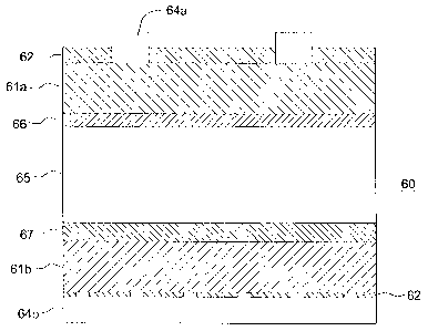
Manufacture." One such cell structure is shown in Fig. 6, which is a partial
cross-
sectional view of a solar cell 60 having n-type front, n-type wafer, p-type
back, and
including a multifunctional transparent, conductive, highly doped silicon
compound
layer 61a requiring a conductive connection to contacts 64a. Layer 61a is an
improvement over other techniques, because the functions of multiple layers
are
combined into a multifunctional layer 61a. This layer can be electrically
passivating,
transparent, and sufficiently conductive for a vertical carrier flow to the
electrodes
(back junction solar cell), may provide the junction with the wafer 65 and/or
may
reduce the reflectance of the incoming light (e.g., antireflection coating).
On the rear
of cell 60, layer 61b can also provide an improvement over other techniques.
Layer
61b may provide the junction with wafer 65, may have a refractive index which
results in a high reflectivity for photons of more than 900 rim wavelength and
may be
sufficiently conductive for vertical carrier flow from the wafer 65 to the
metal
electrode 64b.
[0045] Exemplary layers of cell 60 include the following:
[0046] Layer 61a may be an electrically passivating, transparent and
conductive
film, refractive index in the range of 1.4 < n < 3; thickness in the range of
20 nm
<thickness<110 nm ; specific resistivity in the range of rho < 1000 Ohm cm for
an n-
type wafer; highly doped n-doped 1e18 cm-3<ND<5e21 cm 1. Specific examples
include:
Docket No. 3304.010AWO -11-
CA 02763142 2012-01-05
[0047] n-type amorphous or polycrystalline silicon carbides: phosphorus doped
silicon carbide, nitrogen doped silicon carbide;
[0048] n-type amorphous or polycrystalline silicon: phosphorus doped amorphous
silicon, nitrogen doped amorphous silicon;
[0049] n-type amorphous or poly-crystalline diamond-like-carbon: nitrogen
doped
diamond-like carbon.
[0050] Any of the above examples may include oxygen and hydrogen (n-doped
SiC,Oy.HZ; n-doped SiN,O,,HL).
[0051] Layer 61b may be an electrically passivating and transparent and
conductive film; specific resistivity in the range of rho < 1000 Ohm cm.
Examples
include:
[0052] p-type amorphous or polycrystalline silicon carbides: boron doped
silicon
carbide, aluminum doped silicon carbide, gallium doped silicon carbide;
[0053] p-type amorphous or polycrystalline silicon: boron doped silicon,
aluminum doped silicon, gallium doped silicon;
[0054] p-type amorphous or poly-crystalline diamond-like-carbon: boron doped
diamond-like carbon, aluminum doped diamond-like carbon.
[0055] Any of the above examples may include oxygen and hydrogen (p-doped
SiC,O,,H,; p-doped SiNXOyH,,).
[0056] Layer 65 may be an n-type or p-type crystalline silicon wafer;
thickness is
in the range of w<300 um, base resistivity for n-type wafers 0.5 Ohm cm < rho
< 20
Ohm cm, for p-type wafers 0.1 Ohm cm < rho < 100 Ohm cm.
[0057] Layer 66 may be an electrically passivating interface layer; thickness
<10
nm; no conductivity requirements because of small thickness; no absorption
restrictions due to small thickness. Examples include silicon oxide, silicon
nitride,
intrinsic amorphous silicon, intrinsic polycrystalline silicon, aluminum
oxide,
aluminum nitride, phosphorus nitride, titanium nitride.
Docket No. 3304.010AWO -12-
CA 02763142 2012-01-05
[0058] Layer 67 may be an electrically passivating interface layer; thickness
<10
nm ; no conductivity requirements because of small thickness; no absorption
restrictions due to small thickness. Examples include silicon oxide, silicon
nitride,
intrinsic amorphous silicon, intrinsic polycrystalline silicon, aluminum
oxide,
aluminum nitride, phosphorus nitride, titanium nitride.
[0059] In accordance with the present invention, dielectric layers 62 are
formed
substantially co-planar with contacts (e.g., 64a and 64b), in accordance with
the
partial lift-off principles discussed above with respect to, e.g., Figs. 4A-J
and 5A-E.
[0060] Certain advantages of the present invention lie in the compatibility of
an
"optical" layer to a resist layer when using an underlying, multifunctional
layer that
does not require separate passivation.
[0061] Normally, a dielectric layer (i.e., 42, 52, 62 above) also provides an
electrical passivation function, which requires higher processing
temperatures.
However, if the underlying layer (e.g., 41, 51, 61a, 61b) is a multifunctional
layer
which itself is conductive and passivating, separate passivation by layers 42,
52, 62 is
not required. Therefore, materials 42, 52, 62 can be purely optical and not
substantially passivating, enabling the use of lower processing temperatures,
and also
providing greater process compatibility with the resist layers discussed
herein.
[00621 This Application is related to the commonly-assigned, previously filed
U.S. Provisional Application entitled "High-Efficiency Solar Cell Structures
and
Methods of Manufacture," filed 21 April 2009 and assigned application number
61/171,194; and to commonly-assigned, International Patent Application
entitled
"High-Efficiency Solar Cell Structures and Methods of Manufacture" filed 21
April
2010 and assigned application number PCT/US 10/31869. Each of these
Applications
is again hereby incorporated by reference herein in its entirety. All aspects
of the
present invention may be used in combination with any of the disclosures of
the
above-noted Applications.
[0063] The present invention extends to any type of integrated, semiconductor
circuits having layers requiring conductive contact, in addition to the solar
cell
examples disclosed herein.
Docket No. 3304.010AWO -13-
CA 02763142 2012-01-05
[0064] In summary, certain aspects of the present invention include:
[00651 A method for the fabrication of a metal grid pattern on a substrate in
which
an applied patterned ink or resist film acts as a mask for metal etching and
as a self-
aligned mask for lift-off of a subsequently deposited dielectric;
[00661 A method of patterning a metal grid pattern on a substrate comprising
deposition of a metal film on a surface of the substrate, deposition of an
etch resist on
top of the metal film, etching of the metal film, deposition of a dielectric
on top of the
substrate surface and the resist, and removal of the resist and the overlying
dielectric;
[0067] A structure on a surface on a substrate wherein a metal grid pattern is
surrounded by a dielectric and where no gap exists between the metal and
surrounding
dielectric;
[0068] A method in which a dielectric over a conductive silicon substrate is
only
exposed to resist strippers that preserve the integrity of the dielectric,
thereby
minimizing undesired plating through dielectric defects over the substrate;
[0069] A structure over a surface on a substrate wherein a metal grid pattern
is
surrounded by a dielectric and where no gap exists between the metal and
surrounding
dielectric, resulting in an impenetrable seal between the dielectric and the
metal grid
pattern;
[00701 A structure in which an impenetrable seal between a dielectric over a
substrate and a front grid metal impedes the migration of contaminating metals
into
the substrate; and/or
[0071] A structure and method in which highly conductive metals, which are
also
contaminating, such as copper, are included in the front grid metal stack but
permanently isolated from migration into an underlying silicon substrate.
[0072] In any of the above aspects, the substrate may be a photovoltaic
device; the
metal grid pattern may form the front and/or back contact electrode of a solar
cell; the
metal grid pattern may be subsequently electroplated with metal to improve
electrical
conductivity of the metal grid; the dielectric may be an optical
antireflection layer;
and/or the dielectric may be an optical reflecting layer.
Docket No. 3304.010AWO -14-
CA 02763142 2012-01-05
[0073] The patterned resist may be directly-written and in-situ cured with no
need
for subsequent pattern mask exposure and developing.
[0074] The patterning resist direct-write technique may be ink jetting or
screen-
printing.
[0075] A laser may be used to selectively open holes in the dielectric to
thereby
facilitate the attack of the resist by a resist remover chemical.
[0076] In-situ thermal treatment of the patterned resist and overlying
dielectric
may be used to form holes, cracks or other defects and thereby facilitate the
attack of
the resist by a resist remover chemical, e.g., by a suitable resist solvent,
possibly in
combination with ultrasonic and/or mega-sonic agitation.
[0077] The patterned resist may be "swelled" through exposure to a liquid
which
is absorbed into the patterned resist material, effecting an increase in
volume and area
of the mask material, thereby acting to fracture openings through a brittle
dielectric
coating.
[0078] The dielectric coating may be removed in a pre-defined pattern by
volumetric swelling of the mask material and subsequent lifting of the masking
material along with the dielectric coating layer which encapsulates the mask
material.
[0079] The underlying substrate may be any type of layer requiring conductive
connection, including multifunctional layers.
[0080] Although preferred embodiments have been depicted and described in
detail herein, it will be apparent to those skilled in the relevant art that
various
modifications, additions, substitutions and the like can be made without
departing
from the spirit of the invention and these are therefore considered to be
within the
scope of the invention as defined in the following claims.
Docket No. 3304.010AWO -15-