Note: Descriptions are shown in the official language in which they were submitted.
CA 02763330 2011-11-23
DESCRIPTION
Title of the Invention:
PROCESS FOR PRODUCING SILICON, SILICON, AND PANEL FOR SOLAR
CELLS
Technical Field
[00011
The present invention relates to a process for producing silicon to be used as
a material for fabricating, for example, panels for solar cells.
Background Art
[0002]
High-purity metallic silicon having a resistivity of 0.5-1.5 S2-cm or higher
and a purity of 99.9999% (6 N) or higher is generally used for polysilicon
solar cells.
The most desirable industrial process for producing this high-purity metallic
silicon is a
process in which raw-material metallic silicon that contains impurities in a
large amount
and has a low unit price is refined to remove impurities therefrom and thereby
produce
the high-purity metallic silicon.
[0003]
Among the impurities contained in raw-material metallic silicon, iron,
aluminum, and calcium can be removed by subjecting the molten silicon to
solidification/segregation to thereby cause these impurity metals to remain in
the liquid
phase of the molten silicon. Calcium and the like can be removed by subjecting
the
molten silicon to a vaporization treatment in a vacuum of about 1.3 x 10⁻² to
10' Pa (10-4
to 10-6 Torr), although this method requires much time.
[0004]
However, boron and phosphorus, among the impurities, are exceedingly
difficult to remove. Removal of boron is especially difficult. For example, an
oxidation treatment is being conducted in which the boron is gasified and
removed as a
compound thereof with oxygen or hydrogen, for example, by adding oxygen,
carbon
dioxide, or water vapor to argon as an inert gas and bubbling this mixed gas
into the
molten silicon (patent document 1 and patent document 2).
[0005]
- 1 -
CA 02763330 2011-11-23
The method described above has drawbacks that the operation for oxidizing
the boron (B) contained in raw-material metallic silicon using, for example,
water vapor
and removing the boron as BO gas requires much time, and that silicon
oxidation
simultaneously occurs, resulting in a large loss. Especially when water vapor
is blown
into the molten silicon, a side reaction occurs to evolve hydrogen in a large
amount.
There has hence been a problem concerning safety.
[0006]
There also is a method in which silicon prepared by melting raw-material
metallic silicon is subjected to a vaporization treatment in a vacuum of about
1.3 x 10⁻² to
10"4 Pa (10-4 to 10"6 Torr) in order to remove phosphorus. However, this
method has
had a problem that the treatment requires much time and is costly because the
treatment
is a high-vacuum process. Namely, there has been a problem that the boron and
phosphorus to be removed must be removed by respective separate processes
which are
costly.
[0007]
Meanwhile, as a method for refining silicon using an alkali halide, a
technique has been proposed in which slag is formed from sludge of raw-
material
metallic silicon (the slag includes, as a main component, silicon dioxide
which was
present in the raw-material metallic silicon) and the slag is used for
compositional
regulation during impurity removal to recover the silicon (patent document 3).
However, silicon having an entirely satisfactory purity has not been obtained.
[0008]
Furthermore, patent document 4 describes a step in which 20 g of a
raw-material metallic silicon powder is pulverized and mixed, in a weight
ratio of 1:1,
with NaF having the same particle diameter as the silicon powder, a step in
which the
powder mixture is heated at 1,300 C and the solid silicon is brought into
contact with
the molten NaF, a step in which a second sample is heated at 1,450 C for 10
minutes to
melt the NaF and the raw-material metallic silicon, a step in which these
samples (NaF
and silicon) are cooled to room temperature, and a step in which the silicon
is separated
from the NaF contained in each sample by extraction with an aqueous medium and
by
succeeding decantation and filtration.
- 2 -
CA 02763330 2011-11-23
[0009]
However, the process described in patent document 4 is a mere technique
for silicon refining in which silicon is separated from solid matter
containing NaF and
raw-material metallic silicon by means of filtration, etc. to thereby refine
the silicon.
The process has had problems that the refining effect is insufficient and that
the
operation for separating silicon is not easy.
Prior-Art Documents
Patent Documents
[0010]
Patent Document 1: JP-A-11-49510
Patent Document 2: JP-A-4-228414
Patent Document 3: U.S. Patent No. 4,388,286
Patent Document 4: JP-A-62-502319
Summary of the Invention
Problems that the Invention is to Solve
[0011]
An object of the invention is to eliminate the problems of prior-art
techniques described above and to provide a process for silicon production
with which it
is possible to obtain high-purity metallic silicon from raw-material metallic
silicon by
efficiently and simultaneously removing impurities such as boron (B),
phosphorus (P),
iron (Fe), aluminum (Al), and titanium (Ti) from the raw material in a short
period by
the same process.
Means for Solving the Problems
[0012]
The present invention made various investigations in order to overcome
those problems. As a result, it has been found that by melting raw-material
metallic
silicon and bringing the molten silicon (hereinafter referred to also as
"molten silicon
containing impurity") into contact with a molten salt in a vessel to react the
impurity,
such as boron (B) and phosphorus (P), contained in the molten silicon with the
molten
salt, volatile compounds containing the impurity can be dissolved in the
molten salt or
be vaporized off into the gas phase and the impurity can be thus removed from
the
- 3 -
CA 02763330 2011-11-23
system. The invention has been accomplished based on these findings.
[0013]
Essential points of the invention reside in the following (1) to (16).
(1) A process for producing silicon, which comprises: bringing molten silicon
containing an impurity into contact with molten salt in a vessel to react the
impurity
contained in the molten silicon with the molten salt; and removing the
impurity from the
system.
(2) The process for producing silicon according to (1) above, wherein the step
of
removing the impurity from the system is a step in which a reaction product
obtained by
reacting the impurity contained in the molten silicon with the molten salt is
vaporized
and removed.
(3) The process for producing silicon according to (1) or (2) above, wherein
the step
of removing the impurity from the system is a step in which the impurity
contained in
the molten silicon is removed from the system by evacuation.
(4) The process for producing silicon according to any one of (1) to (3)
above,
wherein the step of removing the impurity from the system is a step in which
the
impurity contained in the molten silicon is removed from the system together
with a
carrier gas.
(5) The process for producing silicon according to any one of (1) to (4)
above,
wherein a lid for controlling the rate of vaporization of the molten salt or
of the reaction
product obtained by reacting the impurity contained in the molten silicon with
the
molten salt is disposed at an inner part or upper part of the vessel.
(6) The process for producing silicon according to any one of (1) to (5)
above,
wherein the reaction between the impurity contained in the molten silicon and
the
molten salt is conducted by forming an interface between the liquid phase of
the molten
silicon and the liquid phase of the molten salt.
(7) The process for producing silicon according to any one of (1) to (6)
above,
wherein the impurity contained in the molten silicon at least includes boron.
(8) The process for producing silicon according to any one of (1) to (7)
above,
wherein the molten salt comprises at least one compound selected from the
group
consisting of halide salts of alkali metals, halide salts of alkaline earth
metals,
- 4 -
CA 02763330 2011-11-23
composite salts containing an alkali metal and a halogen, and composite salts
containing
an alkaline earth metal and a halogen.
(9) The process for producing silicon according to any one of (1) to (8)
above,
wherein the molten salt comprises at least one compound selected from the
group
consisting of sodium fluoride (NaF), sodium silicofluoride (Na2SiF6), cryolite
(Na3A1F6),
mixtures of sodium fluoride and barium fluoride, and mixtures of sodium
fluoride,
barium fluoride, and barium chloride.
(10) The process for producing silicon according to any one of (1) to (9)
above,
wherein the amount of the molten salt is 5-300% by weight based on the molten
silicon.
(11) The process for producing silicon according to any one of (1) to (10)
above,
wherein the impurity contained in the molten silicon are reacted with the
molten salt
while causing the molten silicon to flow by any one of the following methods
(i) to (iv):
(i) a method of blowing an inert gas into the molten silicon,
(ii) a method of inductively stirring the molten silicon by using a
high-frequency induction furnace,
(iii) a method of mechanically forcing the molten salt of an upper layer into
the molten silicon of a lower layer,
(iv) a method of stirring the molten silicon by using a rotor.
(12) The process for producing silicon according to any one of (1) to (11)
above,
wherein the molten salt is continuously added to the molten silicon and the
step of
removing the impurity from the system is conducted by a continuous suction
removal.
(13) The process for producing silicon according to any one of (1) to (12)
above,
wherein after the step of removing the impurity from the system, molten salt
is added to
the molten silicon again and the step is conducted again.
(14) The process for producing silicon according to any one of (1) to (13)
above,
wherein substances removed by the step of removing the impurity from the
system are
recovered to purify molten salt, and the purified molten salt is used again as
molten salt.
(15) Silicon obtained by the process for production according to any one of
(1) to (14)
above, which at least has a boron content of 1.4 ppm or less.
(16) A panel for solar cells, comprising the silicon according to (15) above.
- 5 -
CA 02763330 2011-11-23
Effects of the Invention
[0014]
According to the invention, by bringing molten silicon containing impurity
such as boron (B) and phosphorus (P) into contact with a molten salt in a
vessel, an
interface can be formed between the liquid phase of the molten silicon and the
liquid
phase of the molten salt having a temperature not lower than the melting point
thereof
(hereinafter referred to also as "molten-salt liquid phase") and the impurity
contained in
the molten silicon can be reacted with the molten salt through the interface.
[0015]
By reacting the impurity contained in the molten silicon with the molten salt
through the interface between the molten silicon and the molten salt, the
impurity is
dissolved in the molten salt. Alternatively, by reacting the impurity
contained in the
molten silicon with the molten salt through the interface between the molten
silicon and
the molten salt, reaction products yielded by the reaction are dissolved in
the molten salt
or the reaction products which are compounds having a high vapor pressure
(hereinafter
referred to also as "impurity-containing compounds") are vaporized together
with the
molten salt. Thus, the impurity can be efficiently removed from the molten
silicon.
The impurity-containing compounds dissolved in the molten salt can be removed
from
the system together with the molten salt by vaporizing and removing the molten
salt.
[0016]
In the step of bringing the molten salt into contact with the molten silicon,
the alkali metal or alkaline earth metal which is present in a slight amount
in the molten
salt is incorporated into the molten silicon. However, the alkali metal or
alkaline earth
metal can be easily removed by later processes, e.g., unidirectional
solidification and
vacuum heating.
[0017]
Thus, the process for silicon production of the invention can be used to
efficiently remove impurities such as boron (B) and phosphorus (P) from raw-
material
metallic silicon. According to the process for silicon production of the
invention,
high-purity metallic silicon having a high purity of level 6 N or above can be
rapidly
- 6 -
CA 02763330 2011-11-23
obtained at low cost. The process hence has a high industrial value.
Brief Description of the Drawings
[0018]
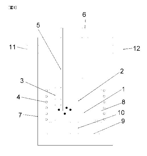
[Fig. 1] Fig. 1 is a diagrammatic sectional view diagrammatically illustrating
one
example of high-purity silicon production apparatus usable in the invention.
[Fig. 2] Fig. 2 is a diagrammatic sectional view diagrammatically illustrating
another
example of high-purity silicon production apparatus usable in the invention.
[Fig. 3] Fig. 3 is a diagrammatic sectional view diagrammatically illustrating
still
another example of high-purity silicon production apparatus usable in the
invention.
[Fig. 4] Fig. 4 is a diagrammatic sectional view diagrammatically illustrating
a further
example of high-purity silicon production apparatus usable in the invention.
[Fig. 5] Fig. 5 is a diagrammatic sectional view diagrammatically illustrating
still a
further example of high-purity silicon production apparatus usable in the
invention.
[Fig. 6] Fig. 6 is a diagrammatic sectional view diagrammatically illustrating
still a
further example of high-purity silicon production apparatus usable in the
invention.
Modes for Carrying Out the Invention
[0019]
Modes for carrying out the invention will be explained below in detail.
The following explanations on constituent elements are for embodiments
(representative
embodiments) of the invention, and the invention should not be construed as
being
limited to the embodiments unless the invention departs from the spirit
thereof
[0020]
The process for silicon production of the invention is characterized by
including steps in which molten silicon obtained by melting raw-material
metallic
silicon containing one or more impurities is brought into contact with molten
salt in a
vessel to react the impurity contained in the molten silicon with the molten
salt and the
impurity is removed from the system (hereinafter referred to also as "removal
step").
[0021]
By bringing molten silicon containing impurity into contact with a molten
salt in a vessel (crucible), an interface can be formed between the liquid
phase of the
molten silicon and the liquid phase of the molten salt and the impurity
contained in the
- 7 -
CA 02763330 2011-11-23
molten silicon can be reacted with the molten salt.
[0022]
By reacting the impurity contained in the molten silicon with the molten salt,
reaction products yielded by the reaction are dissolved in the molten salt or
the reaction
products which are compounds having a high vapor pressure are vaporized
together
with the molten salt. Thus, the impurity can be removed from the molten
silicon.
[0023]
Furthermore, since the molten salt added can also be vaporized and removed,
refined silicon only can be recovered.
[0024]
In the invention, the raw-material metallic silicon is silicon which contains,
for example, boron (B), phosphorus (P), iron (Fe), aluminum (Al), titanium
(Ti), and the
like as impurities.
[0025]
The process of the invention is especially suitable for removing boron (B)
and phosphorus (P) among those impurities.
[0026]
The total concentration of the impurity in the raw-material metallic silicon
is
usually preferably 10-50 ppm, more preferably about 10-30 ppm, by mass. The
lower
the total concentration of the impurity in the raw-material metallic silicon,
the more the
raw material is preferred. However, raw-material metallic silicon containing
impurities in a concentration within that range is a preferred raw material
because this
silicon can be obtained by ordinary arc carbon reduction and hence has a low
cost.
[0027]
The molten salt is not particularly limited so long as the salt is a compound
that melts at the temperature at which the raw-material metallic silicon is
kept molten
and that reacts with impurities contained in the molten silicon, e.g., boron
and
phosphorus, upon formation of an interface between the liquid phase of the
molten
silicon and the liquid phase of the molten salt, thereby enables the impurity
to vaporize
off into the gas phase or dissolve in the molten salt, and is capable of being
vaporized
and removed together with the impurity.
8 -
CA 02763330 2011-11-23
[0028]
Examples of the molten salt include: halide salts of alkali metals, such as
sodium fluoride (NaF), potassium fluoride (KF), sodium chloride (NaC1), and
potassium
chloride (KC1); halide salts of alkaline earth metals, such as calcium
fluoride (CaF2),
barium fluoride (BaF2), calcium chloride (CaCl2), and barium chloride (BaC12);
composite salts containing an alkali metal and a halogen, such as sodium
silicofluoride
(Na2SiF6), cryolite (Na3A1F6), chiolite (Na5Al3F14), KA1Cl4, and NaA1C14; and
composite salts containing an alkaline earth metal and a halogen, such as
BaCaCl4 and
MgCaF4. Preferred of these are the salts which contain fluorine as the
halogen.
[0029].
Among those salts, sodium silicofluoride (Na2SiF6) is a composite salt of
sodium fluoride (NaF) and silicon fluoride (SiF4), while cryolite (Na3A1F6) is
a
composite salt of sodium fluoride (NaF) and aluminum fluoride (A1F3).
[0030]
Suitable examples among those include sodium fluoride (NaF), sodium
silicofluoride (Na2SiF6), cryolite (Na3A1F6).mixtures of sodium fluoride and
barium
fluoride, and mixtures of sodium fluoride, barium fluoride, and barium
chloride.
[0031]
In particular, sodium silicofluoride (Na2SiF6) decomposes to generate SiF4
(gas) and react with the impurity, and this results in no silicon loss.
Consequently,
sodium silicofluoride (Na2SiF6) is especially preferred.
[0032]
Suitable examples further include potassium fluoride (KF), potassium
cryolite (K3A1F6), and a compound of potassium fluoride and calcium fluoride
(molar
ratio, 1:1).
[0033]
In general, the cryolite (Na3A1F6) for use in electrolytic refining of
aluminum is easily available at low cost and is easy to use industrially.
[0034]
In the case where the liquid phase of a molten salt is to be formed over the
liquid phase of molten silicon, it is preferred to use a molten salt having a
lower density
- 9 -
CA 02763330 2011-11-23
than silicon (Si). Examples of this molten salt include the halide salts of
alkali metals.
[0035]
In the case where the liquid phase of a molten salt is to be formed under the
liquid phase of molten silicon, it is preferred to use a molten salt having a
higher density
than silicon. Examples of this molten salt include the halide salts of
alkaline earth
metals.
[0036]
It is desirable that the molten salt should have a lower impurity content.
However, the impurity also has been halogenated in many cases and mostly
vaporize at
the treatment temperature. The impurity hence poses no problem. It is
therefore
possible to use an ordinary industrial chemical as the molten salt.
[0037]
In the case where a mixture of sodium fluoride and one or more other
molten salts is used as molten salts, the amount of the sodium fluoride to be
used, based
on the amount (total amount) of the other molten salts, is usually preferably
5% by
weight or more, more preferably 10% by weight or more, especially preferably
20% by
weight or more, and is usually preferably 300% by weight or less, more
preferably
100% by weight or less, especially preferably 50% by weight or less.
[0038]
The amount of the molten salt to be used, based on the starting-material
metallic silicon, is usually preferably 5% by weight or more, more preferably
10% by
weight or more, even more preferably 20% by weight or more, especially
preferably
30% by weight or more, and is usually preferably 300% by weight or less, more
preferably 100% by weight or less, especially preferably 50% by weight or
less.
[0039]
By regulating the amount of the molten salt to 5% by weight or more, a
sufficient refining effect is obtained. By regulating the amount of the molten
salt to
300% by weight or less, the molten salt can be prevented from reacting also
with the
silicon (Si) and thereby lowering the yield of silicon (Si).
[0040]
Raw-material metallic silicon and a salt to be melted may be mixed with
- 10 -
CA 02763330 2011-11-23
each other and then simultaneously heated and melted. Alternatively, use may
be
made of a method in which raw-material metallic silicon only is heated and
melted
before a salt to be melted is added thereto. Furthermore, it is possible to
use fluxed
salts prepared by optionally mixing salts to be melted, heating and melting
the salts, and
then cooling the melt.
[0041]
The temperature at which raw-material metallic silicon and a salt to be
melted are heated and melted preferably is not lower than the melting point of
silicon
(1,410 C), and is more preferably 1,450 C or higher. The upper limit of the
temperature is usually preferably 2.400 C or lower, more preferably 2,000 C or
lower.
[0042]
Thus, the molten silicon obtained by melting raw-material metallic silicon is
brought into contact with a molten salt, and an interface can be thereby
formed between
the liquid phase of the molten silicon and the liquid phase of the molten
salt.
[0043]
Impurities contained in the molten silicon can be reacted with the molten
salt through the interface between the liquid phase of the molten silicon and
the liquid
phase of the molten salt. As a result, the impurity can be vaporized off into
the gas
phase or moved to the molten salt.
[0044]
Furthermore, the gas formed by vaporization of the molten salt, the gas of a
decomposition product formed by partial decomposition of a composite compound,
or
the like can be caused to act on the molten silicon through the interface
between the
liquid phase of the molten silicon and the liquid phase of the molten salt.
Impurities
contained in the molten silicon can be thereby reacted with the molten salt.
[0045]
The reaction time, i.e., the period of contact between the molten silicon and
molten salt, is usually preferably 0.1 hour or longer, more preferably 0.25
hours or
longer, especially preferably 0.5 hours or longer, and is usually preferably 3
hours or
shorter, more preferably 2 hours or shorter, even more preferably 1 hour or
shorter.
[0046]
- 11 -
CA 02763330 2011-11-23
The longer the reaction time, the higher the effect of diminishing the
impurity. However, shorter reaction times are desirable from the standpoint of
process
cost.
[0047]
It is preferred that the impurity-containing compounds yielded by forming
the interface as described above, i.e., reaction products formed by reacting
impurities
contained in the molten silicon with the molten salt, should be removed by
vaporizing
the compounds together with the molten salt (removal by vaporization).
[0048]
The pressure (degree of vacuum) during the removal by vaporization is
usually preferably atmospheric pressure. In some cases, it is preferred to
reduce the
pressure to about 10"4 Pa. When the specific gravity of the molten salt is
smaller than
the specific gravity of the molten silicon and the liquid phase of the molten
salt has been
formed over the liquid phase of the molten silicon, then it is generally
preferred that the
pressure should be atmospheric pressure.
[0049]
It is preferred that during the removal by vaporization, an inert gas such as
argon should be passed as a carrier gas through the vessel, because the
removal by
vaporization is accelerated thereby.
[0050]
Use may be made of a method in which the molten-salt liquid phase
containing impurities that overlies the molten-silicon liquid phase is partly
removed
mechanically and the removal by vaporization is restarted thereafter, in order
to
accelerate the removal by vaporization.
[0051]
In the case where the impurity concentration of the molten silicon has
decreased to a desired value as a result of the impurity removal by reacting
the impurity
contained in the molten silicon with the molten salt, the silicon only may be
recovered
from a middle part or the bottom of the vessel.
[0052]
Use may also be made of a method in which the vessel containing the
- 12 -
CA 02763330 2011-11-23
molten silicon and molten salt that have been melted by heating is tilted to
transfer the
contents to another vessel and this vessel is allowed to stand. As a result,
the molten
silicon and the molten salt separate into respective two phases. Consequently,
the two
phases in this state are cooled and solidified, and the silicon is then
recovered. In this
case, when the recovered silicon contains the molten salt, it is preferred
that the molten
salt is removed by vaporization later.
[0053]
When the specific gravity of the molten salt is larger than the specific
gravity of silicon and the liquid phase of the molten salt has been formed
under the
liquid phase of the molten silicon, the reaction may be conducted in the
following
manner. Since the halide salt of an alkaline earth metal, which has a large
specific
gravity, has a low vapor pressure, this molten salt is vaporized by reducing
the pressure
to about 100 Pa and the molten silicon can be bubbled therewith. Thus, the
reaction
can be accelerated.
[0054]
It is preferred that the temperature of the molten-silicon liquid phase and
molten-salt liquid phase during the vacuum removal should be in the same range
as the
temperature at which raw-material metallic silicon and a salt to be melted are
heated
and melted.
[0055]
By forming a flow of the molten silicon at the interface between the
molten-silicon liquid phase and the molten-salt liquid phase, for example, by
any one
method selected from the following (i) to (vi), not only the reaction between
the
impurity and the molten salt can be accelerated but also compounds of the
impurity,
which are products of the reaction between the impurity and the molten salt,
can be
more efficiently removed.
[0056]
To form a flow of the molten silicon preferably means to reduce the relative
thickness of the boundary layer, which functions as a reaction field formed in
the
vicinity of the interface between the molten-silicon liquid phase and the
molten-salt
liquid phase. By forming the flow, the reaction between the impurity and the
molten
,0
CA 02763330 2011-11-23
salt can be more efficiently accelerated.
[0057]
(i) A method in which an inert gas is blown into the molten-silicon liquid
phase.
[0058]
(ii) A method in which a high-frequency induction furnace is used to
inductively stir the
molten-silicon liquid phase.
[0059]
(iii) A method in which the molten salt of an upper layer is mechanically
forced into the
molten-silicon layer of a lower layer. The term "the molten salt is
mechanically forced
into the molten-silicon layer" means that a mechanical means, e.g., a concave
jig made
of graphite, is used to force the overlying molten salt into the underlying
molten-silicon
layer.
[0060]
(iv) A method in which a rotor is used to stir the liquid phase.
[0061]
(v) A method in which a powder of the molten salt is blown into the molten-
silicon
liquid phase together with an inert gas.
[0062]
(vi) A method in which in a configuration including molten silicon as a lower
layer and
a molten salt as an upper layer, the surface of the molten silicon is caused,
by inductive
stirring, to flow radially from the center of the vessel toward the periphery
thereof and
the surface-layer part of the molten salt is caused, by means of a rotating
plate, to flow
radially from the center of the vessel toward the periphery thereof. According
to this
method, the part of the molten salt which is present at the boundary between
the molten
silicon and the molten salt can be caused to flow from the periphery of the
vessel
toward the center thereof, and the molten-silicon liquid phase and the molten-
salt liquid
phase can be caused to flow in opposite directions at the interface
therebetween.
[0063]
After the impurity has been removed by vaporization together with the
molten salt, the vessel may be evacuated according to need to thereby remove
the
residual molten salt, before the molten silicon is solidified. Thus, high-
purity silicon
- 14 -
CA 02763330 2011-11-23
can be obtained. Use may also be made of a method in which when the molten
silicon
is solidified, so-called unidirectional solidification is conducted to remove
the residual
molten salt and impurities by segregation. Thus, silicon having a higher
purity can be
obtained.
[0064]
After the impurity has been removed by any of those methods, the silicon
may be further subjected to removal of alkali metals and alkaline earth metals
therefrom.
Thus, silicon having an even higher purity can be obtained.
[0065]
The removal of alkali metals and alkaline earth metals can be conducted by
a common method which itself is known. Examples thereof include: a
unidirectional
solidification method; a method in which either an inert carrier gas or a gas
obtained by
adding oxygen, carbon dioxide, or water vapor to an inert carrier gas is
brought into
contact with the surface of the molten-silicon liquid phase; a method in which
the gas is
blown into the molten-silicon liquid phase; and a method in which the alkali
metals and
the alkaline earth metals are vaporized and removed under high vacuum.
[0066]
As the carrier gas, use can be made of an inert gas such as, for example,
argon. However, the carrier gas should not be construed as being limited to
argon, so
long as the desired silicon is obtained.
[0067]
The process of the invention can be carried out using a silicon refining
apparatus which includes a vessel for melting therein raw-material metallic
silicon and a
salt to be melted and in which the vessel can be filled with an inert gas
atmosphere, e.g.,
argon, while being kept in a reduced-pressure state or atmospheric-pressure
state.
[0068]
It is preferred that the apparatus for use in the process for high-purity
silicon
production of the invention should include: a vessel which can be brought into
a
high-vacuum state and can also be closely filled with an inert gas atmosphere,
e.g.,
argon; a crucible disposed in the vessel; a coil for heating the crucible by
high-frequency heating or a heater which is capable of heating the crucible by
resistance
- 15 -
CA 02763330 2011-11-23
heating; and a power supply for these.
[0069]
It is also preferred that the apparatus should further include: a device for
stirring the contents of the crucible with a graphite blade or for blowing
argon gas into
the molten silicon; and a device for introducing a salt to be melted, raw-
material
metallic silicon, etc.
[0070]
In the case where vaporization of the molten salt will occur in a large
amount, it is preferred to suitably dispose a bag filter or the like for
trapping the vapor.
[0071]
In the case where the molten salt used has a high vapor pressure, it is
preferred to dispose an inner lid within the vessel or dispose a lid at the
opening of the
vessel to thereby inhibit vaporization of the molten salt, prolong the period
of reaction
with the molten silicon, and reduce the amount of the molten salt to be used.
[0072]
Embodiments of the process of the invention will be explained below in
detail together with the effects thereof, etc.
[0073]
(a) With respect to the case where sodium fluoride (NaF) is used as molten
salt:
Sodium fluoride (NaF) has a specific gravity at 1,500 C of about 1.8, which
is smaller than the specific gravity of about 2.6 for molten silicon.
Consequently, in
the crucible, an interface is formed between the molten-silicon liquid phase
as a lower
layer and the NaF liquid phase as an upper layer.
[0074]
It is thought that the following reaction occurs through the interface. The
boron (B) contained as an impurity in the molten silicon is converted to the
reaction
product, which, when generated in a slight amount, moves into and dissolves in
the
molten salt or vaporizes off into the gas phase.
4NaF + B = 3Na + NaBF4 or 3NaF + B = 3Na + BF3
[0075]
With respect to the aluminum (Al) contained as an impurity in the molten
- 16 -
CA 02763330 2011-11-23
silicon also, it is thought that the following reaction occurs. As in the case
of the
boron, the reaction product moves into the molten salt or vaporizes off into
the gas
phase.
Al + 6NaF = Na3A1F6 + 3Na
[0076]
For causing the reactions to proceed rapidly, it is important to rapidly
remove the products of the reactions. It is preferred that the removal of the
reaction
products should be conducted by sucking the reaction products from the
crucible
together with a carrier gas, e.g., argon, to thereby remove the reaction
products from the
system.
[0077]
For example, it is preferred to use a method in which a molten salt is
suitably continuously added to molten silicon and the products of the
reactions are
removed by continuous suction. By using this method, the amount of the molten
salt
to be use can be minimized and the refining can be carried out in a short
period.
[0078]
After the removal step, a molten salt may be added again to conduct a
removal step again. Thus, the purity of the silicon can be improved.
[0079]
The molten salt removed in the removal step can be recovered, purified by a
known method, and then reused as a molten salt.
[0080]
Details of reactions of phosphorus (P) as an impurity are unclear. It is,
however, thought that a fluoride or composite fluoride of phosphorus (P)
generates at
the interface and this reaction product shows the same behavior as the boron
(B).
[0081]
Through those reactions, the metallic sodium is incorporated into the molten
silicon. However, the metallic sodium mostly vaporizes off during the process.
[0082]
The NaBF4, BF3, and the like are thought to first dissolve in the NaF.
However, these compounds also have a high vapor pressure and mostly vaporize
off
- 17 -
CA 02763330 2011-11-23
during the process. Even if such impurities remain dissolved in the NaF, these
impurities can be removed together with the NaF as the molten salt in the
latter half of
the process by vaporizing the NaF at an elevated temperature or under vacuum.
[0083]
Other impurities including phosphorus (P), iron (Fe), aluminum (Al), and
titanium (Ti) also are removed from the molten silicon by the same process.
[0084]
There is a possibility that the NaF might react with the Si to yield SiF4 and
the gaseous SiF4 might react with impurities. In any case, the impurity can be
removed as fluoride compounds having a high vapor pressure.
[0085]
(b) With respect to the case where composite compound of NaF and SiF4
(Na2SiF6) is
used as molten salt:
It is also possible to use, for example, a composite compound of NaF and
SiF4 (Na2SiF6) from the beginning. In this case, the Na2SiF6, before becoming
a liquid
phase, partly decomposes into NaF and SiF4.
[0086]
Since SiF4 is a gas, it is favorable to mechanically force the Na2SiF6 into
the
Si melt because the gas reacts with impurities contained in the melt. There
also is an
advantage that the NaF is inhibited from reacting with the molten-silicon
liquid phase
(Si) and, hence, the yield of refined silicon is improved.
[0087]
(c) With respect to the case where salt mixture of NaF and BaF2 is used as
molten salts:
Furthermore, it is possible to use, for example, a salt mixture of NaF and
BaF2 as molten salts and dispose these molten salts under molten silicon. So
long as
the NaF/BaF2 salt mixture has a BaF2 content of 40% by mole or higher, this
salt
mixture has a higher specific gravity than liquid silicon, which has a
specific gravity of
about 2.6, and sinks beneath the liquid silicon. It is thought that when the
pressure of
the atmosphere in the system in this state is reduced, the NaF itself
vaporizes and the
gas can be bubbled into the liquid silicon to accelerate the reactions.
[0088]
- 18 -
CA 02763330 2011-11-23
It is preferred that those reactions should be conducted usually at 0.5-2 atm.
In the case where the molten salts are to be removed completely, it is
preferred to
vaporize the molten salts at a vacuum of about 130 to 13 X 10 3 Pa (1 to 10-'
Torr). As a
result, the silicon remains as the only melt, and it becomes possible to
easily recover the
silicon by pouring the silicon into a casting mold.
[0089]
Next, modes suitable for carrying out the invention are explained on the
basis of the production apparatus shown in the drawings.
[0090]
Fig. 1 is a sectional view diagrammatically illustrating one example of
high-purity metallic silicon production apparatus usable in the invention.
This
apparatus is configured of a closable chamber 7, a crucible 3 disposed inside
the
chamber, a coil 4 for induction heating, a heat insulator 8, a support 10 for
the crucible,
a casting mold 9 for silicon casting, etc. Raw-material metallic silicon I and
a molten
salt 2 are placed in the crucible 3 in the state of having been separated into
respective
liquid phases.
[0091]
The closable chamber 7 has, attached thereto, a gas introduction port 11, a
gas discharge port 12, a feed material charging port 6, etc., and the internal
pressure of
the chamber 7 can be regulated in the range of about 0.01 to 2x10⁵ Pa (from
vacuum to
2 atm).
[0092]
The induction coil 4 for heating, the heat insulator 8, and the crucible 3
have
been configured so as to be capable of being tilted in an integrated manner.
The
raw-material metallic silicon 1 which has undergone the treatment is poured
into the
casting mold 9.
[0093]
In this apparatus, to stir the interface between the two liquid phases is
advantageous for the impurity treatment. By blowing an inert gas, e.g., argon,
into the
liquid phases through a pipe 5, the liquid phases can be stirred and the state
of contact at
the interface between the two liquid phases can be improved.
- 19 -
CA 02763330 2011-11-23
[0094]
Fig. 2 is a sectional view diagrammatically illustrating another example of
high-purity silicon production apparatus usable in the invention. In Fig. 2, a
technique
for stirring the liquid phases using a stirring plate 13 is described in place
of gas
blowing. However, the other parts are substantially the same as in Fig. 1.
[0095]
Fig. 3 is a sectional view diagrammatically illustrating still another example
of high-purity silicon production apparatus usable in the invention. In Fig.
3, a
technique for inductively stirring the liquid phase of silicon using a high-
frequency
induction furnace is described in place of gas blowing. However, the other
parts are
substantially the same as in Fig. 1.
[0096]
In the case of induction heating, use of a power supply having a relatively
low frequency, e.g., about 1-5 kHz, is desirable because an induced current
occurs
within the silicon melt and this results in a peculiar stirring phenomenon. In
particular,
since the silicon melt can be stirred without requiring insertion of a
stirring plate or the
like into the melt, that technique is preferred also from the standpoint of
contamination.
[0097]
Fig. 4 is a sectional view diagrammatically illustrating a further example of
high-purity silicon production apparatus usable in the invention. In Fig. 4,
in place of
gas blowing, a technique is described in which a concave jig 13 made of
graphite is
used to mechanically force the molten salt as an upper layer into the molten
silicon layer
as a lower layer to stir the molten silicon layer by means of the gas evolved
by
vaporization of the molten salt. However, the other parts are substantially
the same as
in Fig. 1.
[0098]
Fig. 5 is a sectional view diagrammatically illustrating still a further
example of high-purity silicon production apparatus usable in the invention.
In Fig. 5,
an embodiment is described in which a molten salt 2 which has a large specific
gravity
underlies the molten silicon obtained by melting starting-material metallic
silicon 1.
However, the other parts are substantially the same as in any of Figs. 1 to 4.
- 20 -
CA 02763330 2011-11-23
[0099]
Fig. 6 is a sectional view diagrammatically illustrating still a further
example of high-purity silicon production apparatus usable in the invention.
In Fig. 6,
a powdery or granular salt to be melted is continuously introduced through the
feed
material charging port 6 and placed on the surface of the molten silicon.
Vaporized
substances also are continuously discharged from the system through a suction
port 14.
The other parts are substantially the same as in any of Figs. 1 to 5.
[0100]
In Figs. 1 to 5. a device for trapping the molten salt and reaction products
which have been vaporized, such as, for example, a cyclone, filter, or
evacuator (each
being not shown), is disposed ahead of the gas discharge port 12 or suction
port 14.
[0101]
A high-frequency current of one to tens of kilohertz is usually supplied to
the heating coil 4 from a power supply (not shown) to generate an induced
current in the
graphite crucible 3 or in the molten silicon and thereby heat and melt the
contents and
inductively stir the contents.
[0102]
The molten salt trapped by the cyclone usually contains impurities such as
boron and phosphorus in a large amount. Consequently, for reclaiming the
trapped salt
as a starting material, it is preferred to wash the salt with, for example,
pure water and
dry the salt, or it is preferred to heat the salt to a temperature lower than
the melting
point thereof or melt the salt, under vacuum. Thus, the trapped salt can be
easily
purified because compounds containing impurities such as boron and phosphorus
generally are water-soluble and have a high vapor pressure.
[0103]
The operation explained above is repeated according to need. As a result,
silicon having a boron content of 1 ppm or less and a phosphorus content of 1
ppm or
less can be obtained. As stated above, alkali metals and alkaline earth metals
are
removed from this silicon according to need. Thus, silicon having a higher
purity can
be obtained.
[0104]
- 21 -
CA 02763330 2011-11-23
The silicon obtained by the process of the invention may have the following
impurity concentrations. The concentration of boron (B) therein is usually
preferably
1.6 ppm or less, more preferably 1.4 ppm or less, even more preferably 0.38
ppm or less,
especially preferably 0.2 ppm or less.
[0105]
The concentration of phosphorus (P), among the impurity concentrations of
the silicon obtained by the process of the invention, is usually preferably 22
ppm or less,
more preferably 11 ppm or less, even more preferably 5.4 ppm or less,
especially
preferably 4 ppm or less.
[0106]
The concentration of iron (Fe), among the impurity concentrations of the
silicon obtained by the process of the invention, is usually preferably 1,300
ppm or less,
more preferably 88 ppm or less, even more preferably 37 ppm or less,
especially
preferably 15 ppm or less.
[0107]
The concentration of titanium (Ti), among the impurity concentrations of
the silicon obtained by the process of the invention, is usually preferably 22
ppm or less,
more preferably 15 ppm or less, even more preferably 13 ppm or less,
especially
preferably 3 ppm or less.
[0108]
The concentration of aluminum (Al), among the impurity concentrations of
the silicon obtained by the process of the invention, is usually preferably 20
ppm or less,
more preferably 18 ppm or less, even more preferably 2 ppm or less, especially
preferably I ppm or less.
[0109]
The concentration of calcium (Ca), among the impurity concentrations of
the silicon obtained by the process of the invention, is usually preferably 22
ppm or less,
more preferably 2.1 ppm or less, even more preferably 1.2 ppm or less,
especially
preferably 15 ppm or less.
[0110]
The concentrations of impurities in silicon can be determined through
- 22 -
CA 02763330 2011-11-23
analysis with, for example, an ICP-MS (inductively coupled plasma mass
spectrometer).
[0111]
The purity of the silicon obtained by the process of the invention may be
further heightened by using other refining method(s) in combination with the
process of
the invention. The silicon obtained may be processed by a known method to
thereby
obtain a silicon ingot or silicon wafer for solar cells.
[0112]
The process of the invention is especially suitable for use as a process for
industrially producing high-purity silicon to be used, for example, as a
material for
producing panels for solar cells.
Examples
[0113]
The invention will be explained below in more detail by reference to
Examples. However, the invention should not be construed as being limited to
the
following Examples unless the invention departs from the spirit thereof.
[0114]
In the following Examples, the impurity concentrations (ppm) in silicon are
values (on weight basis) obtained through analysis with an ICP-MS (inductively
coupled plasma mass spectrometer).
[0115]
The raw-material metallic silicon used in the Examples had the following
impurity concentrations: boron (B), 1.6 ppm; phosphorus (P), 30 ppm; iron
(Fe), 95
ppm; titanium (Ti), 25 ppm; aluminum (Al), 500 ppm; calcium (Ca), 19 ppm;
sodium
(Na), below detection limit.
[0116]
EXAMPLE 1
The chamber 7 shown in Fig. 1 was filled with an argon gas atmosphere
having a pressure of 1 atm. Raw-material metallic silicon to be refined and a
salt
(NaF) to be melted were placed in the graphite crucible 3 in amounts of 250 g
and 50 g,
respectively. The silicon and the salt were heated to about 1,550 C and
allowed to
stand still for about 2 hours.
- 23 -
CA 02763330 2011-11-23
[0117]
Thereafter, the chamber 7 was evacuated to 1.3x 10-' to 1.3 x 10⁻³ Pa
(10-3-10-5 Torr) to completely vaporize the NaF. The crucible 3 was tilted to
pour the
residual silicon into the casting mold 9, and the silicon was solidified.
[0118]
The concentrations of major impurities in the silicon obtained were as
follows: boron (B), 1.4 ppm; phosphorus (P), 22 ppm; sodium (Na), 1 ppm. Both
the
concentrations of boron and phosphorus had decreased, and the concentration of
sodium
also was sufficiently low.
[0119]
EXAMPLE 2
The chamber 7 shown in Fig. 5 was filled with an argon gas atmosphere
having a pressure of 1 atm. In the crucible 3 made of graphite were placed 250
g of
raw-material metallic silicon to be refined and salts to be melted (NaF +
BaF2: 30 g + 30
g). The silicon and the salts were heated to about 1,550 C and allowed to
stand still
for about 2 hours. In this case, the molten salts had a larger specific
gravity and, hence,
the molten silicon was in the state of floating on the molten salts.
[0120]
Thereafter, the internal pressure of the chamber was reduced to 1.3 x 10³ Pa
(10 Torr). When the system is in this state, a gas is evolved just in the
vicinity of the
interface between the molten silicon and the molten salts and the evolved gas
causes
bubbling to satisfactorily stir the interface between the molten silicon and
the molten
salts. The system in this state was allowed to stand for about two hours and
poured
into the casting mold 9, in which the molten silicon and the molten salts were
allowed to
separate from each other and solidify.
[0121]
The concentrations of major impurities in the silicon obtained were as
follows: boron (B), 1.6 ppm; phosphorus (P), 11 ppm. The concentration of
phosphorus had decreased to about 1/3 the original concentration thereof in
the
raw-material metallic silicon, whereas the concentration of boron remained
unchanged.
The BaF2 used as a molten salt was analyzed and, as a result, boron was
detected in an
- 24 -
CA 02763330 2011-11-23
amount of 3.3 ppm. This was thought to be the cause of the unchanged boron
concentration.
[0122]
EXAMPLE 3
The chamber 7 shown in Fig. 5 was filled with an argon gas atmosphere
having a pressure of 1 atm. In the crucible 3 made of graphite were placed 250
g of
raw-material metallic silicon to be refined and salts to be melted (NaF + BaF2
+ BaC12:
30 g + 30 g + 10 g). The silicon and the salts were heated to about 1,550 C
and
allowed to stand still for about 2 hours.. In this case, as in Example 2, the
molten salts
had a larger specific gravity and, hence, the molten silicon was in the state
of floating
on the molten salts.
[0123]
Thereafter, the internal pressure of the chamber was reduced to 1.3 x 10³ Pa
(10 Torr). When the system is in this state, a gas is evolved just in the
vicinity of the
interface between the silicon and the molten salts and the evolved gas causes
bubbling
to satisfactorily stir the interface between the molten silicon and the molten
salts. The
system in this state was allowed to stand for about two hours and poured into
the casting
mold 9, in which the silicon and the molten salts were allowed to separate
from each
other and solidify.
[0124]
The concentrations of major impurities in the silicon obtained were as
follows: boron (B), 1.4 ppm; phosphorus (P), 19 ppm; iron (Fe), 37 ppm;
titanium (Ti),
15 ppm; aluminum (Al), 18 ppm; calcium (Ca), 22 ppm.
[0125]
As shown above, the concentration of phosphorus had decreased to about
2/3 the original concentration thereof in the raw-material metallic silicon.
With
respect to boron, the purity in terms of concentration thereof had increased
from 1.6
ppm to 1.4 ppm, although the BaF2 used as a molten salt contained boron in an
amount
of 3.3 ppm. With respect to aluminum, the purity in terms of concentration
thereof
had greatly increased from 500 ppm to 18 ppm. With respect to impurities such
as
iron, titanium, and the like also, the purity in terms of concentration
thereof had
- 25 -
CA 02763330 2011-11-23
increased.
[0126]
EXAMPLE 4
The chamber 7 shown in Fig. 1 was filled with an argon gas atmosphere
having a pressure of 1 atm. Raw-material metallic silicon to be refined and a
salt
(NaF) to be melted were placed in the graphite crucible 3 in amounts of 250 g
and 50 g,
respectively. The silicon and the salt were heated to about 1,550 C.
Furthermore,
argon gas was blown into the liquid phase of silicon to stir the contents for
about 1 hour.
Thereafter, the chamber 7 was evacuated to 1.3X101 to 10-3 Pa (10-3-10-' Torr)
to
completely vaporize the NaF.
[0127]
Thereafter, 50 g of NaF was introduced again into the crucible to form an
interface between the NaF and silicon liquid phases. An argon gas was blown
into the
silicon liquid phase to stir the contents for about 1 hour, and the chamber
was thereafter
evacuated in the same manner to completely vaporize the NaF. The crucible was
tilted
to pour the residual silicon into the casting mold 9, and the silicon was
solidified.
[0128]
The concentrations of major impurities in the silicon obtained were as
follows: boron (B), 0.37 ppm; phosphorus (P), 4 ppm; iron (Fe), 88 ppm;
titanium (Ti),
22 ppm; aluminum (Al), 20 ppm; calcium (Ca), 21 ppm.
[0129]
As shown above, the purities in terms of boron concentration and
phosphorus concentration greatly increased from 1.6 ppm to 0.37 ppm and from
30 ppm
to 4 ppm, respectively.
[0130]
EXAMPLE 5
The chamber 7 shown in Fig. 6 was filled with an argon gas atmosphere
having a pressure of 1 atm. Raw-material metallic silicon to be refined was
placed in
the graphite crucible 3 in an amount of 6.1 kg. The silicon was heated to
about
1,550 C.
[0131]
- 26 -
CA 02763330 2011-11-23
The concentrations of major impurities in the silicon used in this Example
were as follows: boron (B), 1.9 ppm; phosphorus (P), 4.6 ppm; iron (Fe), 1,500
ppm;
titanium (Ti), 11 ppm; aluminum (Al), 280 ppm; calcium (Ca), 19 ppm.
[0132]
Furthermore, granular NaF was continuously introduced little by little
through the feed material charging port and added to the surface of the molten
silicon.
The rate of addition was regulated to I kg/hr. The impurity-containing NaF
which had
vaporized from the surface of the silicon was sucked and discharged outside
together
with argon gas as a carrier gas through a suction tube. A cyclone was disposed
ahead
of the suction tube, and the vaporized substances were recovered therewith.
[0133]
About 6 kg of NaF was added in the manner described above. Thereafter,
at the time when vaporization of the NaF had substantially ended, the chamber
7 was
evacuated to 1.3 x 10"1 to 10-3 Pa (10"3-10-5 Torr) to completely vaporize the
NaF.
Thereafter, the crucible was tilted to pour the residual silicon into the
casting mold 9,
and the silicon was solidified.
[0134]
The concentrations of major impurities in the silicon obtained were as
follows: boron (B), 0.38 ppm; phosphorus (P), 5.4 ppm; iron (Fe), 1,300 ppm;
titanium
(Ti), 13 ppm; aluminum (Al), I ppm; calcium (Ca), 1.2 ppm.
[0135]
As shown above, the purities in terms of boron concentration and aluminum
concentration greatly increased from 1.9 ppm to 0.38 ppm and from 280 ppm to 1
ppm,
respectively.
[0136]
The concentrations of impurities in the NaF used in this Example were as
follows: boron (B), 0.9 ppm; phosphorus (P), 1.2 ppm. In the compounds of NaF
which were recovered from the cyclone after the experiment, high-concentration
impurities which were 11 ppm boron (B) and 9 ppm phosphorus (P) were detected.
[0137]
Furthermore, the recovered compounds of NaF were melted at about
- 27 -
CA 02763330 2011-11-23
1,050 C in a graphite crucible, treated for about 1 hour in an argon
atmosphere of 0.1
atm, and then cooled and solidified. The resultant sample was analyzed for
impurities.
As a result, the impurity concentrations had greatly decreased to 0.5 ppm for
boron (B)
and 0.6 ppm for phosphorus (P). Thus, purified NaF having a high purity which
rendered the NaF reusable was able to be obtained.
[0138]
While the invention has been described in detail and with reference to
specific embodiments thereof, it will be apparent to one skilled in the art
that various
changes and modifications can be made therein without departing from the
spirit and
scope thereof. This application is based on a Japanese patent application
filed on July
3, 2009 (Application No. 2009-159003), the entire contents thereof being
incorporated
herein by reference.
Industrial Applicability
[0139]
The process of the invention is especially suitable for use as a process for
industrially producing high-purity silicon to be used, for example, as a
material for
producing panels for solar cells.
Description of the Reference Numerals
[0140]
1 Raw-material metallic silicon
2 Molten salt
3 Crucible
4 Coil for induction heating
Pipe
6 Feed material charging port
7 Chamber
8 Heat insulator
9 Casting mold
Support for crucible
11 Gas introduction port
12 Gas discharge port
28 -
CA 02763330 2011-11-23
13 Stirring plate/concave jig
14 Suction port for gases of molten salt and reaction products
- 29 -