Note: Descriptions are shown in the official language in which they were submitted.
CA 02763444 2011-11-24
WO 2010/145019 PCT/CA2010/000919
DUAL SWITCHING FREQUENCY HYBRID iPOWER CONVERTER
CROSS REFERENCE TQ RELATED? APPLICATIONS
This application claims priority of US Patent Application having serial number
611187,170 which was filed on June 15, 2009 abd entitled "DUAL SWITCHING
FREQUENCY HYBRID POWER CONVERTER", the specification of which is hereby
incorporated by reference.
This application also claims priority of US Patent Application having serial
number 61/233,664 which was filed on August 13õ 2009 and entitled 'ENERGY
STORAGE SYSTEM AND METHOD', the specification of which is hereby incorporated
by reference.
The present application also relates to PCT Application entitled "ENERGY
STORAGE SYSTEM AND METHOD" file on June 15, 2010, by the same Applicant, the
specification of which is incorporated herein by reference.
FIELD OF THE INVENTION
The invention relates to electric converters for AC to DC and DC to AC voltage
conversion for mono-phase or multi-phase systems, and more particularly
concerns a dual switching frequency hybrid power converter enabling to reduce
conduction and commutation tosses.
BACKGROUND OF THE INVENTION
With the rising costs and demand of energy, power electronics will have a
predominant role to play to transmit and control the flow of energy in the
most
efficient way.
-1-
CA 02763444 2011-11-24
WO 2010/145019 PCT/CA2010/000919
Actually, two of the main reasons for the relatively slow adoption of electric
converters are their high cost and their lack of reliability in certain
circumstances.
To reduce the costs, the use of passive components (inductor and capacitance,
mainly for filtering) must be minimized and integrated in the packaging of the
converter. The lack of reliability is caused principally by the junction
temperature
of the semiconductor (power transistor)-
tine way generally employed in industry to redulce the size of the passive
components is by increasing the switching frequency of the converter since
their
size is decreasing when the switching frequency increases. The trade-off,
however, is the increase of the switching losses incurred and the increase of
the
power transistor temperature. Thus, the space saved by the smaller passive
components is more than offset by the need for larger heat sink for evacuating
these losses.
FIG. 1 illustrates the general topology of a three phase DC-to-AC converter
(known as inverter) with six switches. six anti-parallel diodes, an input
capacitor
and a DC source voltage. This converter may alsO be used to rectify an AC
voltage to a DC voltage too. The switches S1 (high-side) and S4 (low-side)
form
a unit commonly called an inverter leg- A full-bridge mono-phase inverter
comprises two inverter legs while a three-phase inverter comprises three legs.
2o FIG. 2 and FIG. 3 are examples of inverters used with the two most common
power transistors generally known in the art, that is the MOSFETs (Metal Oxide
Semiconductor Field Effect Transistor) in the FIG. 3 and the IGBTs (Insulated
Gate Bipolar Transistor) in the FIG. 2.
FIG. 4 shows a one phase inverter with an R-L load (R; = 35 Q and L = 20 mH as
a non-limitative example) that will be referred to explain the general
principle of
the conversion from a DC voltage to an AC voltage. In the illustrated case,
the
load Is resistive/inductive like most of the loads on electrical networks,
such as
-2-
CA 02763444 2011-11-24
WO 2010/145019 PCT/CA2010/000919
the electric motors/generators for example. The goal of an inverter is to
produce
an AC voltage from a DC voltage. In the illustrated embodiment, Si and S3 form
a first leg while S2 and 84 form a second leg.
FIG. 5 and FIG. 6 show one of the many ways for generating the control signals
used to operate the power switches S1 to S4 of the iconverter shown in FIG. 4.
It
is however worth mentioning that in order to simplify the understanding, the
load
will be first considered as being resistive only. In other words, the phase
difference between the voltage and the current across the load will not be
taken
into consideration firstly.
In FIG. 5, a sinusoidal reference is compared with a triangular carrier signal
to
produce the high-side and low-side control signals used to respectively
operate
the high side and low side switches S1 and 83 of the first leg of the
converter
shown in FiG. 4. When the sinusoidal reference is greater than the carrier
signal,
the control signal for S1 is high (a logic 1) and when the sinusoidal
reference is
lower than the carrier signal, the control signal for SI its low (a logic 0).
As shown
on the lower graph of FIG. 5, when the sinusoidal reference is greater than
the
carrier signal, the control signal for 83 is low (a logic fl) and when the
sinusoidal
reference is lower than the carrier signal, the control signal for S3 is high
(a logic
1)_ Consequently, a single one of the switches S1 and S3 is activated at the
same time.
FIG. 6 shows the generation of the control signals for The high side and low
side
switches 82 and 84 of the second leg of the converter shown in FIG. 4. As
illustrated, the sinusoidal reference used in FIG. a is inverted and compared
to
the same triangular carrier signal. This method is referred to as Unipolar
Pulse-
Width Modulation (UPWM). It can be seen that a single one of the switches S2
and $4 is activated at the same time.
-3-
CA 02763444 2011-11-24
WO 2010/145019 PCT/CA2010/000919
FIG. 7 shows the four controls signals previously described necessary to
switch
on and off the switches S1 to $4 to obtain a current) of sinusoidal waveform
at the
load.
Referring again to FIG. 4. the current across the inductor L is defined as
follows:
iL(l) _ f f VL (t) di ( 1
when VL is continuous,
IL(t)= Lt (2)
i~ increase linearly when VL is positive and decrease linearly when VL is
negative.
The voltage across the inductance L is defined as folliows:
1rL=Ld (3)
in the case of an R-L load like illustrated in FIG. 4:
i4a)R(1-e7') (4)
with iL. (0) = 0.
FIG. 8 is an enlarged view of a first portion (circled) of the control signals
shown
in FIG. 7. In section 1 of FIG. 8, the control signals of the switches S1 and
84 are
high so that S1 and 84 conduct, as illustrated in FIGj. 10A. The voltage
across
the inductor is positive and the current iL is increasing iexponentially
(exponential
approach), as better shown in section 1 of FIG. 9.
In this case, VDI = VD4 = 0 and Vol = Vag Vdc (< 0), the diodes don't conduct.
4-
CA 02763444 2011-11-24
WO 2010/145019 PCT/CA2010/000919
In section 2 of FIG. 8, 81 is turned OFF, S4 is still ON and 83 is turned ON.
At
the time the switch S1 is turned OFF, the current iL is interrupted and a very
large
and negative voltage appears across the inductor (d;L,, ) and VL = -CO
dr
(equation 3). VD3 = - VR + = eo. if VD3> 0, D3 conducts immediately.
The voltage across the diode D3 becomes positive and D3 begins to conduct.
VD4 =0 and V01 = Voz = - Vd,: (< 0), the diodes 1)4, D1 and D2 don't conduct,
as
better shown in FIG. 10B. The voltage across the :inductor is now -VR = iL *R.
The current decreases exponentially, as better shown in section 2 of FIG. 9.
In section 3 of FIG. B. the switches S1 to 84 are in the same configuration as
the
one illustrated in section 1. The switches S1 and 84 conduct, as illustrated
in
FIG. 10C, and the voltage across the inductor is, positive. The current iL is
increasing exponentially (exponential approach), as better shown in section 3
of
FIG. 9.
In section 4 of FIG. 8, S4 is turned OFF, S1 is still ON and 82 is turned ON_
At
the time the switch S4 is turned OFF, the current iL is interrupted and a very
large
and negative voltage appears across the inductor (#iL ) and VL
df
o(equation 3). V02 VR + CO _ 00. If V02> 0, D2 conducts immediately.
The voltage across the diode D2 becomes positive and D2 begins to conduct.
Val = 0 and VD3 = VD4 Vdc (< 0), the diodes D1, D3 and D4 don't conduct, as
better shown in FiG. 1 OD. The voltage across the inductor is now -VR = iL 'R.
The
current decreases exponentially, as better shown in section 4 of FIG. 9.
The above described sequences are repeated as Tong; as the current at the load
is positive. As it is shown in FIG. 7, the width of the sigpals for the
switches 81 to
S4 may be changed to obtain a sinusoidal current at the load.
-5-
CA 02763444 2011-11-24
WO 2010/145019 PCT/CA2010/000919
FIG. 14 illustrates the current across the load and the voltage VRL at the
load.
The skilled addressee will appreciate that the phase difference between the
voltage and the current across the load has still not be taken into
consideration.
FIG. 11 is an enlarged view of a second portion (circled) of the control
signals
.5 shown in FIG. 7. In other words, it illustrates the control signals of the
switches
S1 to S4 when the current at the load is negative.
In section 5 of FIG. 11, the control signals of the switches S3 and S2 are
high so
that 82 and S3 conduct, as illustrated in FIG. 13A. The voltage across the
inductor is negative and the current iL is decreasing exponentially, as better
shown in section 5 of FIG. 12.
In this case, Vol = VD3 = 0 and VD, = Vn4 = - Vdc (< 0), the diodes don't
conduct.
In section 6 of FIG. 11, S2 is turned OFF, S3 is still ON and S4 is turned ON.
At
the time the switch S2 is turned OFF, the current iL isiinterrupted and a very
large
and positive voltage appears across the inductor ( L and VL = ac (equation
dl
3). VD4 = -VR + cw = co (V> 0, D4 conducts Immediately).
The voltage across the diode 04 becomes positive and D4 begins to conduct.
Va3 = 0 and VDI = VD2 = - Vdc (< 0), the diodes D3, D1 and D2 don't conduct,
as
better shown in FIG. 13B. The voltage across the inductor is now -VR = - iL
*R.
The current increases exponentially, as better shown in section 6 of FIG. 12.
In section 7 of FIG. 11, the switches S2 and S3 are ins the same configuration
as
the one illustrated in section 5. The switches S2 and 53 conduct, as
illustrated in
FIG. 13C, and the voltage across the inductor is negative. The current iL is
decreasing exponentially, as better shown in section 7 of FIG. 12_
In section 8 of FiG. 11. S3 is turned OFF, S2 is still ON and S1 is turned ON.
At
the time the switch 83 is turned OFF. the current iL is interrupted and a very
large
-5_
CA 02763444 2011-11-24
WO 2010/145019 PCT/CA2010/000919
and positive voltage appears across the inductor (dam`! ) and V,. = co
(equation
3). Val VR + oo = co. if Vni > 0, D1 conducts immediately.
The voltage across the diode Di becomes positive and D1 begins to conduct,
VD2 = 0 and VD3 = Vo4 = - Vd, (< 0), the diodes D2,103 and D4 don't conduct,
as
s better shown in FIG. 13D. The voltage across the ; inductor is now -VR _ -
iL*R.
The current increases exponentially, as better shown in section 8 of FiG. 12.
In FIG. 14 and 15, it can be seen that the method described above generates a
sinusoidal waveform when filtered by a low-pass filthr such as an R-L load.
The
waveform of FIG. 15 is a lot smoother than the one shown in FIG. 14. Indeed,
the
difference is that in FIG. 14, the switching frequency is 480 Hz and in FIG.
15,
the switching frequency is 20 kHz.
The skilled addressee will appreciate that, in order to be able to use
inverters on
the electrical network, distortions on the output voltage and current must be
minimized to an acceptable level, and the more the ;switching frequency is
low,
the more the inductor (L) has to be large to keep distortions low. Inversely,
to
have a small inductor and thus reduced inverter volume and cost, switching
frequency has to be increased.
Since switching losses are proportional to the switching frequency, they are
increased as the switching frequency is also increased. Thus, the use of an
increased switching frequency generates an increase in power output losses of
the inverter.
It would therefore be desirable to provide an improved inverter, also called a
converter. that will reduce at least one of the above mebtioned drawbacks.
-7-
CA 02763444 2011-11-24
WO 2010/145019 PCT/CA2010/000919
BRIEF SUMMARY
Accordingly, there is provided a dual switching frequency hybrid power
converter
adapted to be connected between a first element and a second element for
voltage conversion.
The dual switching frequency hybrid power converter comprises a first leg
electrically connected to the first element, the first leg comprising a high
side
switch and a low side switch serially connected. The high side switch
comprises
a selected one of a first switching element having low conduction losses and a
second switching element having low commutation Mosses- The low side switch
comprises the remaining of a first switching element having low conduction
losses and a second switching element having low commutation losses. The first
leg further comprises an anti-parallel diode operatively connected in a
parallel
relationship with the first switching element. In other words, the first leg
comprises a first switching element and a second! switching element serially
connected. If a first switching element is selected for the high side switch,
then a
second switching element has to be selected for the low side switch, and vice
versa.
The dual switching frequency hybrid power converter comprises a second leg
electrically connected to the first element in a parallel relationship with
the first
leg, the second leg comprising a high side switch and a low side switch
serially
connected. The high side switch comprises a selected one of a first switching
element having low conduction losses and a secondl switching element having
low commutation losses corresponding to the one selected for the high side
switch of the first leg. The low side switch of the second leg comprises the
remaining of a first switching element having low conduction losses and a
second
switching element having low commutation losses. The second leg further
comprises an anti-parallel diode operatively connected in a parallel
relationship
with the first switching element of the second leg. In other words, the second
leg
-8-
CA 02763444 2011-11-24
WO 2010/145019 PCT/CA2010/000919
comprises a first switching element and a second switching element serially
connected. The type of the switching element that!is selected for the high
side
switch of the second leg is the same that the one that is selected for the
high side
switch of the first leg. If a first switching element is selected for the high
side
switch of the second leg, then a second switching element has to be selected
for
the low side switch of the second leg, and vice versa,,
Each of the first switching elements, which have low conduction losses, is
operated at a low fundamental frequency, i.e. at a low commutation speed, and
each of the second switching elements, which have! low commutation losses, is
operated at a high frequency, i.e. at a high commutation speed, greater than
the
low fundamental frequency for enabling a bidirectional voltage conversion
between the first element and the second element-
The dual switching frequency hybrid power convetter uses each type of the
switching element in its optimal operating range of frequency, thereby
enabling to
reduce the output losses of the converter, which is of great advantage.
Moreover, the dual switching frequency hybrid power converter may present an
improved -reliability over the devices of the prior art, in minimizing the
junction
temperature of the semiconductor used, which is of great advantage.
Furthermore, the dual switching frequency hybrid power converter may enable to
reduce the size of the passive components used for filtering, by enabling a
high
switching frequency. The cost of the converter may thus be reduced, which is
of
great advantage.
In one embodiment, each of the first switching elements comprises at least one
IGBT.
-9-
CA 02763444 2011-11-24
WO 2010/145019 PCT/CA2010/000919
In still a further embodiment, the first switching element is selected from a
group
comprising a thyristor, a GTO, an IGCT and a MCT
in one embodiment, each of the first switching elements comprises a plurality
of
switching devices connected in parallel.
In another embodiment, each of the second switching elements comprises a
plurality of switching devices connected in parallel.
In one embodiment, the corresponding anti-parallel diode is integrated with
the
corresponding first switching element.
In one embodiment, each of the first leg and second lleg comprises an
additional
anti-parallel diode operatively connected in a parallel relationship with the
corresponding second switching element.
In a further embodiment, the dual switching frequency hybrid power converter
further comprises a third leg electrically connected to the first element in a
parallel relationship with the first leg and the second leg, the third leg
comprising
a high side switch and a low side switch serially connected, the high side
switch
comprising a selected one of a first switching element having low conduction
losses and a second switching element having low commutation losses
corresponding to the one selected for the high side suuitch of the first leg
and the
low side switch comprising the remaining of a first switching element having
low
conduction losses and a second switching element having low commutation
losses, the third leg further comprising an anti-parallel diode operatively
connected in a parallel relationship with the first switching element, thereby
providing a three phase power converter.
-7b-
CA 02763444 2011-11-24
WO 2010/145019 PCT/CA2010/000919
In one embodiment, the low fundamental frequency is comprised between 1 Hz
and 1000 Hz. In a further embodiment, the low fundamental frequency is 60 Hz
while in another embodiment, the low fundamental frequency is 50 Hz.
In one embodiment, the high frequency is comprised between 1 kHz and 1 MHz.
In a further embodiment, the dual switching frequ~ncy hybrid power converter
further comprises a control unit controlling a plurali~y of control signals,
each of
the control signals controlling operation of a corresponding one of the
switching
elements-
In one embodiment, the first element comprises a DC element.
In a further embodiment, the second element comprises an AC element-
In one embodiment, the first element comprises a DC element and the second
element comprises an AC element, the power converter enabling a bidirectional
DC!AC voltage conversion.
According to another aspect, there is also provided all three-phase dual
switching
frequency hybrid power converter for a three-phase load. The three-phase power
converter comprises a first, a second and a third dual switching frequency
hybrid
power converter as previously defined, each being operatively connected to a
corresponding phase of the three-phase load-
According to another aspect, there is also provided a use of the dual
switching
frequency hybrid power converter as previously defined for converting an AC
voltage into a DC voltage.
According to another aspect, there is also provided a use of the dual
switching
frequency hybrid power converter as previously defined for converting a DC
voltage into an AC voltage.
-11-
CA 02763444 2011-11-24
WO 2010/145019 PCT/CA2010/000919
According to another aspect, there is also provided a use of the dual
switching
frequency hybrid power converter as previously defined for converting an AC
voltage into another AC voltage.
According to another aspect, there is also provided a use of the dual
switching
frequency hybrid power converter as previously defined for converting a DC
voltage into another DC voltage.
According to another aspect, there is also provided a method for voltage
conversion between a first element and a sedond element, the method
comprising providing a dual switching frequency (hybrid power converter as
previously defined; operatively connecting the dual) switching frequency
hybrid
power converter between the first element and the second element; generating a
plurality of control signals, each being adapted for 1controlling a
corresponding
one of the switching elements; and applying the control signals to the
corresponding switching elements to thereby enable the voltage conversion
between the first element and the second element.
BRIEF DESCRIPTION OF THE DRAWINGS
In order that the invention may be readily undersitood, embodiments of the
invention are illustrated by way of example in the accdmpanying drawings.
FIG. I shows a typical topology of a three phase DC-to-AC converter.
FIG. 2 shows a three phase DC-to-AC converter wherein the switching elements
are MOSFETs.
FIG. 3 shows a three phase DC-to-AC converter whe ein the switching elements
are (GBTs.
FIG. 4 shows a typical topology of a one phase converter with an R-L load.
-12-
CA 02763444 2011-11-24
WO 2010/145019 PCT/CA2010/000919
FIG. 5 shows reference signals used to produce control signals operating
switching elements S1 and S3 of FIG. 4, according to one embodiment.
FIG. 6 shows reference signals used to produce control signals operating
switching elements S2 and 54 of FIG, 4, according to one embodiment.
FIG_ 7 shows control signals operating switching elements S1 to S4 of FIG. 4,
according to one embodiment.
FIG. 8 is an enlarged view of a first portion of the control signals shown in
FIG. 7.
FIG. 9 shows the current and voltage signals of the load RL of the converter
of
FIG. 4 for the first portion of the control signals showh in FIG. B.
Fits. 1OA to 1OD illustrate the operation of the switching elements 81 to S4
of
FIG. 4 for the portion of the control signals shown in FIG. 8, according to
one
embodiment.
FIG. 11 is an enlarged view of a second portion of the control signals shown
in
FIG. 7.
FIG. 12 shows the current and voltage signals of thei load RL of the converter
of
FIG. 4 for the second portion of the control signals shown in FIG. 11.
F1Gs_ 13A to 130 illustrate the operation of the switching elements Si to S4
of
FIG. 4 for the portion of the control signals shown in FiG. 11, according to
one
embodiment.
FIG. 14 shows the current and voltage signals of the Toad RL of the converter
of
FIG. 4 when filtered by a low-pass filter at a switching frequency of 480 Hz,
according to one embodiment.
-13-
CA 02763444 2011-11-24
WO 2010/145019 PCT/CA2010/000919
FIG. 15 shows the current and voltage signals of the load RL of the converter
of
FIG. 4 when filtered by a low-pass filter at a switching frequency of 20 kHz,
according to one embodiment.
FIGS. 16 and 17 illustrate the general principles of the losses of a switching
element
FIG. 18 shows the general topology of a mono-phase dual switching frequency
hybrid power converter according to an embodimentlof the invention.
FIG. 19 illustrates the principle of the control of the switching elements of
the
converter of FIG. 18, according to one embodiment.
FIG. 20 shows a three-phase dual switching frequency hybrid power converter
according to an embodiment of the invention.
FIG. 21 shows reference signals used to product control signals operating
switching elements S1 and S4 of FIG. 18, according to one embodiment.
FIG. 22 shows reference signals used to produce control signals operating
switching elements S2 and 83 of FIG. 18, according tb one embodiment.
FIG. 23 shows control signals operating switching elements S1 to S4 of FIG.
18,
according to one embodiment.
FIG. 24A to 24D illustrates a sequence of the contrdl of the switching
elements
Si to S4 of the converter of FIG. 18, according to one embodiment.
FIG. 25 illustrates the overall losses for different configurations of a three-
phase
converter for a switching frequency of 20 kHz.
FIG. 26 illustrates the overall losses for different configurations of a three-
phase
converter for a switching frequency of 200 kHz.
-14-
CA 02763444 2011-11-24
WO 2010/145019 PCT/CA2010/000919
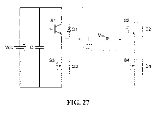
FIG, 27 shows a mono-phase dual switching frequency hybrid power converter
according to another embodiment of the invention.
FIG. 28 illustrates the voltage and the current across the load shown in FIG.
27.
FIG. 29A and 29B show a portion of a sequence; for controlling the switching
elements of the converter of FIG. 27, according to one embodiment.
FIG. 30 illustrates the current across an inductive load, according to one
embodiment.
FIG. 31A and 318 show a portion of a sequence for controlling the switching
elements of the converter of FIG. 27, according to ar ather embodiment.
FIG. 32 shows control signals operating switching elements S9 to S4 of FIG.
27,
according to one embodiment.
FIG. 33 illustrated a three-phase power converter, according to one
embodiment.
FIG. 34A and 34B are tables showing the overall, losses for a typical power
converter and a dual switching frequency hybrid power converter, according to
one embodiment.
FIG. 35 is a flow chart illustrating an embodiment of a method for voltage
conversion between a first element and a second element.
Further details of the invention and its advantages; will be apparent from the
detailed description included below.
DETAILED DESCRIPTION
In the following description of the embodiments, references to the
accompanying
drawings are by way of illustration of an example by Which the invention may
be
-15-
CA 02763444 2011-11-24
WO 2010/145019 PCT/CA2010/000919
practiced. It will be understood that other embodiments may be made without
departing from the scope of the invention disclosed.
As previously described, the power converters of the prior art generally use a
single type of switching elements for effecting the power conversion.
Switching
elements presenting low conduction losses such aS the IGBTs however present
a low commutation speed and high commutation flosses. On the other hand,
switching elements presenting low commutation losses such as the MOSFETs
however present high conduction losses.
Moreover, as known to the skilled addressee, each Of the IGBT and the MOSFET
may be provided with an integrated anti-parallel diode. While the diode
integrated
to an IGBT generally presents a fast operating speed, the diode integrated to
a
MOSFET has a much more lower operating speed.
According to one embodiment, a hybrid converter is disclosed which uses two
different types of switching elements and wherein each type of switching
element
is used in an optimal configuration to reduce the overall output losses of the
converter.
Referring to FIG. 18, there is shown a mono-phase dual switching frequency
hybrid power converter according to an embodirhent of the invention. As
illustrated, the converter uses two different types of switching elements: a
first
switching element having low conduction losses such as an IGBT and a second
switching element having low commutation losses such as a MOSFET. The load
is a resistive load.
Throughout the present description, exemplary embodiments of the dual
switching frequency hybrid power converter will be described with IGBTs as the
first switching elements and MOSFETs as the second switching elements but the
skilled addressee will appreciate that other arrangements may be considered,
as
long as the first switching elements have suitable lowiconduction losses and
the
-Is-
CA 02763444 2011-11-24
WO 2010/145019 PCT/CA2010/000919
second switching elements have suitable low commutation losses. For non-
limitative examples, thyristors, OTC, IGCT, MCT or specific types of MOSFETS
presenting low conduction losses may be used fori the first switching
elements.
Moreover, specific fast IGBTs may be used for the second switching elements.
As it will be more clearly detailed below, the MOSFETs, i.e_ the second
switching
elements, are switched at a high frequency since they are fast and present low
commutation losses while the IGBTs are switched at a low frequency since they
are much slower. Moreover, in order to reduce even more the overall losses of
the converter, the IGBTs, which have low conduction losses, are used more
often
than the MOSFETs, i.e. they are more often in a conduction state than the
MOSFETs, as shown in FIG. 19 and detailed below-
Moreover, in one embodiment, for example in the case the load is a resistive
load
only, the anti-parallel diodes that are generally integrated to the MOSFETs
are
not used, which is of great advantage since they are slow and dissipative when
switched at a high frequency. As it will be more clearly understood upon
reading
of the present description, the described topolbgy becomes even more
advantageous when a plurality of MOSFETs is connected in a parallel
relationship to provide more current power.
The skilled addressee will appreciate that this particular arrangement enables
to
greatly reduce the output losses of the converter while providing a high
switching
frequency. This high switching frequency enables to reduce the size of the
passive components (the capacity and the inductor in the embodiment
illustrated
in FIG. 4) and the overall cost of the converter, wl ich is of great
advantage,
particularly in the case where the power converter is provided on a printed
circuit
2.5 board.
The dual switching frequency hybrid power converter, will now be described
with
reference to FIG. 18 which shows a mono-phase; converter but the skilled
-17-
CA 02763444 2011-11-24
WO 2010/145019 PCT/CA2010/000919
addressee will appreciate that three phase and multi-phase power converters
may be provided according to the principles described herein, as further
described thereinafter with reference to FIG. 20.
Referring to FIG. 18, there is shown a dual switchhing frequency hybrid power
converter adapted to be connected between a first element and a second
element for voltage conversion, i.e. a DC elemenfi and an AC element in the
illustrated case. In the illustrated case, the converter is used for
converting a DC
voltage to an AC voltage but it should be understood that conversion from an
AC
source to a DC source may also be performed, as well as a DG to DC conversion
or even an AC to AC conversion, as detailed thereinafter.
The dual switching frequency hybrid power converter comprises a first leg
electrically connected to the DC element, a DC power source in the illustrated
case. The first leg comprises a high side switch add a low side switch
serially
connected. The high side switch comprises a selected one of a first switching
element having low conduction losses and a secon i switching element having
low commutation losses. In the illustrated embodiment, the high side switch of
the first leg comprises an IGBT.
The low side switch comprises the remaining of a first switching element
having
low conduction losses and a second switching element having low commutation
tosses. In the illustrated case, the low side switch of the first leg
comprises a
MOSFET since an IGBT has been selected for the sigh side switch of the first
leg. The skilled addressee will nevertheless appreciate that an inverted
configuration may be selected.
The first leg further comprises an anti-parallel diode operatively connected
in a
parallel relationship with the IGBT. In one embodimjsnt, the anti-parallel
diode
may be integrated to the !GBT but the skilled addressee will appreciate that a
diode not integrated with the IGBT may be a(ternativelg used.
-18-
CA 02763444 2011-11-24
WO 2010/145019 PCT/CA2010/000919
The dual switching frequency hybrid power conveirter comprises a second leg
electrically connected to the DC source in a parallel; relationship with the
first leg,
The second leg comprises a high side switch and a low side switch serially
connected. The high side switch comprises a selebted one of a first switching
element having low conduction losses and a second switching element having
low commutation losses corresponding to the one selected for the high side
switch of the first leg. In other words, the selection of the type of
switching
elements that is made for the second leg depends on the selection used for the
first leg_ In the illustrated case, the high side switch of the second leg
comprises
an (OBT since the high side switch of the first leg comprises an 1GBT.
The low side switch of the second leg comprises the remaining of a first
switching
element having low conduction losses and a second switching element having
low commutation losses. In the illustrated case, the law side switch of the
second
leg comprises a MOSFET since an IGBT has been selected for the high side
switch of the second leg.
The second leg further comprises an anti-parallel diode operatively connected
in
a parallel relationship with the IGBT. In one embodiment, the anti-parallel
diode
may be integrated to the IGBT but the skilled addressee will appreciate that a
diode not integrated with the IGBT may be used.
As it will be more clearly detailed below, each of the first switching
elements is
operated at a tow fundamental frequency and each of the second switching
elements is operated at a high frequency greater than the low fundamental
frequency.
In one embodiment, the low fundamental frequency is comprised between 1 Hz
and 1000 Hz. In a further embodiment, the low fundamental frequency is 60 Hz
while in another embodiment, the low fundamental frequency is 50 Hz_
-19-
CA 02763444 2011-11-24
WO 2010/145019 PCT/CA2010/000919
In one embodiment, the high frequency is comprised between 1 kHz and I MHz
although greater values may also be considered fora given application.
The skilled addressee will appreciate that various arrangements may be
envisaged for the low fundamental frequency and tho high frequency, as tong as
the two frequencies are distinct enough.
FIG. 19 illustrates the general principle of the (switching of the switching
elements.
Referring to FIGs. 21 to 23, an exemplary embodiment of the control signals
used to operate the switching elements S1 to S4 of Fig- 18 will be described.
The
skilled addressee will appreciate that each of these control signals is
electrically
connected to the gate of the corresponding switching element to command a
conducting state or a blocked state thereof.
In the illustrated embodiment, as shown in FIG. 21, a sinusoidal reference is
compared with a triangular carrier signal to produce the low-side control
signals.
When the sinusoidal reference is greater than the carrier signal, the control
signal
for the switching element 54 is high and when the sinusoidal reference is
lower
than the carrier signal, the control signal for the switching element S4 is
low, The
control signal for the switching element S1 is high when the sinusoidal
reference
is positive while it is low when the sinusoidal reference is negative. In
other
words, the switching element S 1 is operated at the same low frequency than
the
sinusoidal reference while the switching element S , is operated at a greater
frequency.
FIG. 22 shows the generation of the control signal forithe switching elements
82
and 63. As illustrated, the sinusoidal reference used in FIG. 21 is inverted
and
compared to the same triangular carrier signal. When the sinusoidal reference
is
greater than the carrier signal, the control signal for tI7e switching element
S3 is
high and when the sinusoidal reference is lower than the carrier signal, the
-20-
CA 02763444 2011-11-24
WO 2010/145019 PCT/CA2010/000919
control signal for the switching element S3 is IoW. The control signal for the
switching element S2 is high when the sinusoidal reference is positive while
it is
low when the sinusoidal reference is negative. la other words, the switching
element 52 is operated at the same low frequency than the sinusoidal reference
while the switching element S3 is operated at a greater frequency.
As better shown in FIG. 23, a single one of the high side switching elements
S1
and S2 is activated at the same time. Moreover, ~ single one of the low side
switching elements S3 and 84 is activated at the same time. Furthermore, a
single one of the switching elements of the same leg is also activated at the
same time.
In section A of FIG. 23, it can be seen that the control signal for the
switching
element S1 is high while the control signal for the switching element S4 is
alternatively switched between a low state and a high state. The control
signals
for S2 and S3 are low so that 62 and 83 do not conduct. When both control
signals for S1 and S4 are high, the load is connected to the DC voltage, as
shown in FIG. 24A, so that the current therein is increasing.
When S4 is turned OFF, the current of the load runs through D2 and S1, as
shown in FIG. 24B, so that the current slightly decreases. This sequence is
operated as long as S1 is in its high state.
In section E3 of FIG. 23, it can be seen that the control signal for the
switching
element 82 is high while the control signal for the switching element S3 Is
alternatively switched between a low state and a high state. The control
signals
for S1 and S4 are low so that S1 and 84 do not conduct. When both control
signals for S2 and 83 are high, the load is connected to the DC voltage, as
shown in FIG. 24C, so that the current therein is increasing-
-21-
CA 02763444 2011-11-24
WO 2010/145019 PCT/CA2010/000919
When 83 is turned OFF, the current of the load runs through D1 and S2, as
shown in FIG. 24D, so that the current slightly dlecreases. This sequence is
operated as long as S2 is in its high state.
Then, Si and S4 are used again, as in section A.
The skilled addressee will appreciate that this embodiment of an operating
sequence enables to not use the diode of the MOSFETs, which if of great
advantage, as previously explained.
The skilled addressee will appreciate that the above described operating
sequence of the switching elements is suitable for the cases wherein the load
is
a resistive load. However, the skilled addressee viiiil also appreciate that
the
described sequence may not be suitable for a capacitive or an inductive load,
i.e.
the power factor of the brad is lower than 1.
Indeed, referring to FIG. 27, according to the principio of the invention,
when the
voltage and the current across the load are both positive, S1, S4 and D2 are
activated, S4 enables the modulation. When S4 is stopped, D2 becomes active
and enables a free wheel operation therethrough. When the voltage and the
current across the load are both positive, S2, S3 : and D1 are activated. 83
enables the modulation. When S3 is stopped, D1 becomes active and enables a
free wheel operation therethrough.
As shown in FIG. 28, in the case where the load is a capacitive load or an
inductive load, there is a phase difference between the voltage and the
current
across the load. The operating sequence of the power converter should be
adapted to this particular case.
Indeed, when the voltage becomes negative but the current is still positive,
S1
and 84 stop. Because of the voltage across the load, D2 and D3 conduct, as
-22-
CA 02763444 2011-11-24
WO 2010/145019 PCT/CA2010/000919
illustrated in FIG. 29A. Since D2 and D3 conduct, S2 and 83 cannot be
activated
and the operating sequence for converting the voltage cannot be performed.
Similarly, when the voltage becomes positive but the current is still
negative, D1
and D4 conduct and prevent the activation of $1 and S4, as illustrated in FIG.
29B. In this case, one can not modulate the voltage of the load in order to
provide a sinusoidai current. Indeed, as illustrated in FIG. 30, this
phenomena
will create a distortion of the current, which lis unacceptable for given
applications.
Referring now to FIG. 31A and 31 B, in order to overcome this issue, D1 and D2
may be blocked to prevent their conduction according to a given sequence. This
enables a sinusoidal modulation of the current, which' is of great advantage.
For example, in one embodiment, when the voltage becomes negative but the
current is still positive, S4 is triggered in order to blodk D2. If D2 and D3
conduct,
the current decreases linearly in a fast manner- On the contrary, when 84 is
triggered, D2 becomes blocked and the current across the load still decreases,
but more slowly. Thus, it becomes possible to modulate the current across the
load with the control signals controlling S4. In this manner, a sinusoidal
current
may be obtained.
In this embodiment, the control signal controlling Sy is similar to the
inverted
control signal controlling S3, as previously detailed for the case of a
resistive
load. FIG. 32 illustrates the control signal for Si to~ 84 for the case of a
load
which is not a resistive one.
White the operating sequence of the switching elements has been described for
a mono-phase converter, the skilled addressee willi appreciate that it can be
adapted for a three-phase or any multi-phase converter. Moreover, the skilled
addressee will also appreciate that a voltage conversion from an AC source to
a
DC source may also be implemented.
-23-
CA 02763444 2011-11-24
WO 2010/145019 PCT/CA2010/000919
In one embodiment, the dual switching frequency hybrid power converter further
comprises a third leg electrically connected to the first element in a
parallel
relationship with the first leg and the second leg. The third leg comprises a
high
side switch and a low side switch serially connected, the high side switch
comprising a selected one of a first switching elerihent having low conduction
losses and a second switching element having low commutation losses
corresponding to the one selected for the high side switch of the first leg,
as
previously detailed. The low side switch comprises the remaining of a first
switching element having low conduction losses and ja second switching element
having low commutation losses. The third leg further comprises an anti-
parallel
diode operatively connected in a parallel relationship with the first
switching
element, thereby providing a three phase power converter.
FIG. 20 illustrates a three-phase converter comprising a third leg wherein a
plurality of elementary switching elements of the; same type is connected
together in a parallel relationship in order to enable more current in each of
the
semi-legs of the converter. This arrangement is of great advantage for
reducing
output losses of the converter since the diode of the MGSFETs are still not
used.
The above-described topology has been tested and validated with simulation
tools, as better shown in FIGs. 25 and 26. FIG. 25 illustrates the overall
losses
for different configurations of a three-phase converter for a switching
frequency
of 20 kHz while FIG. 26 illustrates the overall losses for different
configurations of
a three-phase converter for a switching frequency of 200 kHz. FIG. 25 shows
that
the overall losses of a converter may be reduced by a factor 4 when using a
configuration similar to the one described above at a~ switching frequency of
20
kHz_ FIG. 26 shows that the overall losses of a converter may be even more
reduced when using a configuration similar to the one described above at a
switching frequency of 200 kHz.
-24-
CA 02763444 2011-11-24
WO 2010/145019 PCT/CA2010/000919
Referring now to FIG. 33, there is shown another embodiment of a three-phase
dual switching frequency hybrid power converter fbr a three-phase load. The
three-phase power converter comprises a first, a second and a third dual
switching frequency hybrid power converter as previously defined. Each of the
first, second and third power converter is operatively connected to a
corresponding phase of the three-phase load. Although three DC power sources
are shown, it should be mentioned that a single DC power source may be used.
The neutral conductor of the load is operatively connected to each of the
three
power converter, as illustrated.
The embodiment shown in FIG. 33 is of great advantage with respect to the
typical power converters of the art. Indeed, with this embodiment, the
required
DC voltage may be lower than in the case of a typical power converter in order
to
generate a given output voltage. For example, a DC ivoltage of 490V is
required
to generate an output voltage of 347V between one of the phases and the
neutral
conductor. With a three-phase power converter of the prior art having three
legs,
a DC voltage of 848V is required in order to provide the same output voltage
of
347V.
The above disclosed embodiment is of great advantage since it enables to
greatly reduce the overall losses of the power converter. Indeed, the required
switching elements may have a reduced size singe they are adapted for a
reduced voltage. These switching elements may thus be faster, thereby reducing
the losses associated to the commutation time. Moreover, since the DC voltage
is reduced, the commutation losses may also be reduced.
FIG. 34A and 34B show the overall losses simulated for a power converter
according to the invention and a typical power converter respectively. The
simulation has been made for an output power of 200 kW with a power factor of
0.8, a voltage of 347 V between a phase and the neutral conductor and a
current
of 240 Arms with a DC power source of 570 V.
-25-
CA 02763444 2011-11-24
WO 2010/145019 PCT/CA2010/000919
With a typical power converter, there are three IGBTs mounted in parallel for
each switching element, for a total of 18 IGBTs. The; used switching frequency
is
20 kHz_ FIG. 34A shows the losses. The switching elements have a reduced
speed since they are adapted for a high voltage, i.e. the DC bus is at 1000 V.
This increases the losses.
FIG. 34A shows the losses with a three phase power converter comprising three
mono-phase power converter according to the invention. The high-side switches
are operated at a low fundamental frequency of 60 Hz. Each mono-phase power
converter comprises 12 IGBTs, thus the three-phase power converter comprises
361GBTs.
The switching elements have been chosen to support two times the voltage of
the DC source. One can see that the commutation ; losses are greatly lowered
with respect to the typical power converter, which is of great advantage.
The conduction losses are however greater since more switching elements
conduct at the same time. The skilled addressee will nevertheless appreciate
that
the overall losses are reduced by a factor of 3.5 with respect to a typical
power
converter.
The skilled addressee will appreciate that the dual 'switching frequency
hybrid
power converter as previously defined may be used for converting an AC voltage
into a DC voltage or for converting a DC voltage into; an AC voltage or even
for
converting an AC voltage into another AC voltage. As previously mentioned, a
conversion from a DC voltage to another DC voltage may also be considered.
The conversion is done between a first element and a second element. The first
element and the second element being a DC voltage source and a DC load.
According to another aspect, there is also providbd a method for voltage
conversion between a first element and a second element, as illustrated in
FIG.
35.
-26-
CA 02763444 2011-11-24
WO 2010/145019 PCT/CA2010/000919
At processing step 3510, a dual switching frequency hybrid power converter as
previously defined is provided.
At processing step 3520, the dual switching frequenccy hybrid power converter
is
operatively connected between the first element and the second element.
At processing step 3530, a plurality of control sign;ls is generated, each
being
adapted for controlling a corresponding one of the stitching elements.
At processing step 3540, the control signals are applied to the corresponding
switching elements to thereby enable the voltage conversion between the first
element and the second element.
Although the above description relates to specific preferred embodiments as
presently contemplated by the inventors, it will be understood that the
invention
in its broad aspect includes functional equivalents of the elements described
herein. For example, throughout the present description and in the
illustrating
Figures, the selected high side switching elements comprise IGBTs and the
selected low side switching elements comprise MOSFETs. The skilled addressee
will appreciate that the IGBTs may be used for the tow side switching elements
while the MOSFETS may be used for the high side switching elements, as long
as the operating sequence thereof is adapted to use each type of switching
elements in its optimal frequency range, as detailed above.
-27-