Note: Descriptions are shown in the official language in which they were submitted.
CA 02764684 2014-05-14
1
CIRCUIT ARRANGEMENT AND METHOD FOR INDUCTIVE ENERGY
TRANSFER
FIELD OF THE PRESENT DISCLOSURE
The present disclosure relates to a circuit arrangement for inductive energy
transfer for
small electrical devices, for example for an electric toothbrush or for an
electric shaving
apparatus.
Background of the Present Disclosure
Battery-operated small electrical devices are typically charged at an external
charging
station. Contactless charging stations that inductively transmit electric
energy from the
charging station to the device are especially preferred. For this, an
alternating magnetic
field is generated in the charging station by an oscillator that includes a
coil element and
a capacitor element, wherein the coil element simultaneously forms the primary
coil of an
inductive transformer and the secondary coil of the transformer is arranged in
the device
to be charged. The charging station is therefore conventionally designated as
the primary
side and the device to be charged is designated as the secondary side. Such a
charging
station in which the oscillator is operated with a stabilized voltage or,
respectively,
oscillates with a uniform amplitude is known from JP 06-054454 A.
Modern charging stations typically have three operating states. The first
state is the
operating mode in which the secondary side continuously draws power, for
example to
operate the device or to charge a cell installed in the device. The second
state is the
simple standby mode in which the device is not located in the charging
station, thus in
which no power whatsoever is drawn. The third state is what is known as the
extended
standby mode in which the device is located in the charging station but only
requires
CA 02764684 2014-05-14
2
power intermittently, for example because -- although the cell is fully
charged -- it must
occasionally be recharged to compensate for the self-discharge or for the
device's own
power consumption. In the latter cited case, the charging station should
switch back and
forth between the simple standby mode and the operating mode as needed. The
respective
operating state of the charging station (primary side) is thus determined by
the power
demand of the small electrical device (secondary side).
It is known to detect the power demand of the secondary side directly at the
secondary
side, to transfer corresponding information to the primary side and to adjust
the oscillator
- meaning, for example, the base emitter voltage of a transistor operating in
the oscillator
- accordingly. This solution is quite complicated because transmission means
for the
information from the secondary to the primary side are required.
Alternatively, the power
demand of the secondary could be determined by measuring the power consumption
of
the oscillator (at the primary side) and controlling the oscillator
accordingly. However,
both variants are poorly suited to the setting of multiple operating states
because the
power consumption of the charging station is only slightly affected by the
power
consumption of the device due to the typically weak coupling between the
primary and
secondary side of the transformer.
An aspect of the present disclosure is to specify a circuit arrangement for
inductive power
transfer from a primary side to a secondary side that may establish the power
demand of
the secondary side at the primary side in a simple manner.
Solution According to the Present Disclosure
Disclosed is a circuit arrangement for the inductive transmission of energy,
which circuit
arrangement has an oscillator and a device to detect the load of the
CA 02764684 2011-12-07
3
oscillator and to switch the circuit arrangement into one of multiple
operating states (for
example a standby mode or an operating mode) depending on the detected load,
wherein
the device is designed to evaluate an electrical variable in the oscillator.
The oscillator is
preferably a Colpitts oscillator or a Hartley oscillator and has an active
element known
per se. The device for detecting the load of the oscillator evaluates an
electrical variable
in the oscillator, preferably a voltage at a terminal of the active element.
The active
element is, for example, a transistor that is preferably operated in a common
base. The
device for detecting the load of the oscillator preferably evaluates a voltage
at a collector
or at the base of the transistor, for example a semioscillation with a
predetermined
polarity. Preferably, the amplitude or the mean value of the negative voltage
at the
collector or at the base of the transistor is evaluated. Namely, the amplitude
of the half-
wave of the oscillator oscillation varies particularly strongly depending on
the secondary
side load. The load of the oscillator - and therefore the power demand of the
secondary
side - may thus be determined at the primary side using an electrical variable
that is
detectable in the oscillator. The device compares the detected load with a
reference value
and, depending on the result of the comparison, adjusts the operating state of
the circuit
arrangement, for example by activating a controllable switch with which the
circuit
arrangement may be switched from a standby mode into an operating mode or vice
versa.
The switching from standby mode into the operating mode and vice versa may,
for
example, take place by switching the supply voltage of the oscillator via a
controllable
switch. For example, if the circuit arrangement has a power adaptor with a
complex input
resistance (preferably, a capacitive series resistor), the active power
consumption of the
circuit arrangement may, for example, be varied by terminating the output of
the power
adaptor with a comparably small resistance by means of the controllable switch
(standby
mode). The mains then experiences an essentially capacitive reactive load that
is defined
by the capacitive series resistor. However, the capacitive series resistor of
the power
adaptor may also be variable via the controllable switch, for example by
switching the
capacitance of the capacitive series resistor. However, the oscillator may
also have a
CA 02764684 2011-12-07
4
damping element that is variable via the controllable switch, meaning that the
power
consumption of the oscillator may be switched. In standby mode the oscillator
may either
be so significantly attenuated by the damping element, that said oscillator
oscillates but
only with a small amplitude, or it may be so strongly equalized that the
oscillator
represents a comparably small load resistance for the power adaptor, and the
power
consumption from the mains is determined by the capacitive series resistor of
the power
adaptor, thus essentially comprising a reactive power.
In order to satisfy the EU 205/32 Guideline it is sufficient if the power
consumption of
the circuit arrangement in standby mode is lower than the power consumption in
the
operating mode only as an average over time. Accordingly, the oscillator in
standby mode
may, for example, operate intermittently, meaning that it oscillates
intermittently with
lower amplitude and otherwise oscillates with the larger amplitude typical in
operating
mode.
The described circuit arrangements are particularly suitable for use in
inductive charging
stations for small electrical devices, for example for electric toothbrushes,
electric
shaving apparatuses or communication devices (mobile telephones).
Brief Description of Figures
The present disclosure is explained using exemplary embodiments that are
presented in
the drawings. Additional variants of the circuit arrangements are mentioned in
the
description.
FIG. I a block diagram of a circuit arrangement for inductive energy transfer;
FIG. 2 a first circuit arrangement with a Hartley oscillator;
FIG. 3 a second circuit arrangement with a Hartley oscillator;
FIG. 4 a first circuit arrangement with a Colpitts oscillator;
FIG. 5 a second circuit arrangement with Colpitts oscillator;
CA 02764684 2011-12-07
FIG. 6 a third circuit arrangement with a Colpitts oscillator.
DETAILED DESCRIPTION OF FIGURES
The block diagram according to FIG. 1 shows a circuit arrangement with a power
adaptor
5 N and a self-oscillating oscillator LC that serves to generate an
alternating magnetic field.
The oscillator has a coil that serves to transmit inductively electrical
energy from the
oscillator LC (primary side) to a load (secondary side) not shown in the
Figure, for
example a small electrical device that for this purpose contains a receiver
coil that may be
coupled to the coil of the oscillator. The oscillator draws electrical energy
from the mains
V3 via the power adaptor N, which has a complex input resistance. The circuit
arrangement also has a controllable switch T2 and a device X1 for detecting
the load of
the oscillator LC, which device XI controls the switch T2. The complex input
resistance
of the power adaptor N may be switched via the controllable switch T2 so that
the circuit
arrangement consumes a lower active power from the mains V3 in a standby mode
than
in an operating mode. The controllable switch T2 may be realized, for example,
by a relay
or a transistor that may be activated electrically or optically.
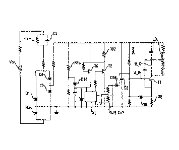
In the circuit arrangement shown in FIG. 2, the power adaptor includes a
capacitor Cl as
a capacitive series resistor and a rectifier bridge with diodes Dl, D2, D3, D4
which,
together with a capacitor C2, generates from the alternating mains voltage a
smoothed
direct voltage with which the oscillator LC is operated. A resistor R2 is
connected in
parallel with the capacitor Cl, which resistor R2 ensures that the capacitor
Cl is
discharged after the power adaptor has been disconnected from the mains V3.
The resistor
R2 is relatively high-resistance in comparison to the active resistance of the
capacitor Cl,
such that the complex input resistance of the power adaptor is essentially
defined by the
capacitive resistance of the capacitor Cl.
If the circuit arrangement should be placed in standby mode, the capacitive
series resistor
is connected to ground via the rectifier bridge and a transistor T2 and a
resistor R22. The
CA 02764684 2011-12-07
6
power consumption of the circuit arrangement from the mains is thereby shifted
from the
active power range in the direction of the reactive power range, and a
reduction of the
active power consumption from the mains is thus achieved. If the transistor T2
is
completely conductive, the current is essentially limited by the resistor R22
and the
capacitor Cl. If the resistance value of R22 is zero, the oscillator is
completely
disconnected from the energy supply. The mains then experiences a purely
capacitive
reactive load. However, the resistor R22 is preferably dimensioned so that,
given a
conductive transistor T2, a voltage is set at the capacitor C2 that is still
sufficient for
operation of the oscillator, wherein this then still oscillates but with a
reduced amplitude.
The oscillator LC included the circuit arrangement is a Hartley oscillator in
a common
base that has a transistor Ti as an active element. For detection of the load
of the
oscillator by the secondary side, a device X1 (a microcontroller, for example)
is provided,
as well as a diode D15 and a voltage divider that is formed by the resistors
R16 and R17.
The negative half-wave of the base voltage U_B of the transistors Ti is
applied at one end
of the voltage divider R16, R17. This voltage U_B is fed via the diode D15 and
represents the load of the oscillator LC. A positive reference voltage that is
generated by
the microcontroller X1 is applied at the other end of the voltage divider R16,
R17. The
voltage at the center tap of the voltage divider R16, R17 is supplied to the
microcontroller
Xl. The negative base voltage U_B of the transistor Ti is transformed by means
of the
voltage divider R16, R17 into the positive voltage range so that it may be
compared with
a reference value by the microcontroller XI. The microcontroller X1 activates
the
transistor T2 depending on the result of this comparison. Instead of the
negative half-
wave of the base voltage, the negative half-wave of the collector voltage U_C
may also
be evaluated.
The microcontroller X1 is also supplied with energy from the power adaptor via
a voltage
divider with a resistor R15, a diode D14 and a transistor T5 when the
transistor T2 is
conductive and the circuit arrangement is in standby mode. As soon as it
establishes an
CA 02764684 2011-12-07
7
increased power demand of the secondary side, it will disable the transistor
12 again. The
microcontroller X1 may be provided with a control program which, for example,
switches
the transistor T2 on and off according to a predetermined time schedule.
Instead of the Hartley oscillator, another embodiment of the circuit
arrangement described
above uses a Colpitts oscillator and/or uses discrete circuits - instead of a
microcontroller
- to detect the load of the oscillator and to modify the complex input
resistance of the
power adaptor, for example as they are shown in FIG. 4 through 6.
FIG. 3 shows a circuit arrangement with a Hartley oscillator that is supplied
by a power
adaptor with a capacitive series resistor Cl. What is known as a reset IC is
present as a
device X1 to detect the load of the oscillator. The reset IC only outputs a
high level at its
output Vout when its supply voltage exceeds a predetermined value. A switching
threshold for a field effect transistor 13 to become conductive is set with
the reset IC. The
energy supply from the power adaptor into the oscillator is set by evaluating
the base
voltage of the transistor Tl. For this, the negative base voltage of the
transistor Ti is
supplied to the reset IC via the diode D15. The base of the transistor Ti is
coupled with
the oscillating circuit via the emitter resistor R5 and the diode D5.
If the inductive load of the oscillator increases, the voltage at the base of
the transistor Ti
decreases. The diode D15 only allows a current flow when the voltage U15 is
negative,
thus when the base voltage at the transistor Ti is negative to ground. The
reset IC draws
its supply voltage via the diode D15. Capacitors C15 and C16 that are arranged
between
ground and the anode of the diode DI5 set a time constant, with which changes
of the
base voltage affect the reset IC. The reset IC only outputs a high level at
its output Vout
when the negative half-wave of the base voltage of the transistor Ti falls
below a
predetermined value. The field effect transistor T3 (which for its part
switches the
transistor T2 to the conductive state) is activated with the level Vout. If
the negative base
voltage of T1 falls below a predetermined value, the output of the power
adaptor is
shorted with a comparably small resistance via the ohmic resistor R22. Due to
the
CA 02764684 2011-12-07
8
capacitive series resistor Cl, the power adaptor now consumes almost
exclusively a
reactive power from the mains, and the oscillator LC receives only little
electric energy
from the power adaptor until the voltage at the capacitors C15 and C16 has
declined to
the point that the supply voltage of the reset IC has again fallen below a
predetermined
value. In standby operation, therefore, the oscillator alternately oscillates
with a small
amplitude or, respectively, a large amplitude.
FIG. 4 shows a circuit arrangement with a Colpitts oscillator that is supplied
by a power
adaptor with a capacitive series resistor Cl. The device X1 for detecting the
load of the
oscillator includes a Zener diode D10 and a diode D 11 that detects the
negative voltage
amplitude of the oscillation in the oscillator LC, namely at the collector of
the transistor
TI. In the unloaded state of the oscillator, the negative voltage amplitude is
maximum in
terms of magnitude (reference value). If the amplitude is less than the
reference value,
this is an indication of a stronger attenuation, thus of a higher power
demand. In the case
of the unloaded oscillator, the branch with the Zener diode D10 and the diode
Dll is
conductive, such that the transistor T4 is conductive. The transistors T3 and
T5 may
likewise be conductive when their base emitter voltages exceed a predetermined
value in
terms of magnitude. The two transistors T3 and T5 control the field effect
transistor T2. If
12 is conductive, the output of the power adaptor is connected to ground via
the ohmic
resistor R22 (which has a predetermined, relatively small value), such that
the supply
voltage of the oscillator LC decreases and draws barely any more energy from
the power
adaptor. Due to the capacitive series resistor CI (which has a high value in
comparison to
the ohmic resistor R22), the mains is loaded practically only with a reactive
power
(standby operation).
The diode D9 at the collector of the transistor T1 suppresses a possible
return current
flow in the reverse direction of the transistor T1, which would be borne by
the diode
branch Dl 0, D11, thus supporting the ability to evaluate the negative voltage
amplitude in
the oscillator LC.
CA 02764684 2011-12-07
9
In the circuit arrangement shown in FIG. 5, the power adaptor comprises a
complex input
resistance whose capacitive portion may be varied depending on the load of the
oscillator.
The power adaptor includes a capacitive series resistor and a rectifier bridge
with diodes
D1, D2, D3, D4 that, together with a capacitor C2, generate from the
alternating mains
voltage a smoothed direct voltage with which the oscillator is operated. The
capacitive
series resistor has a capacitor C7 and a capacitor Cl with which a resistor R2
is wired in
parallel. The resistor R2 ensures that the capacitor Cl is discharged after
the power
adaptor N has been disconnected from the mains V3. An electronic switch is
wired in
parallel with the capacitor C7, which electronic switch includes two
transistors connected
to in series M3, M4 and is part of an optocoupler. The parallel wiring made
up of capacitor
Cl and resistor R2 is wired in series with the parallel wiring made up of
capacitor C7 and
the transistors M3, M4. The resistor R2 is relatively high-resistance in
comparison to the
active resistance of the capacitor Cl. The complex input resistance of the
power adaptor
N is essentially defined by the capacitive resistance of the capacitor Cl when
the
electronic switch is closed or, respectively, by the capacitive resistance of
the two
capacitors Cl and C7 wired in series when the electronic switch is open.
If the circuit arrangement should be set into standby mode, the electronic
switch is
opened, meaning that the diode Dl 2 of the optocoupler is deactivated. The
active power
consumption of the circuit arrangement from the mains is thereby reduced
because the
active resistance of the two capacitors Cl, C7 wired in series is
significantly greater than
the active resistance of the capacitor Cl. The power adaptor now consumes
nearly only
reactive power. Preferably, the capacitors Cl, C7 are dimensioned so that in
standby
mode a voltage that is still sufficient to operate the oscillator arises at
the capacitor C2,
wherein this oscillator oscillates with only a reduced amplitude.
The oscillator included in the circuit arrangement is a Colpitts oscillator in
a common
base, which Colpitts oscillator has a transistor TI as an active element. To
detect the
loading of the oscillator by the secondary side, a circuit is provided that
has two diodes
CA 02764684 2011-12-07
D 1 0, D13, two resistors R13, R14, a capacitor CO and a switching transistor
M6. The
cathode of the diode D10 is connected with the collector of the transistor Ti.
The
negative half-wave of the collector voltage U_C of the transistor T1 occurs at
the anode
of the diode D10. This voltage is representative of the load of the oscillator
LC. Instead of
5 the negative half-wave of the collector voltage, the negative half-wave
of the base voltage
U_B may also be evaluated. The anode of the diode D10 is connected via the
resistor R13
with the one end of the capacitor C6 and the cathode of the diode D13. The
other end of
the capacitor CO is connected to ground. The anode of the diode D13 is
connected with
the control terminal of the switching transistor M6 and to ground via the
resistor R14.
10 The contact gap of the switching transistor M6 is wired in series with
the diode D12 of
the optocoupler and at least one current limiting resistor R18.
The switching transistor M6 is only disabled when a sufficiently high negative
voltage is
applied at its control terminal. Given a low load of the oscillator, a
sufficiently high
negative voltage is supplied to the control terminal of the switching
transistor M6 via the
diodes D10 and D13 and the resistor R13, which has the result that the diode
D12 of the
optocoupler is deactivated, the transistors M3, M4 of the electronic switch
are disabled
and the complex input resistance assumes a high value.
Instead of the optocoupler and capacitor C7, another embodiment of the circuit
arrangement described above uses a series circuit made up of a transistor T2
and a resistor
R22 parallel to the capacitor C2 (as is shown in FIG. 2) or a switchable
emitter resistor in
the oscillator (as is shown in FIG. 6) to vary the complex input resistance of
the power
adaptor.
FIG. 6 shows a further circuit arrangement with a Colpitts oscillator in a
common base,
which circuit arrangement is designed to detect the negative voltage amplitude
of the
oscillation in the oscillator LC. If the negative voltage amplitude exceeds a
predetermined
value in terms of magnitude -- thus in the case of the unloaded oscillator LC -
- a branch
CA 02764684 2011-12-07
11
with a Zener diode 1)10 and a diode DI I becomes conductive and a transistor
T3 is
conductive. The transistors 14 and T5 may likewise be conductive when their
base
emitter voltages exceed a predetermined value in terms of magnitude. The two
transistors
T4 and 15 control a field effect transistor 12 whose contact gap is wired in
parallel with
an emitter resistor R5. If 12 is conductive, the active resistance Z at the
emitter of the
transistor T1 is relatively low, such that the energy supply in the oscillator
LC is
maximum. However, the capacitive series resistor Cl of the power adaptor is
not
designed for such a high power, such that the output voltage of the power
adaptor -- and
therefore the active power consumption of the circuit arrangement -- is
reduced because
the output of the power adaptor is now terminated with a comparably low
resistance.
If the negative voltage amplitude decreases in terms of magnitude in
comparison to a
reference value that is determined by the Zener diode D10, this is an
indication of a
stronger attenuation, thus of a higher power demand at the secondary side. The
transistor
T2 is disabled and the active resistance Z at the emitter is comparatively
high. This is the
operating state of the circuit arrangement in which the power consumption of
the
oscillator is matched to the capacitive series resistor Cl of the power
adaptor and
maximum power is transmitted to the secondary.
A diode D9 at the collector of the transistors Ti suppresses a possible return
current flow
in the reverse direction of the transistor Ti which would be borne by the
diode branch
D10, D11, thus supports the ability to evaluate the negative voltage amplitude
in the
oscillator LC.