Note: Descriptions are shown in the official language in which they were submitted.
CA 02766062 2011-12-19
WO 2010/148402 PCT/US2010/039368
REFERENCE SIGNAL DESIGN FOR WIRELESS COMMUNICATION SYSTEM
BACKGROUND
[0001] The present invention relates generally to data transmission in mobile
communication systems and more specifically to useful resource block reference
signal
patterns as well as systems and method for using the patterns.
[0002] As used herein, the terms "user agent" and "UA" can refer to wireless
devices
such as mobile telephones, personal digital assistants, handheld or laptop
computers,
and similar devices or other User Equipment ("UE") that have
telecommunications
capabilities. In some embodiments, a UA may refer to a mobile, wireless
device. The
term "UA" may also refer to devices that have similar capabilities but that
are not
generally transportable, such as desktop computers, set-top boxes, or network
nodes.
[0003] In traditional wireless telecommunications systems, transmission
equipment in
a base station transmits signals throughout a geographical region known as a
cell. As
technology has evolved, more advanced equipment has been introduced that can
provide
services that were not possible previously. This advanced equipment might
include, for
example, an evolved universal terrestrial radio access network (E-UTRAN) node
B (eNB)
rather than a base station or other systems and devices that are more highly
evolved
than the equivalent equipment in a traditional wireless telecommunications
system. Such
advanced or next generation equipment may be referred to herein as long-term
evolution
(LTE) equipment, and a packet-based network that uses such equipment can be
referred
to as an evolved packet system (EPS). Additional improvements to LTE
systems/equipment will eventually result in an LTE advanced (LTE-A) system. As
used
herein, the phrase "base station" or "access device" will refer to any
component, such as
a traditional base station or an LTE or LTE-A base station (including eNBs),
that can
provide a UA with access to other components in a telecommunications system.
[0004] In mobile communication systems such as the E-UTRAN, a base station
provides radio access to one or more UAs. The base station comprises a packet
scheduler for dynamically scheduling downlink traffic data packet
transmissions and
allocating uplink traffic data packet transmission resources among all the UAs
communicating with the base station. The functions of the scheduler include,
among
others, dividing the available air interface capacity between UAs, deciding
the transport
1
CA 02766062 2011-12-19
WO 2010/148402 PCT/US2010/039368
channel to be used for each UA's packet data transmissions, and monitoring
packet
allocation and system load. The scheduler dynamically allocates resources for
Physical
Downlink Shared CHannel (PDSCH) and Physical Uplink Shared CHannel (PUSCH)
data
transmissions, and sends scheduling information to the UAs through a
scheduling
channel.
[0005] In LTE systems, data is transmitted from an access device to UAs via
Resource Blocks (RBs). Referring to Fig. 1, an exemplary resource block 50 is
illustrated
that is comprised of 168 Resource Elements (REs) (see exemplary elements 52)
arranged in twelve frequency columns and fourteen time rows as known in the
art.
Accordingly, each element corresponds to a different time/frequency
combination. The
combination of elements in each time row are referred to as an Orthogonal
Frequency
Division Multiplexing (OFDM) symbol. In the illustrated example the first
three OFDM
symbols (in some cases it may be the first two, first four, etc.) are reserved
for PDCCH
and are shown in Fig. 2 as gray REs collectively identified by numeral 56.
Various types
of data can be communicated in each RE.
10006] LTE systems employ various types of reference signals to facilitate
communication between an access device and a UA. A reference signal can be
used for
several purposes including, determining which of several different
communication modes
should be used to communicate with UAs, channel estimation, coherent
demodulation,
channel quality measurement, signal strength measurement, etc. Reference
signals are
generated based on data known to both an access device and a UA, and may also
be
referred to as pilot, preamble, training signals, or sounding signals.
Exemplary reference
signals include a cell specific or common reference signal (CRS) that is sent
by a base
station to UAs within a cell and is used for channel estimating and channel
quality
measurement, a UA-specific or dedicated reference signal (DRS) that is sent by
a base
station to a specific UA within a cell that is used for demodulation of a
downlink, a
sounding reference signal (SRS) sent by a UA that is used by a base station
for channel
estimation and channel quality measurement and a demodulation reference signal
sent
by a UA that is used by a base station for demodulation of an uplink
transmission from
the UA.
2
CA 02766062 2011-12-19
WO 2010/148402 PCT/US2010/039368
[0007] In LTE systems, CRS and DRS are transmitted by access devices in RB
REs.
To this end, see Fig. 2 which shows exemplary CRS (three of which are labeled
52) in
vertical, horizontal, left down to right and left up to right hatching for
ports 1 through 3
respectively and exemplary DRS in dark REs, three of which are labeled 54. The
reference signals allow any UAs communicating with the access device to
determine
channel characteristics and to attempt to compensate for poor characteristics.
The CRS
reference signals are base station/cell specific and UA-independent (i.e., are
not
specifically encoded for particular UAs) and, in at least some cases, are
included in all
RBs. By comparing the received CRS to known reference signals (i.e., known
data), a
UA can determine channel characteristics (e.g., a communication quality index,
etc.).
The difference between the known data and the received signal may be
indicative of
signal attenuation, path-loss differences, etc.
[0008] UAs report channel characteristics back to the access device and the
access
device then modifies its output (i.e., subsequent REs) to compensate for the
channel
characteristics. To indicate how signal output is modified, the access device
transmits
UA specific DRS to each UA. Here again, DRS data is known at the UA and
therefore,
by analyzing received DRS, UA can determine how the access device output has
been
modified and hence obtain information required to demodulate data received in
subsequent REs. In Fig. 2, exemplary CRS reference signals are indicated by
hatching,
DRS signals are indicated by dark REs and non-reference signal elements during
which
traffic data is transmitted are blank (i.e., white).
[0009] Referring again to Fig. 2, to avoid collisions LTE system DRS 54 are
generally
allocated to OFDM symbols separate from those occupied by CRS. Furthermore,
DRS
54 are generally allocated away from PDCCH 56. In release 8 LTE devices
(hereinafter
"Rel-8 devices"), for example, DRS of antenna port 5 may be specified for
PDSCH
demodulation as shown in Fig. 2. In some cases, CRS 52 on antenna ports 0-3
are
distributed on all RBs in the system bandwidth, while DRS 54 on antenna port
5, for
example, may only be allocated in RBs assigned to a corresponding UA. When a
UA is
assigned two or more contiguous RBs, DRS 54 allocation may simply be repeated
from
one RB 50 to the next.
3
CA 02766062 2011-12-19
WO 2010/148402 PCT/US2010/039368
[0010] One contemplated LTE-A requirement is to reach a peak spectrum
efficiency of
30bps/Hz. To fulfill this requirement, the total RE overhead for DRS will
likely be limited.
As such, in one system implementation satisfying peak spectrum efficiency
requirements,
a maximum of 24 DRS REs may be allocated to up to 8 antenna ports. As a
result, the
average number of REs in one RB for each antenna port becomes relatively
small. For
instance, for 8 antenna ports, 3 REs per RB may be allocated for each of 8 DRS
antenna
ports. In another instance, for 8 antenna ports, 4 REs per RB may be allocated
for each
of 4 antenna ports, and 2 REs per RB may be allocated for each of another 4
antenna
ports.
[0011] In either example, 2-3 REs per RB may be allocated to each of some or
all
antenna ports. In that case, with so few DRS REs allocated to each UA, channel
characteristic estimation is difficult to maintain at reasonable quality and
therefore high
data rate demodulation is difficult to facilitate.
[0012] One method for a UA to improve channel estimation quality is to carry
out
channel estimation on contiguous RBs when contiguous RBs are assigned to a
single
UA. In some cases, the DRS pattern for these multiple RBs may be the repeated
versions of a single RB pattern. However, as a result of the scarcity of
available REs per
antenna port in an RB, the DRS may not be well-distributed and, as a result,
may not
cover resource edges well. Two example DRS patterns are shown in Figs. 3a and
3b for
two RBs. In both Figs. 3a and 3b, the DRS patterns are repeated in two
separate RBs.
Also, in both Figs. 3a and 3b, REs 102 making up part of the DRS are not fully
distributed
in time. For example, in Fig. 3a, both DRS 102' are broadcast at exactly the
same time
and both DRS 102 are broadcast at exactly the same time.
[0013] Because DRS 102, 102' are not fully distributed in time, two problems
can
occur. First, there may be a problem with power balance among OFDM symbols if
reference signals for different antenna ports are multiplexed in Frequency-
Division
Multiplexing (FDM) and Time-Division Multiplexing (TDM) fashion. Second, the
edge of
the assigned resource may not be covered well and extrapolation will therefore
be
needed for channel estimation, which may cause performance loss. In Fig. 3a,
for
example, four OFDM RE symbols are located at the edge of the RBs and would
require
extrapolation.
4
CA 02766062 2011-12-19
WO 2010/148402 PCT/US2010/039368
[0014] Therefore, a problem with existing reference signal design is the trade-
off
between channel estimation quality and overhead where multi-layer transmission
is to be
supported.
BRIEF DESCRIPTION OF THE DRAWINGS
[0015] For a more complete understanding of this disclosure, reference is now
made
to the following brief description, taken in connection with the accompanying
drawings
and detailed description, wherein like reference numerals represent like
parts.
[0016] Fig. 1 illustrates a Resource Block (RB) including Resource Elements
(REs) of
a common reference signal (CRS) being distributed throughout the RB;
[0017] Fig. 2 illustrates a RB including both CRS and a plurality of Dedicated
Reference Signals (DRSs) distributed throughout the RB;
[0018] Figs. 3a and 3b are illustrations of two example DRS patterns that are
repeated
across two separate RBs.;
[0019] Fig. 4 is a schematic diagram illustrating an exemplary base station or
access
device that includes a processor linked to an antenna array;
[0020] Figs. 5a and 5b illustrate a DRS pattern distributed across two RBs,
the DRS
pattern having a center symmetric mapping;
[0021] Fig. 6 illustrates a DRS pattern wherein the DRS REs in one Orthogonal
Frequency-Division Multiplexed (OFDM) symbol of an RB are center-symmetrically
mapped to an adjacent RB;
[0022] Fig. 7 illustrates a reference signal configuration where each RB is
split into
two groupings, and each grouping is center-symmetrically mapped to an adjacent
RB by
reflection across a center line of the RBs;
[0023] Figs. 8a and 8b are illustrations of DRS patterns using twin DRS
patterns
illustrated in Figs. 5-7 applied to multiple RBs;
[0024] Figs. 9a and 9b illustrate reference signal patterns that are
configured to be
transmitted in isolation (as a single RB) or in combination with other RBs;
[0025] Figs. 10a and 1Ob illustrate DRS pattern configurations for Code-
Division
Multiplexing (CDM) implementations;
[0026] Fig. 11 illustrates a triple DRS pattern configuration having three
contiguous
RBs with two edge RBs and one middle RB;
CA 02766062 2011-12-19
WO 2010/148402 PCT/US2010/039368
[0027] Figs. 12a and 12b illustrate DRS patterns wherein the DRS patterns of a
first
RB pair are repeated into RBs that are contiguous in both the frequency and
time
domain;
[0028] Figs. 13a and 13b illustrate DRS patterns wherein the DRS patterns from
a first
pair of RBs are reflected into RBs that are contiguous in both the frequency
and time
domain;
[0029] Fig. 14 illustrates a center symmetric DRS pattern for a combination of
four
contiguous RBs, with two RBs contiguous in the frequency domain and two RBs
contiguous in the time domain;
[0030] Fig. 15 illustrates a multi-RB DRS pattern constructed using a
predefined
algorithm for an 8-antenna system implementation;
100311 Fig. 16 illustrates a multi-RB DRS pattern constructed using a
predefined
algorithm for a 7-antenna system implementation;
[0032] Fig. 17 illustrates a multi-RB DRS pattern constructed using the
predefined
algorithm of Fig. 16 for a 6-antenna system implementation;
[0033] Fig. 18 is a flowchart showing a series of steps for implementing the
predefined
algorithm of Figs. 15-17;
[0034] Fig. 19 illustrates a plurality of REs allocated for a DRS pattern
within a RB, the
RB having four REs along the time domain and six REs along the frequency
domain;
[0035] Fig. 20 is a diagram of a wireless communications system including a UA
operable for some of the various embodiments of the disclosure;
[0036] Fig. 21 is a block diagram of a UA operable for some of the various
embodiments of the disclosure;
[0037] Fig. 22 is a diagram of a software environment that may be implemented
on a
UA operable for some of the various embodiments of the disclosure; and
[0038] Fig. 23 is an illustrative general purpose computer system suitable for
some of
the various embodiments of the disclosure.
DETAILED DESCRIPTION
[0039] It has been recognized that reference signal (RS) patterns can be
designed for
contiguous Resource Blocks (RBs) associated with a single UA to improve the
channel
characteristic determining and compensation process in multi-layer
transmission
6
CA 02766062 2011-12-19
WO 2010/148402 PCT/US2010/039368
communication systems. To this end, where contiguous RBs are assigned to a
single
UA, a UA can be programmed to infer a CRS and DRS pattern from the number of
contiguous RBs assigned to the UA so that no extra signaling of the pattern
employed is
required. In one embodiment, a UA can be programmed to infer a CRS and DRS
pattern
from the number of contiguous RBs and the start RB index assigned to the UA so
that no
extra signaling of the pattern employed is required. The UA can then use the
inferred
pattern to identify CRS and DRS for channel characteristic identification and
demodulation information.
[00401 In some cases, a method is implemented for identifying a reference
signal
pattern in contiguous resource blocks received by a user agent (UA) in a
wireless
communication system where any of one through N contiguous resource blocks may
be
assigned to a UA. The method may be performed by a UA and comprise the steps
of
storing resource block reference signal patterns in a UA memory where the
patterns
include a separate reference signal pattern for each possible number of
contiguous
resource blocks that may be assigned to a UA, receiving a resource grant
indicating a
number contiguous resource block is assigned to the UA, and, based on the
number of
contiguous resource blocks assigned to the UA, identifying one of the
reference signal
patterns in the memory. The method includes using the identified one of the
reference
signal patterns to identify reference signals in contiguously received
resource blocks. In
some implementations, for two or more contiguous resource blocks, the
reference signal
pattern is symmetrical.
[0041] In other cases, a method for distributing reference signals in first
and second
resource blocks (RBs) of a wireless communication channel, the first and
second RBs
each including a plurality of resource elements (REs), being contiguous along
at least
one of a frequency domain and a time domain, and having a geometrical center
comprises the steps of allocating a plurality of the REs of the first RB to
the reference
signal, and allocating a plurality of the REs of the second RB to the
reference signal. The
allocated REs of the first and second RBs may have a center of symmetry equal
to the
geometrical center of the first and second RBs combined. The method may
include
transmitting the first and second RBs using the wireless communication
channel.
7
CA 02766062 2011-12-19
WO 2010/148402 PCT/US2010/039368
[0042] In other cases, a method for distributing reference signals in first
and second
resource blocks (RBs) of a wireless communication channel utilizing a
plurality of
antennas, the RB including a plurality of resource elements (REs), comprises
the steps of
assigning an index to each of the plurality of antennas, and defining a set of
candidate
REs of the RB to be allocated to the reference signal. The set of candidate
REs are
positioned within the RB in a plurality of rows. The method includes, for a
first row of the
set of candidate REs, allocating each of the REs in the first row to one of
the plurality of
antennas in an order of the index of each of the plurality of the antennas.
[0043] In other cases, a method for configuring a dedicated reference signal
(DRS)
pattern in a plurality of contiguous resource blocks (RBs) used in a wireless
communication system comprises the steps of specifying a single RB DRS
pattern, and
using the single RB DRS pattern to derive a DRS pattern for a plurality of
contiguous RBs
that are assigned to a single user agent (UA) wherein the DRS pattern for each
adjacent
pair of RBs in the plurality is different.
[0044] To the accomplishment of the foregoing and related ends, the invention,
then,
comprises the features hereinafter fully described. The following description
and the
annexed drawings set forth in detail certain illustrative aspects of the
invention. However,
these aspects are indicative of but a few of the various ways in which the
principles of the
invention can be employed. Other aspects, advantages and novel features of the
invention will become apparent from the following detailed description of the
invention
when considered in conjunction with the drawings.
[0045] The various aspects of the subject invention are now described with
reference
to the annexed drawings, wherein like numerals refer to like or corresponding
elements
throughout. It should be understood, however, that the drawings and detailed
description
relating thereto are not intended to limit the claimed subject matter to the
particular form
disclosed. Rather, the intention is to cover all modifications, equivalents,
and alternatives
falling within the spirit and scope of the claimed subject matter.
[0046] As used herein, the terms "component," "system" and the like are
intended to
refer to a computer-related entity, either hardware, a combination of hardware
and
software, software, or software in execution. For example, a component may be,
but is
not limited to being, a process running on a processor, a processor, an
object, an
8
CA 02766062 2011-12-19
WO 2010/148402 PCT/US2010/039368
executable, a thread of execution, a program, and/or a computer. By way of
illustration,
both an application running on a computer and the computer can be a component.
One
or more components may reside within a process and/or thread of execution and
a
component may be localized on one computer and/or distributed between two or
more
computers.
[0047] The word "exemplary" is used herein to mean serving as an example,
instance,
or illustration. Any aspect or design described herein as "exemplary" is not
necessarily to
be construed as preferred or advantageous over other aspects or designs.
[0048] Furthermore, the disclosed subject matter may be implemented as a
system,
method, apparatus, or article of manufacture using standard programming and/or
engineering techniques to produce software, firmware, hardware, or any
combination
thereof to control a computer or processor based device to implement aspects
detailed
herein. The term "article of manufacture" (or alternatively, "computer program
product")
as used herein is intended to encompass a computer program accessible from any
computer-readable device, carrier, or media. For example, computer readable
media can
include but are not limited to magnetic storage devices (e.g., hard disk,
floppy disk,
magnetic strips ... ), optical disks (e.g., compact disk (CD), digital
versatile disk (DVD) . .
. ), smart cards, and flash memory devices (e.g., card, stick). Additionally
it should be
appreciated that a carrier wave can be employed to carry computer-readable
electronic
data such as those used in transmitting and receiving electronic mail or in
accessing a
network such as the Internet or a local area network (LAN). Of course, those
skilled in
the art will recognize many modifications may be made to this configuration
without
departing from the scope or spirit of the claimed subject matter.
[0049] The present system provides an improved reference signal design for DRS
distributed within one or more RBs. The reference signals are configured to
retain single
RB DRS patterns when possible and to minimize the variety of options when
implementing DRS patterns for multiple contiguous RBs. Accordingly, when a
system
employs DRS patterns for multiple contiguous RBs, implementation complexity is
minimized.
[0050] Generally, the following examples may be applied to several different
multiple
antenna port multiplexing schemes of DRS including Time-Division Multiplexing
(TDM),
9
CA 02766062 2011-12-19
WO 2010/148402 PCT/US2010/039368
Frequency-Division Multiplexing (FDM), Code-Division Multiplexing (CDM) or
combinations thereof. Similarly, the following system implementations may be
applied to
varying numbers of antenna, even though several examples use eight antennas.
The
phrase 'single RB' is a generic unit, referring to a minimum transmission
unit. It may
include one physical RB, multiple physical RBs, or a fraction of a physical
RB. In the
context of LTE and LTE-A, single RB may refer to one Physical Resource Block
(PRB)
pair. For example, RB may refer to a PRB pair in a subframe that span 12 REs
in
frequency and 2 slots in time.
[0051] Fig. 4 is a schematic diagram illustrating an exemplary base station or
access
device 12 that includes a processor 11 linked to antenna array 13. Exemplary
system
components include a user agent (UA) 10, and an access device 12 associated
with a
network cell. UA 10 includes, among other components, a processor 802 (see
also Fig.
21) that runs one or more software programs wherein at least one of the
programs
communicates with access device 12 to receive data from, and to provide data
to, access
device 12. When data is transmitted from UA 10 to device 12, the data is
referred to as
uplink data and when data is transmitted from access device 12 to UA 10, the
data is
referred to as downlink data. Access device 12, in one implementation, may
include an
E-UTRAN node B. (access device 12) or other network component for
communicating
with UA 10.
[0052] To facilitate communications, a plurality of different communication
channels
are established between access device 12 and UA 10 including, among other
channels, a
Physical Downlink Control Channel (PDCCH) (not illustrated). As the label
implies, the
PDCCH is a channel that allows access device 12 to transmit control signaling
to UA 10
to schedule downlink and uplink data communications. To this end, the PDCCH is
used
to transmit scheduling or control data packets referred to as DCI packets to
UA 10 to
indicate scheduling to be used by UA 10 to receive downlink communication
traffic
packets or transmit uplink communication traffic packets or specific
instructions to the UA
(e.g. power control commands, an order to perform a random access procedure,
or a
semi-persistent scheduling activation or deactivation).
[0053] Access device 12 transmits data to UA 10 via Resource Blocks (RB) like
the
block 50 shown in Fig. 2. Exemplary block 50 includes 168 Resource Elements
(REs) 52
CA 02766062 2011-12-19
WO 2010/148402 PCT/US2010/039368
arranged in twelve frequency rows and fourteen time columns where each RE is
associated with a unique time/frequency combination. RE's 56 are used for
PDCCH and
the balance represent the Physical Downlink Shared Channel (PDSCH).
[0054] Referring again to Fig. 4, access device 12 is configured to transmit
reference
signals for the downlink channels to facilitate communication between access
device 12
and UA 10. The reference signals are used to determine and compensate for
channel
characteristics. In LTE-A, the reference signals include DRS and CRS.
[0055] In one implementation of the present system, when a UA is assigned
resources
using two contiguous RBs, the DRS pattern in a first RB is configured to be
center-
symmetric or have approximate center symmetry when compared to the DRS pattern
in
adjacent RBs. The center of symmetry may be located at the two-dimensional
geometric
center of the PDSCH region of the RBs assigned to the UA, assuming two PDCCH
symbols are allocated in the subframe. In this implementation, the phrase
'center
symmetric mapping' may also be described as 2-dimensional point reflection' or
'180
rotation around the center'. The center of mapping may be at the geometric
center of the
region of interest, or a point near the geometric center. In view of the
discrete nature of
the RE grid for each RB and the limited location of available REs in general,
the mapping
may not be strictly symmetric, but close to strict symmetric.
[0056] Figs. 5a and 5b illustrate a DRS pattern distributed across two RBs,
the DRS
pattern having a center symmetric mapping. The center of symmetry for the DRS
pattern
is the same as a center of the PDSCH regions of interest for both RBs
combined. In
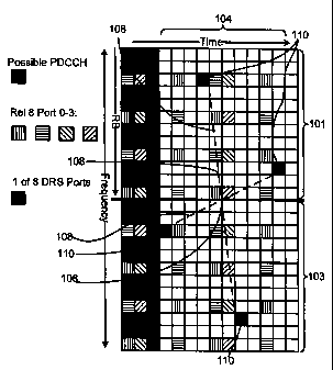
Figs. 5a and 5b, PDSCH 104 has a center at 106. Lines 108 extend between
center-
symmetrically distributed REs 110 of the DRS in RBs 101 and 103. The crossing
point
for each of lines 108 indicates a center of symmetry for the DRS pattern
formed across
RBs 101 and 103. Because lines 108 each cross at center region 106, the
distribution of
DRS REs 110 amongst RBs 101 and 103 is center symmetric. For example, the
position
of each RE in RB 103 may be a point reflection with respect to center point
106 of each
RE in RB 103. In other words, each DRS RE in RB 103 may be positioned by a 180
rotation around center point 106 from each DRS RE in RB 101. As can be seen in
Figs.
5a and 5b, REs 110 are not positioned above one another. As a result, REs 110
are
distributed to different OFDM symbols in time.
11
CA 02766062 2011-12-19
WO 2010/148402 PCT/US2010/039368
[0057] In another implementation of the present system, all DRS REs in an OFDM
symbol of one RB may be center-symmetrically mapped to an adjacent RB as a
group.
This type of mapping can also be realized by reflecting a first RB pattern
about a center
line of the RB (in these examples, the center line denotes the center of the
PDSCH of the
RB). For example, Fig. 6 illustrates a DRS pattern wherein the DRS REs in one
OFDM
symbol of an RB are center-symmetrically mapped to an adjacent RB. In Fig. 6,
center
line 126 indicates a center of the PDSCHs of RBs 122 and 124 with respect to
time. In
this example, DRS REs in OFDM symbol group 120 in RB 122 are reflected about
center
line 126 in RB 124. When constructing RB 124, therefore, the position of each
OFDM
symbol group in RB 124 is determined by the position of each OFDM symbol group
within
RB 122. Each collection of REs included within an OFDM symbol grouping of RB
122 is
reflected directly across line 126 to be positioned within RB 124.
Accordingly, the point of
symmetry of the OFDM symbol groupings in both RB 122 and 124 combined lies at
an
approximate center 130 of the PDSCH regions of RBs 122 and 124.
[0058] Alternatively, rather than reflect each OFDM symbol grouping
independently,
all DRS REs in one half of a first RB may be center-symmetrically mapped to an
adjacent
RB as a group in a second RB. Fig. 7 illustrates a reference signal
configuration where
each RB is split into two groupings, and each grouping is center-symmetrically
mapped to
an adjacent RB by reflection across a center line of the RBs. For example, the
PDSCH
region 152 of RB 154 is separated into two groupings 150 and 152. When
constructing
RB 156, the DRS REs from group 150 are center-symmetrically mapped onto RB 156
by
reflection across a center line of RB 154. Accordingly, grouping 150, which
occupied the
left half of the PDSCH region 152 of RB 154 occupies the right half of the
PDSCH region
152 of RB 156 when center-symmetrically mapped onto RB 156. A similar
algorithm
determines the positioning of grouping 152. As shown by point 158, the center
point of
groupings 150 and 152 is located at the approximate geometrical center of RBs
154 and
156 combined.
[0059] The example DRS patterns described above focus primarily on the
construction of reference signals in pairs of RBs. The reference signal
algorithms
described above, however, may be extended to more than 2 consecutive RBs. In
one
embodiment, for an even number of contiguous RBs, the twin DRS patterns
described
12
CA 02766062 2011-12-19
WO 2010/148402 PCT/US2010/039368
above may be repeated from a first two contiguous RBs into additional
contiguous RBs.
When extending the DRS patterns as described in the present system, any two
contiguous RBs may be configured to have a center-symmetric DRS pattern
structure. In
another embodiment, for an odd number or any number of contiguous RBs, each of
two
different patterns selected from the DRS patterns above may be allocated
alternatively.
The DRS pattern chosen for the first allocated RB to the UA can be derived
from the RB
index.
[0060] Figs. 8a and 8b are illustrations of DRS patterns using the twin DRS
patterns
illustrated in Figs. 5-7 as applied to multiple (more than 2) RBs. In Fig. 8a,
3 RBs 180,
182 and 184 are shown. In RB 180, two example DRS REs are shown as the DRS of
one of 8 antenna ports. In RB 182, REs 196 of RB 180 are reflected by a center
point of
the RB pair 180 and 182. As a result, and as shown by center point 194, REs
196 are
center-symmetrically mapped across RBs 180 and 182.
[0061] Similarly, the REs 196 in RB 184 are center-symmetrically mapped from
the
RE 196 positions in RB 182. To generate the DRS pattern in RB 184, the REs 196
of RB
182 are again reflected by a center point of the RB pair 182 and 184. As a
result, and as
shown by center point 198, REs 196 are center-symmetrically mapped across RBs
182
and 184.
[0062] Fig. 8b illustrates a similar algorithm for constructing the DRS
pattern of RBs
186, 188, 190 and 192. Moving through each RB, the REs of the DRS in the
preceding
RB are reflected across a center point of the RB pair consists of the
preceding RB and
the next RB. As a result, the REs in any pair of RBs are center-symmetrically
mapped to
one another as indicated by center points 200. Alternatively, as Fig. 8b
includes an even
number of RBs, the resulting DRS pattern is constructed by duplicating RB pair
182 and
186 to RB pair 190 and 192.
[0063] Note that the examples shown in Figs. 8a and 8b may be duplicated for a
plurality of RBs that are contiguous over the time domain. In that case, the
DRS REs
may be reflected across a center line of each RB, with the center line being a
center of
the RBs with respect to frequency.
[0064] In a general application of the above examples, for NResCH resource
blocks
assigned to a UA having an index np,B =0,1,...,N S"H -1, reference signal
locations for
13
CA 02766062 2011-12-19
WO 2010/148402 PCT/US2010/039368
each antenna port can be derived from the reference signal locations for
corresponding
antenna ports in the first of the assigned resource blocks for the UA. In one
embodiment,
the reference signal locations in the first of the assigned RB for the UA can
be derived
from the physical index of the RB with a subframe. Given reference symbol
location
(k,l)(P) at sub carrier k and OFDM symbol 1 for antenna port p defined in the
first RB,
nPRB =0, reference signal locations {k',l')(P) for the subsequent RBs can be
derived
according to the following equations:
{nPRBN+ k if nPRR mod 2 = 0 [0065] k' = 2fl],p R -k-1 if nP,mmod2 =1 E q (1)
1 if nPRBmod2 = 0 Eq (2)
[0066] 1' = ND Ls'-' - l + 1 if nPRmod2 =1
[0067] where N b is the number of OFDM symbols in a downlink subframe, NS is
the resource block size in the frequency domain, expressed as a number of
subcarriers.
Eq(1) and Eq(2) may apply to twin RB DRS patterns with any number of
contiguous RBs
in the frequency domain, including those pattern configurations described
above.
10068] Although twin DRS patterns may be derived from any DRS pattern for a
single
RB (for example, by reflecting each RE by a center point of RB pair from the
first RB into
the second RB), certain DRS patterns for a single RB may be preferred for
constructing
twin DRS patterns. For example, in twin DRS patterns, each DRS pattern of a
single RB
should be eligible for transmission in isolation from other RBs. Also, REs for
each
antenna port may be evenly distributed in both the single RB DRS pattern and
the twin
RB DRS pattern.
[0069] Figs. 9a and 9b and Figs. 10a and 10b illustrate reference signal
patterns that
are configured to be transmitted in isolation (as a single RB) or in
combination with other
RBs. The REs in each RB are evenly distributed in both the single RB DRS
pattern and
the combination, or twin, RB DRS patterns of two RBs.
14
CA 02766062 2011-12-19
WO 2010/148402 PCT/US2010/039368
[0070] For example, Fig. 9a illustrates joint DRS pattern designs for
distribution in a
single RB or in twin RBs. In Fig. 9a, to construct the DRS pattern of RB 216,
the REs of
RB 214 are reflected about a center point of the PDSCH 212 of RB pair 214 and
216. As
a result, and as indicated by center point 214, the REs of the DRS of RB 214
are center-
symmetrically mapped to the REs of the DRS of RB 216. Fig. 9b illustrates a
reference
signal pattern for distribution in a single RB or in twin RBs for 6 layers
with the DRS REs
of the first RB being reflected about a center point of the PDSCH of the RB
pair. Figs.
10a and 10b illustrate similar DRS pattern configurations for a Code-Division
Multiplexing
(CDM) implementation. Fig. 10a illustrates the DRS pattern configurations for
8 layers,
while Fig. 10b illustrates the DRS pattern configurations for 6 layers.
[0071] In some implementations of the present system, DRS pattern
configurations
based upon additional available RBs may be implemented. Too many potential DRS
configurations, however, may introduce significant implementation complexity.
As a
result, a limited number of single RB DRS patterns may be allocated in a
particular
implementation of the present system. Furthermore, in addition to twin DRS
patterns,
triple DRS patterns may improve DRS performance while limiting the additional
implementation complexity.
[0072] Fig. 11 illustrates a triple DRS pattern configuration having three
contiguous
RBs with two edge RBs 220 and 224 and one middle RB 222. The edge RBs 220 and
224 share a first, center symmetrical, DRS pattern, while middle RB 222 has a
second
DRS pattern. The two edge RBs 220 and 224 patterns form a twin DRS pattern as
described above for the twin DRS pattern implementations. The middle RB 222 is
configured to include a complementary pattern to further enhance the overall
channel
estimation quality. For the three RBs 220, 222 and 224, center symmetry is
provided for
the middle RB 222, although center symmetry for the middle RB is not
necessary. In the
example shown in Fig. 11, the DRS pattern in middle RB 222 is configured to
make the
DRS evenly distributed across more OFDM symbols.
[0073] Depending upon the system implementation, DRS patterns may be extended
across more than three RBs. For example, when a number of contiguous RBs
across the
frequency domain is a multiple of 3, the DRS pattern may be repeated for every
3 RBs.
When a number of contiguous RBs is a multiple of 6, two different DRS pattern
CA 02766062 2011-12-19
WO 2010/148402 PCT/US2010/039368
configurations may be applied for different groupings of RBs, for example, by
repeating a
triple DRS pattern every 3 RBs, repeating twin DRS patterns (two edge RBs)
every 2
RBs, or by implementing a combination of triple DRS patterns and twin DRS
patterns.
[0074] In some system implementations, it may be advantageous to provide a
method
for implicitly signaling the DRS pattern that is used for an arbitrary number
of contiguous
(in frequency) RBs. In the following example methods, N is the total number of
contiguously allocated RBs. If N=1, then the system uses a single DRS pattern.
If N=2,
the system uses one twin DRS pattern. If N=3, the system uses one triple DRS
pattern.
When N is greater than or equal to 4, the system may apply the following
rules. If N mod
3 = 0, the system uses N13 triple DRS patterns. If (N -- 1) mod 3 = 0, the
system uses
two twin DRS patterns and (N - 4)/3 triple DRS patterns. Finally, if (N - 2)
mod 3 = 0, the
system uses one twin DRS pattern and (N - 2)/3 triple DRS patterns.
[0075] When applying the rules for implicit signaling, there may be a question
as to
where twin DRS pattern(s) should be located with respect to any triple DRS
patterns. In
one case, each twin DRS pattern may be placed in the outermost two RBs at each
edge
of the resource block allocation for the UA. Alternatively, the twin DRS
pattern may be
placed into the center of the resource block allocation (with the recognition
that the
number of triple DRS patterns may be odd, so a perfectly "central" location
may not
exist). Alternatively, other pre-defined rule(s) for determining the location
of any twin
DRS pattern(s) may be defined.
[0076] In many OFDM system implementations, the RBs allocated to a particular
UA
may be contiguous in both frequency and time (if allocated over multiple
subframes).
When the number of RBs assigned to a UA increases, an improved reference
signal
design may be possible by jointly considering DRS patterns on multiple RBs.
For four
contiguous RBs with two RBs being contiguous in the frequency direction and
two RBs
being contiguous in the time direction, several design options may be derived
from the
DRS pattern of a single RB. First, a twin DRS pattern is derived from the DRS
pattern of
a single RB, either in frequency or in time direction. Second, the twin DRS
pattern is
repeated in the time direction (if the first twin DRS pattern is oriented in
the frequency
direction), or repeated in the frequency direction (if the first twin DRS
pattern is oriented
in time direction).
16
CA 02766062 2011-12-19
WO 2010/148402 PCT/US2010/039368
[0077] Figs. 12a and 12b illustrate DRS patterns wherein the DRS patterns of a
first
RB pair are repeated into RBs that are contiguous in both the frequency and
time
domain. In Fig. 12a, RBs 240 and 242 form twin DRS patterns in the frequency
domain.
As shown by center points 244, each of the DRS REs in RB 240 are center-
symmetrically
mapped to the DRS REs in RB 242. The twin DRS pattern is then repeated across
the
time domain from RBs 240 and 242 on the left, to RBs 241 and 243 on the right.
In
contrast, in Fig. 12b, RBs 246 and 248 form twin DRS patterns in the frequency
domain.
As shown by center points 250, each of the REs in RB 246 are center-
symmetrically
mapped to the REs in RB 248. The twin DRS pattern is then repeated across the
time
domain from RBs 246 and 248 on the top, to RBs 247 and 249 on the bottom.
[0078] Alternatively, rather than duplicate the twin DRS patterns across
multiple RBs
across the time or frequency domains, the twin DRS pattern may be reflected
from a first
pair of RBs to a second pair of RBs. First, a twin DRS pattern is derived from
a DRS
pattern of a single RB, either in the frequency or time direction. Second, the
twin DRS
pattern is reflected in the time direction (if the twin DRS pattern from the
first step is
oriented in the frequency direction), or is reflected in the frequency
direction (if the twin
DRS pattern from the first step is oriented in the time direction).
[0079] Figs. 13a and 13b illustrate DRS patterns wherein the DRS patterns from
a first
pair of RBs are reflected into RBs that are contiguous in both the frequency
and time
domain. In Fig. 13a, RBs 260 and 262 form a twin DRS pattern in the frequency
domain.
The DRS pattern of RBs 260 and 262 is then reflected across the subframe
boundary
264 to form a new twin DRS pattern in RBs 266 and 268. As shown by center
points
270, each of the DRS REs in RB pairs 260/262 and 266/268 are center-
symmetrically
mapped to one another. In Fig. 13b, RBs 272 and 274 form a twin DRS pattern in
the
time domain. The DRS pattern of RBs 272 and 274 is then reflected across the
RB
boundary 276 to form a new twin DRS pattern in RBs 278 and 280. As shown by
center
points 282, each of the REs in RB pairs 272/274 and 276/278 are center-
symmetrically
mapped to one another.
[0080] Alternatively, in the case of four contiguous RBs with two RBs being
contiguous in the frequency direction and two RBs being contiguous in the time
direction,
a single RB DRS pattern may be mapped to the other three RBs by using center
17
CA 02766062 2011-12-19
WO 2010/148402 PCT/US2010/039368
symmetric mapping using reflection across the RB boundaries in both the time
domain
and the frequency domain. The symmetric center is the center of the combined
PDSCH
region (in this example, over all four RBs), which may also include the PDCCH
region of
the RBs. The reflection line in the time domain may be the RB boundary and the
reflection line in frequency domain may be the subframe boundary.
[0081] Fig. 14 illustrates a center symmetric DRS pattern for a combination of
four
contiguous RBs, RB 300, RB 302, RB 304 and RB 306, with two RBs contiguous in
the
frequency domain and two RBs contiguous in the time domain. The DRS patterns
for all
four RBs may be derived from the DRS pattern in any one of the RBs, such as RB
300.
Using the DRS pattern of RB 300, for example, the DRS pattern of RB 302 is the
center
symmetric mapping of RB 300, with the center 308 being the crossing point of
the RB
boundary in the time domain and the sub-frame boundary in the frequency
domain. The
DRS pattern of RB 304 is the reflection of the DRS pattern of RB 300 over the
center line
310 of RBs 300 and 304 in the time domain. The DRS pattern of RB 306 is the
reflection
of the DRS pattern of RB 300 over the center line 312 of RBs 300 and 306 in
the
frequency domain. Using a similar algorithm, the DRS pattern of any one of RB
300, RB
302, RB 304 or RB 306 may be used to determine the DRS pattern for each of the
RBs.
[0082] For an OFDM system, twin DRS patterns or other combinations of DRS
patterns may be configured statically, semi-statically or dynamically. For
static
configurations, no explicit signaling is required between a network access
device and the
UA and the configuration can be defined in system specifications. For semi-
static or
dynamic configuration, however, a proper signaling mechanism may be required.
When
a pattern option for a single RB is selected, there are several mechanisms for
spanning a
single DRS pattern across multiple RBs. Two single RB DRS pattern options for
twin
DRS patterns may be selected. Alternatively, three single RB DRS pattern
options may
be selected, two for twin DRS patterns and another for a complementary DRS
pattern.
Four single RB DRS pattern options may be selected, each being derived from a
single
RB DRS pattern by center symmetric mapping as described above. Finally, five
single
RB options may be selected, four of them being derived from a single RB DRS
pattern by
center symmetric mapping and a fifth being complementary for three contiguous
RBs.
18
CA 02766062 2011-12-19
WO 2010/148402 PCT/US2010/039368
[0083] Alternatively, the DRS patterns for each RB may be generated using
predefined rules, formulas or algorithms known at both the transmitter (e.g.,
access
device) and receiver (e.g., UA). When broadcasting an RB, for example, the
access
device may use a predefined algorithm to derive the DRS pattern before
transmitting the
RB to a UA. When using an algorithm to generate the DRS patterns, the
following
principles may be used to design DRS patterns. The rules to construct the DRS
pattern
should be simple, and the DRS pattern should be evenly distributed in the
frequency-time
grid, particularly regarding overall resource allocation. Scalable DRS
patterns may
include a nested structure. As such, a smaller bandwidth DRS pattern may be
allocated
to the first portion of a larger bandwidth pattern. For example, a two-RB DRS
pattern
may include a single RB pattern plus an extended RB pattern. A three-RB DRS
pattern
may include a two-RB pattern plus an extended RB pattern. Finally, the DRS
pattern
may not necessarily be repeated on each RB boundary.
[0084] Fig. 15 illustrates a multi-RB DRS pattern constructed using a
predefined
algorithm for an 8-antenna system implementation. In the following, the M1MO
transmission layers correspond to the antenna ports illustrated in Fig. 5 in
the DRS case.
Generally, the design rules to construct the DRS pattern of Fig. 15 include
the following.
[0085] First, each antenna port is assigned an index with ascending order. In
Fig. 15
there are 8 antenna ports with indices 1, 2, 3, ... 8. The REs specified for
DRS are
assigned to each antenna port in the order of the indices of the antenna port.
The DRS
REs assignment may go along the time domain first, followed by the frequency
domain,
or vice versa. In Fig. 15, the DRS REs for each of the antenna ports go along
the time
domain first, then along the frequency axis. Accordingly, starting from the
first antenna
port, the DRS runs from left to right at the bottom of RB 320 of Fig. 15. The
DRS for the
next antenna port is then positioned to the right of the previous antenna
port.
Accordingly, across the bottom row of RB 320, DRS REs are assigned to antenna
port 1,
2, 3, and 4. Having reached the end of the row, the next higher row of
available DRS
REs are assigned to antenna port 5, 6, 7, and 8. If there were additional
antenna ports,
the next available DRS REs on the next higher row within RB 320 may be used
for
antenna port having those higher indices. After DRS REs are assigned for each
of the
antenna port indices in the sequence, move to the second or third steps.
19
CA 02766062 2011-12-19
WO 2010/148402 PCT/US2010/039368
[0086] In a second step, if the number of antenna ports (e.g., 8 in Fig. 15)
is equal to
a multiple of the number of OFDM symbols allocated for the DRS in each row of
the RE
grid (e.g., 4 in Fig. 15), after finishing one sequence of indices, the
sequence is left cyclic
shifted by a number to generate a new sequence for the next available DRS REs.
In Fig.
15, therefore, after assigning the DRS REs for antenna port 1-8, the process
starts over
at the next available DRS REs within RB 320. However, the starting antenna
port index
is offset by 1. Accordingly, the third row of DRS REs begins with index 2, and
runs
through indices 3, 4, and 5. Having reached the end of the row, the next
higher row of
available DRS REs are assigned to indices 6, 7, 8, and 1. Accordingly, each
new
antenna port sequence in Fig. 15 is left cyclic shifted by 1. This algorithm
may be
implemented to constantly vary the DRS pattern through RBs 320, 322 and 324 as
shown on Fig. 15. With each new combination of DRS REs for indices 1-8, the
starting
index for each pattern is offset by 1.
[0087] In a third step, if the number of antennas is not equal to a multiple
of the
number of OFDM symbols allocated for RS at each antenna port, the index
sequence
generated in the first step is repeated until all REs for the DMS pattern are
filled. For
example, Fig. 16 illustrates a multi-RB DRS pattern constructed using a
predefined
algorithm for a 7-antenna port case. In Fig. 16 there are 7 antenna ports with
indexes 1,
2, 3, ... 7. In Fig. 16, the REs that make up the DRS in each RB are allocated
in the
order of the antenna indices. The assignment may go along the time domain
first,
followed by the frequency domain, or vice versa. In Fig. 16, starting at the
bottom of RB
330 the available DRS REs are allocated to each antenna port index in order.
Accordingly, across the bottom row of RB 330, DRS REs are defined for antenna
port 1,
2, 3, and 4. Having reached the end of the row, the next higher row of
available DRS
REs are assigned to antenna ports 5, 6, and 7.
[0088] Because all the available DRS REs have not been used on the second row
of
the RE grid of RB 330, the next sequence of antenna ports begins immediately
following
the DRS RE for antenna port 7. Accordingly, the second row of available DRS
REs ends
with antenna port 1. Having reached the end of the row, the next higher
antenna port of
available DRS REs are assigned to antenna port 2, 3, 4, and 5. Again, having
reached
the end of the row the next higher row of available DRS REs are assigned to
antenna
CA 02766062 2011-12-19
WO 2010/148402 PCT/US2010/039368
port 6, 7, 1, and 2. Accordingly, each new antenna port sequence in Fig. 16
begins
immediately following the end DRS RE for the prior DRS sequence. The algorithm
may
be implemented to constantly vary the DRS pattern through RBs 330, 332 and
334. As
an example, Fig. 17 illustrates a multi-RB DRS pattern constructed using the
same
predefined algorithm for a 6-antenna port case as was implemented for the 7-
antenna
port case of Fig. 16.
[0089] In some cases, the DRS pattern algorithm illustrated in Figs. 15-17 may
be
summarized as follows and as illustrated in Fig. 18. In step 400, a number of
REs and
the location of each RE within a RB that are available for a DRS pattern are
specified.
The available REs may be arranged on a grid which takes N OFDM symbols in the
time
domain and M subcarriers in the frequency domain. For example, 24 REs for a
DRS
pattern may be specified in an RB.
[0090] In step 402, the number of antenna ports is specified, and the number
of REs
for each antenna port may be derived from the number of antenna ports and
total number
of REs as defined in step 400. For example, a total of 8 antenna ports over 24
REs
would provide up to 3 RE per antenna ports in the DRS pattern of each RB.
[0091] In step 404, DMS REs for each antenna port are assigned following a
predefined sequence, S. The assignment may go along the time domain first
followed by
the frequency domain. For example, Fig. 19 illustrates a plurality of REs 452
allocated
for a DRS pattern within RB 450. As shown in Fig. 19, the assignment starts
from the
leftmost RE on the first row of the grid and continues along the time
direction by
assigning the antenna ports in the sequence, S, to each RE on the RB grid. If
the end of
the grid is reached, the assignment restarts from the leftmost RE on the next
row and
continues. Such assignment continues until all the antenna ports in the
sequence are
exhausted at decision block 405.
[0092] In step 406, if the sequence in step 404 is exhausted at the rightmost
RE in a
row, a new sequence S may be generated by cyclic shifting of the previous
sequence by
one or another integer, as illustrated in Fig. 15. The assignment and sequence
generation process may be repeated until each RE for the DRS pattern in a RB
is
assigned to an antenna port.
21
CA 02766062 2011-12-19
WO 2010/148402 PCT/US2010/039368
[0093] Conversely, in step 408, if the sequence in step 404 is exhausted at an
RE
which is not located at the end of a row, a new sequence S could be generated
by
repeating the previous sequence (as illustrated in Figs. 16 and 17) or by
cyclic shifting
the previous sequence by one or another integer. Such an assignment and
sequence
generation process may be repeated until all REs for DRS in a RB are assigned
to an
antenna port.
[0094] In step 410, in the case of multiple contiguous RBs being allocated,
the above
assignment steps may be carried out continuously across RBs until each RE for
the DRS
pattern in all RBs is assigned with an antenna port (as illustrated in Figs.
15-17).
[0095] Fig. 20 illustrates a wireless communications system including an
embodiment
of UA 10. UA 10 is operable for implementing aspects of the disclosure, but
the
disclosure should not be limited to these implementations. Though illustrated
as a mobile
phone, the UA 10 may take various forms including a wireless handset, a pager,
a
personal digital assistant (PDA), a portable computer, a tablet computer, a
laptop
computer. Many suitable devices combine some or all of these functions. In
some
embodiments of the disclosure, the UA 10 is not a general purpose computing
device like
a portable, laptop or tablet computer, but rather is a special-purpose
communications
device such as a mobile phone, a wireless handset, a pager, a PDA, or a
telecommunications device installed in a vehicle. The UA 10 may also be a
device,
include a device, or be included in a device that has similar capabilities but
that is not
transportable, such as a desktop computer, a set-top box, or a network node.
The UA 10
may support specialized activities such as gaming, inventory control, job
control, and/or
task management functions, and so on.
[0096] The UA 10 includes a display 702. The UA 10 also includes a touch-
sensitive
surface, a keyboard or other input keys generally referred as 704 for input by
a user. The
keyboard may be a full or reduced alphanumeric keyboard such as QWERTY,
Dvorak,
AZERTY, and sequential types, or a traditional numeric keypad with alphabet
letters
associated with a telephone keypad. The input keys may include a trackwheel,
an exit or
escape key, a trackball, and other navigational or functional keys, which may
be inwardly
depressed to provide further input function. The UA 10 may present options for
the user
22
CA 02766062 2011-12-19
WO 2010/148402 PCT/US2010/039368
to select, controls for the user to actuate, and/or cursors or other
indicators for the user to
direct.
[0097] The UA 10 may further accept data entry from the user, including
numbers to
dial or various parameter values for configuring the operation of the UA 10.
The UA 10
may further execute one or more software or firmware applications in response
to user
commands. These applications may configure the UA 10 to perform various
customized
functions in response to user interaction. Additionally, the UA 10 may be
programmed
and/or configured over-the-air, for example from a wireless base station, a
wireless
access point, or a peer UA 10.
[0098] Among the various applications executable by the UA 10 are a web
browser,
which enables the display 702 to show a web page. The web page may be obtained
via
wireless communications with a wireless network access node, a cell tower, a
peer UA
10, or any other wireless communication network or system 700. The network 700
is
coupled to a wired network 708, such as the Internet. Via the wireless link
and the wired
network, the UA 10 has access to information on various servers, such as a
server 710.
The server 710 may provide content that may be shown on the display 702.
Alternately,
the UA 10 may access the network 700 through a peer UA 10 acting as an
intermediary,
in a relay type or hop type of connection.
[0099] Fig. 21 shows a block diagram of the UA 10. While a variety of known
components of UAs 110 are depicted, in an embodiment a subset of the listed
components and/or additional components not listed may be included in the UA
10. The
UA 10 includes a digital signal processor (DSP) 802 and a memory 804. As
shown, the
UA 10 may further include an antenna and front end unit 806, a radio frequency
(RF)
transceiver 808, an analog baseband processing unit 810, a microphone 812, an
earpiece speaker 814, a headset port 816, an input/output interface 818, a
removable
memory card 820, a universal serial bus (USB) port 822, a short range wireless
communication sub-system 824, an alert 826, a keypad 828, a liquid crystal
display
(LCD), which may include a touch sensitive surface 830, an LCD controller 832,
a
charge-coupled device (CCD) camera 834, a camera controller 836, and a global
positioning system (GPS) sensor 838. In an embodiment, the UA 10 may include
another kind of display that does not provide a touch sensitive screen. In an
23
CA 02766062 2011-12-19
WO 2010/148402 PCT/US2010/039368
embodiment, the DSP 802 may communicate directly with the memory 804 without
passing through the input/output interface 818.
[00100] The DSP 802 or some other form of controller or central processing
unit
operates to control the various components of the UA 10 in accordance with
embedded
software or firmware stored in memory 804 or stored in memory contained within
the
DSP 802 itself. In addition to the embedded software or firmware, the DSP 802
may
execute other applications stored in the memory 804 or made available via
information
carrier media such as portable data storage media like the removable memory
card 820
or via wired or wireless network communications. The application software may
comprise a compiled set of machine-readable instructions that configure the
DSP 802 to
provide the desired functionality, or the application software may be high-
level software
instructions to be processed by an interpreter or compiler to indirectly
configure the DSP
802.
[00101] The antenna and front end unit 806 may be provided to convert between
wireless signals and electrical signals, enabling the UA 10 to send and
receive
information from a cellular network or some other available wireless
communications
network or from a peer UA 10. In an embodiment, the antenna and front end unit
806
may include multiple antennas to support beam forming and/or multiple input
multiple
output (MIMO) operations. As is known to those skilled in the art, MIMO
operations may
provide spatial diversity which can be used to overcome difficult channel
conditions
and/or increase channel throughput. The antenna and front end unit 806 may
include
antenna tuning and/or impedance matching components, RF power amplifiers,
and/or low
noise amplifiers.
[00102] The RF transceiver 808 provides frequency shifting, converting
received RF
signals to baseband and converting baseband transmit signals to RF. In some
descriptions a radio transceiver or RF transceiver may be understood to
include other
signal processing functionality such as modulation/demodulation,
coding/decoding,
interleaving/deinterleaving, spread ing/despreading, inverse fast Fourier
transforming
(IFFT)/fast Fourier transforming (FFT), cyclic prefix appending/removal, and
other signal
processing functions. For the purposes of clarity, the description here
separates the
description of this signal processing from the RF and/or radio stage and
conceptually
24
CA 02766062 2011-12-19
WO 2010/148402 PCT/US2010/039368
allocates that signal processing to the analog baseband processing unit 810
and/or the
DSP 802 or other central processing unit. In some embodiments, the RF
Transceiver
808, portions of the Antenna and Front End 806, and the analog base band
processing
unit 810 may be combined in one or more processing units and/or application
specific
integrated circuits (ASICs).
[00103] The analog base band processing unit 810 may provide various analog
processing of inputs and outputs, for example analog processing of inputs from
the
microphone 812 and the headset 816 and outputs to the earpiece 814 and the
headset
816. To that end, the analog base band processing unit 810 may have ports for
connecting to the built-in microphone 812 and the earpiece speaker 814 that
enable the
UA 10 to be used as a cell phone. The analog base band processing unit 810 may
further include a port for connecting to a headset or other hands-free
microphone and
speaker configuration. The analog base band processing unit 810 may provide
digital-to-
analog conversion in one signal direction and analog-to-digital conversion in
the opposing
signal direction. In some embodiments, at least some of the functionality of
the analog
base band processing unit 810 may be provided by digital processing
components, for
example by the DSP 802 or by other central processing units.
[00104] The DSP 802 may perform modulation/demodulation, coding/decoding,
interleaving/deinterleaving, spread ing/despread ing, inverse fast Fourier
transforming
(IFFT)/fast Fourier transforming (FFT), cyclic prefix appending/removal, and
other signal
processing functions associated with wireless communications. In an
embodiment, for
example in a code division multiple access (CDMA) technology application, for
a
transmitter function the DSP 802 may perform modulation, coding, interleaving,
and
spreading, and for a receiver function the DSP 802 may perform despreading,
deinterleaving, decoding, and demodulation. In another embodiment, for example
in an
orthogonal frequency division multiplex access (OFDMA) technology application,
for the
transmitter function the DSP 802 may perform modulation, coding, interleaving,
inverse
fast Fourier transforming, and cyclic prefix appending, and for a receiver
function the
DSP 802 may perform cyclic prefix removal, fast Fourier transforming,
deinterleaving,
decoding, and demodulation. In other wireless technology applications, yet
other signal
CA 02766062 2011-12-19
WO 2010/148402 PCT/US2010/039368
processing functions and combinations of signal processing functions may be
performed
by the DSP 802.
[00105] The DSP 802 may communicate with a wireless network via the analog
baseband processing unit 810. In some embodiments, the communication may
provide
Internet connectivity, enabling a user to gain access to content on the
Internet and to
send and receive e-mail or text messages. The input/output interface 818
interconnects
the DSP 802 and various memories and interfaces. The memory 804 and the
removable
memory card 820 may provide software and data to configure the operation of
the DSP
802. Among the interfaces may be the USB interface 822 and the short range
wireless
communication sub-system 824. The USB interface 822 may be used to charge the
UA
and may also enable the UA 10 to function as a peripheral device to exchange
information with a personal computer or other computer system. The short range
wireless communication sub-system 824 may include an infrared port, a
Bluetooth
interface, an IEEE 802.11 compliant wireless interface, or any other short
range wireless
communication sub-system, which may enable the UA 10 to communicate wirelessly
with
other nearby mobile devices and/or wireless base stations.
[00106] The input/output interface 818 may further connect the DSP 802 to the
alert
826 that, when triggered, causes the UA 10 to provide a notice to the user,
for example,
by ringing, playing a melody, or vibrating. The alert 826 may serve as a
mechanism for
alerting the user to any of various events such as an incoming call, a new
text message,
and an appointment reminder by silently vibrating, or by playing a specific
pre-assigned
melody for a particular caller.
[00107] The keypad 828 couples to the DSP 802 via the interface 818 to provide
one
mechanism for the user to make selections, enter information, and otherwise
provide
input to the UA 10. The keyboard 828 may be a full or reduced alphanumeric
keyboard
such as QWERTY, Dvorak, AZERTY and sequential types, or a traditional numeric
keypad with alphabet letters associated with a telephone keypad. The input
keys may
include a trackwheel, an exit or escape key, a trackball, and other
navigational or
functional keys, which may be inwardly depressed to provide further input
function.
Another input mechanism may be the LCD 830, which may include touch screen
26
CA 02766062 2011-12-19
WO 2010/148402 PCT/US2010/039368
capability and also display text and/or graphics to the user. The LCD
controller 832
couples the DSP 802 to the LCD 830.
[00108] The CCD camera 834, if equipped, enables the UA 10 to take digital
pictures.
The DSP 802 communicates with the CCD camera 834 via the camera controller
836. In
another embodiment, a camera operating according to a technology other than
Charge
Coupled Device cameras may be employed. The GPS sensor 838 is coupled to the
DSP
802 to decode global positioning system signals, thereby enabling the UA 10 to
determine its position. Various other peripherals may also be included to
provide
additional functions, e.g., radio and television reception.
[00109] Fig. 22 illustrates a software environment 902 that may be implemented
by the
DSP 802. The DSP 802 executes operating system drivers 904 that provide a
platform
from which the rest of the software operates. The operating system drivers 904
provide
drivers for the UA hardware with standardized interfaces that are accessible
to
application software. The operating system drivers 904 include application
management
services ("AMS") 906 that transfer control between applications running on the
UA 10.
Also shown in Fig. 22 are a web browser application 908, a media player
application 910,
and Java applets 912. The web browser application 908 configures the UA 10 to
operate
as a web browser, allowing a user to enter information into forms and select
links to
retrieve and view web pages. The media player application 910 configures the
UA 10 to
retrieve and play audio or audiovisual media. The Java applets 912 configure
the UA 10
to provide games, utilities, and other functionality. A component 914 might
provide
functionality described herein.
[00110] The UA 10, base station 12, and other components described above might
include a processing component that is capable of executing instructions
related to the
actions described above. Fig. 23 illustrates an example of a system 1000 that
includes a
processing component 1010 suitable for implementing one or more embodiments
disclosed herein. In addition to the processor 1010 (which may be referred to
as a
central processor unit (CPU or DSP), the system 1000 might include network
connectivity
devices 1020, random access memory (RAM) 1030, read only memory (ROM) 1040,
secondary storage 1050, and input/output (I/O) devices 1060. In some cases,
some of
these components may not be present or may be combined in various combinations
with
27
CA 02766062 2011-12-19
WO 2010/148402 PCT/US2010/039368
one another or with other components not shown. These components might be
located
in a single physical entity or in more than one physical entity. Any actions
described
herein as being taken by the processor 1010 might be taken by the processor
1010 alone
or by the processor 1010 in conjunction with one or more components shown or
not
shown in the drawing.
[00111] The processor 1010 executes instructions, codes, computer programs, or
scripts that it might access from the network connectivity devices 1020, RAM
1030, ROM
1040, or secondary storage 1050 (which might include various disk-based
systems such
as hard disk, floppy disk, or optical disk). While only one processor 1010 is
shown,
multiple processors may be present. Thus, while instructions may be discussed
as being
executed by a processor, the instructions may be executed simultaneously,
serially, or
otherwise by one or multiple processors. The processor 1010 may be implemented
as
one or more CPU chips.
[00112] The network connectivity devices 1020 may take the form of modems,
modem
banks, Ethernet devices, universal serial bus (USB) interface devices, serial
interfaces,
token ring devices, fiber distributed data interface (FDDI) devices, wireless
local area
network (WLAN) devices, radio transceiver devices such as code division
multiple access
(CDMA) devices, global system for mobile communications (GSM) radio
transceiver
devices, worldwide interoperability for microwave access (WiMAX) devices,
and/or other
well-known devices for connecting to networks. These network connectivity
devices
1020 may enable the processor 1010 to communicate with the Internet or one or
more
telecommunications networks or other networks from which the processor 1010
might
receive information or to which the processor 1010 might output information.
[00113] The network connectivity devices 1020 might also include one or more
transceiver components 1025 capable of transmitting and/or receiving data
wirelessly in
the form of electromagnetic waves, such as radio frequency signals or
microwave
frequency signals. Alternatively, the data may propagate in or on the surface
of electrical
conductors, in coaxial cables, in waveguides, in optical media such as optical
fiber, or in
other media. The transceiver component 1025 might include separate receiving
and
transmitting units or a single transceiver. Information transmitted or
received by the
transceiver 1025 may include data that has been processed by the processor
1010 or
28
CA 02766062 2011-12-19
WO 2010/148402 PCT/US2010/039368
instructions that are to be executed by processor 1010. Such information may
be
received from and outputted to a network in the form, for example, of a
computer data
baseband signal or signal embodied in a carrier wave. The data may be ordered
according to different sequences as may be desirable for either processing or
generating
the data or transmitting or receiving the data. The baseband signal, the
signal embedded
in the carrier wave, or other types of signals currently used or hereafter
developed may
be referred to as the transmission medium and may be generated according to
several
methods well known to one skilled in the art.
[00114] The RAM 1030 might be used to store volatile data and perhaps to store
instructions that are executed by the processor 1010. The ROM 1040 is a non-
volatile
memory device that typically has a smaller memory capacity than the memory
capacity of
the secondary storage 1050. ROM 1040 might be used to store instructions and
perhaps
data that are read during execution of the instructions. Access to both RAM
1030 and
ROM 1040 is typically faster than to secondary storage 1050. The secondary
storage
1050 is typically comprised of one or more disk drives or tape drives and
might be used
for non-volatile storage of data or as an over-flow data storage device if RAM
1030 is not
large enough to hold all working data. Secondary storage 1050 may be used to
store
programs that are loaded into RAM 1030 when such programs are selected for
execution.
[00115] The 110 devices 1060 may include liquid crystal displays (LCDs), touch
screen
displays, keyboards, keypads, switches, dials, mice, track balls, voice
recognizers, card
readers, paper tape readers, printers, video monitors, or other well-known
input/output
devices. Also, the transceiver 1025 might be considered to be a component of
the I/O
devices 1060 instead of or in addition to being a component of the network
connectivity
devices 1020. Some or all of the I/O devices 1060 may be substantially similar
to various
components depicted in the previously described drawing of the UA 10, such as
the
display 702 and the input 704.
[00116] The following 3rd Generation Partnership Project (3GPP) Technical
Specifications (TS) are incorporated herein by reference: TS 36.321, TS
36.331, and TS
36.300, TS 36.211, TS 36.212 and TS 36.213.
29
CA 02766062 2011-12-19
WO 2010/148402 PCT/US2010/039368
[00117] While several embodiments have been provided in the present
disclosure, it
should be understood that the disclosed systems and methods may be embodied in
many other specific forms without departing from the spirit or scope of the
present
disclosure. The present examples are to be considered as illustrative and not
restrictive,
and the intention is not to be limited to the details given herein. For
example, the various
elements or components may be combined or integrated in another system or
certain
features may be omitted, or not implemented.
[00118] Also, techniques, systems, subsystems and methods described and
illustrated
in the various embodiments as discrete or separate may be combined or
integrated with
other systems, modules, techniques, or methods without departing from the
scope of the
present disclosure. Other items shown or discussed as coupled or directly
coupled or
communicating with each other may be indirectly coupled or communicating
through
some interface, device, or intermediate component, whether electrically,
mechanically, or
otherwise. Other examples of changes, substitutions, and alterations are
ascertainable
by one skilled in the art and may be made without departing from the spirit
and scope
disclosed herein.
[00119] Thus, it should be appreciated that in a system consistent with the
above
comments, after a single RB DRS pattern has been specified, the single RB DRS
pattern
can be used to derive a DRS pattern for a plurality of contiguous RBs that are
assigned
to a single user agent (UA) wherein the DRS pattern for each adjacent pair of
RBs in the
plurality is different. From the perspective of a UA, the UA can be programmed
to, based
on the number of contiguous RBs assigned to the UA, determine the DRS pattern
used
for contiguous RBs. In some cases, the UA may maintain DRS patterns for
different
numbers of contiguous RBs in a UA memory for easy access.
[00120] To apprise the public of the scope of this invention, the following
claims are
made: