Note: Descriptions are shown in the official language in which they were submitted.
CA 02766981 2011-12-29 110490:911036
DESCRIPTION
TITLE OF INVENTION
Silicon Carbide Insulating Gate Type Semiconductor Device and Fabrication
Method Thereof
TECHNICAL FIELD
The present invention relates to an insulating gate type semiconductor device
employing silicon carbide (SiC) as the semiconductor material, and a method of
fabricating an insulating gate type semiconductor device.
BACKGROUND ART
Recently, SiC is attracting attention as the semiconductor material for the
next
generation. SiC has a dielectric breakdown field of 6MV/cm that is
approximately
one order of magnitude greater than that of silicon (Si). This high dielectric
breakdown property of SiC may provide favorable characteristics for a
semiconductor -
device that could not be realized with Si type semiconductor devices that are
the present
mainstream. Particularly the high breakdown voltage and low loss of SiC
semiconductor devices lead to the strong demand for practical use of realizing
power
conversion devices such as small and highly-efficient inverters and converters
in the
field of electric power, trains, vehicles, electrical appliance and the like.
As such a SiC semiconductor device, there is proposed an insulating gate type
semiconductor device, particularly a vertical MOSFET (MOS Field Effect
Transistor;
metal-oxide film-semiconductor field effect transistor) of the DMOS (Double
Diffused
Metal Oxide Semiconductor) structure (refer to Patent No. 3498459 (Patent
Literature
1)). According to Patent Literature 1, the vertical MOSFET includes a p base
(body)
region, an n+ source region, and an n+ drain region made of silicon carbide; a
gate
insulating film formed at the surface of the p base region, a gate electrode
provided on
the gate insulating film, and two main electrodes for current flow. The
current
between the main electrodes is controlled by applying positive voltage to the
gate
-1-
CA 02766981 2011-12-29 110490:911036
electrode and adjusting the concentration of electrons in the inversion layer
induced at
the surface layer of the p base region located below the gate insulating film.
CITATION LIST
PATENT LITERATURE
PTL 1: Japanese Patent No. 3498459
SUMMARY OF INVENTION
TECHNICAL PROBLEM
A vertical type MOSFET device of the DMOS structure is formed of a plurality
of basic cells, each functioning as a MOSFET of the DMOS structure. Adjacent
basic
cells are arranged so as to form contact at the boundary. Basic cells in the
device
surrounded by basic cells affect each other and exhibit the same behavior.
However
the basic cell located at the outermost circumference (termination section)
receives a
different effect from the surrounding, so that its behavior differs from that
of an interior
basic cell. Particularly, the electric field is concentrated at a portion of
the base (body)
region in an OFF state where current between the main electrodes does not
flow,
leading to the problem of degradation in the breakdown voltage of the device.
In view
of such a problem occurring at the termination section configuration, the
configuration
of the termination section was evaluated and optimized to realize a silicon
carbide
insulating gate type semiconductor device of the present invention having high
breakdown voltage and high performance.
SOLUTION TO PROBLEM
A silicon carbide insulating gate type semiconductor device of the present
invention includes a semiconductor layer of a first conductivity type formed
on a
substrate, and having a first main face opposite to a side of a face in
contact with the
substrate, and an electrode and interconnection formed on the first main face.
The
semiconductor layer includes an active region formed so as to include the
first main
face, and a circumferential resurf region formed in a strip so as to surround
the
circumference of the active region and to include the first main face. In the
active
-2-
CA 02766981 2011-12-29 110490:911036
region, a plurality of basic cells surrounded by an imaginary boundary line
constituting
a polygon in plan view are arranged with no gap so as to form contact at the
boundary
line. Each of the plurality of basic cells has a body region of a second
conductivity
type constituting substantially an analogue to the polygon at the main face.
The
circumferential resurf region is of the second conductivity type, formed to
include the
body region in the basic cells constituting the outermost circumference of the
active
region. The width of a portion of the circumferential resurf region, excluding
the body
region, is greater than or equal to 1/2 the thickness of at least the
semiconductor layer.
According to the present invention, the circumferential resurf region serves
to
alleviate the electric field concentrated at a portion of the body region
located at the
outermost circumference, allowing the breakdown voltage of the silicon carbide
insulating gate type semiconductor device to be improved.
The average impurity concentration of the second conductivity type
circumferential resurf region is preferably higher than, more preferably
greater than or
equal to three times, the average impurity concentration of the second
conductivity type
body region, at the surface region of the semiconductor layer as far as a
depth of 0.05
m from the first main face.
The average impurity concentration of the surface region in the body region
closely relates to the electric property such as the threshold voltage and
channel
mobility of the silicon carbide insulating gate type semiconductor device, and
is in the
vicinity of 1 x 10¹⁶Cm 3, particularly approximately 2 x 1016cm 3. If the
average
impurity concentration of the surface region in the circumferential resurf
region is lower
than the average impurity concentration of the surface region in the body
region, the
surface layer in the body region will be depleted when the silicon carbide
insulating
gate type semiconductor device is in an OFF state, rendering the transition of
the silicon
carbide insulating gate type semiconductor device to an ON state unstable. By
setting
the average impurity concentration of the surface region in the
circumferential resurf
region higher than that of the body region, the introduction of a depletion
layer to the
-3-
CA 02766981 2011-12-29 110490:911036
surface region in the body region is prevented, allowing stable transition to
an ON state.
The body region has an impurity concentration distribution of the second
conductivity type with a maximal value in the depth direction from the first
main face.
At the depth corresponding to the maximal value in the body region, the
impurity
concentration of the second conductivity type in the circumferential resurf
region is
preferably less than or equal to 1 /3 the maximal value of the impurity
concentration of
second conductivity type in the body region. Further, the depth of the
circumferential
resurf region from the first main face is preferably greater than the depth of
the body
region from the first main face.
Accordingly, concentration of the electric field at a portion of the body
region
no longer occurs. The circumferential resurf region functions sufficiently as
an
electric field alleviation layer, leading to improvement of the breakdown
voltage of the
silicon carbide insulating gate type semiconductor device.
The circumferential resurf region is of the p type conductivity, preferably -
including boron for the impurity species. In the case of silicon carbide,
aluminum and
boron can be cited as p type impurities. Boron has an ion implantation range
greater
than that of aluminum, allowing the formation of a deeper impurity region.
The outer circumference of the circumferential resurf region taking a strip
shape
in plan view constitutes a chamfered quadrangle having the four corners
rounded. The
radius of the circumferential chamfered section is preferably greater than or
equal to the
thickness of the drift semiconductor layer. By rounding the four
circumferential
corners, electric field concentration is alleviated, allowing the breakdown
voltage of the
insulating gate field semiconductor element to be further improved.
At least one or more guard ring having conductivity of the second type
identical
to that of the circumferential resurf region is preferably provided so as to
surround the
circumferential resurf region. Since the guard ring serves to alleviate the
electric field,
the breakdown voltage of the silicon carbide insulating gate type
semiconductor device
can be further improved.
-4-
CA 02766981 2011-12-29 110490:911036
A strip-like gate liner interconnection made of metal is arranged on the
circumferential resurf region with an insulating film thereunder. Preferably,
the gate
liner interconnection is electrically connected to all the gate electrodes of
the basic cells
located at the outermost circumference. By the electrical connection between
the gate
liner interconnection and all the gate electrodes at the outermost
circumference, the gate
resistance as the silicon carbide insulating gate type semiconductor device
can be
reduced, allowing an operation at high frequency.
Substantially right below the gate electrode located at the overlapping region
between the basic cell of the outermost circumference and the circumferential
resurf
region in plan view, an anti-inversion region having an impurity concentration
higher
than that of the body region is preferably formed so as to include the first
main face.
The anti-inversion region has conductivity of the second type. The impurity
concentration thereof is preferably equal to the impurity concentration of the
second
conductivity type contact region. By providing the above-described anti-
inversion
region, formation of an inversion layer at the semiconductor layer surface
substantially
right below the gate electrode is less likely to occur, allowing the breakdown
voltage of
the silicon. carbide insulating gate type semiconductor device to be improved.
The shape of the basic cell set forth above is preferably a hexagon in plan
view.
By this hexagon shape in plan view, the body region formed in the basic cell
similarly
takes an analogue hexagon. Since each vertex angle of the body region will
take an
obtuse angle, the electric field concentration can be reduced, allowing the
breakdown
voltage of the silicon carbide insulating gate type semiconductor device to be
improved.
The first main face is preferably inclined greater than or equal to 50 and
less
than or equal to 65 relative to the [0001] plane. Particularly, the first
main face is
preferably the [03-38] plane. By setting the plane orientation of the first
main face
where an inversion layer is formed in the case where silicon carbide is
employed, the
mobility of electrons in the inversion layer can be increased, allowing a
silicon carbide
insulating gate type semiconductor device of low loss to be realized.
-5-
CA 02766981 2011-12-29 110490:911036
A method of fabricating a silicon carbide insulating gate type semiconductor
device includes the steps of preparing a substrate, forming a mask member for
ion
implantation at the substrate, processing the mask member to a predetermined
shape by
photolithography, and performing ion implantation with the mask member as a
mask.
Preferably, the circumferential resurf region and guard ring are formed
simultaneously.
Simultaneous formation of the circumferential resurf region and guard ring
allows the
fabrication steps of the silicon carbide insulating gate type semiconductor
device to be
simplified.
A method of fabricating a silicon carbide insulating gate type semiconductor
device includes the steps of preparing a substrate, forming a mask member for
ion
implantation at the substrate, processing the mask member to a predetermined
shape by
photolithography, and performing ion implantation with the mask member as a
mask.
Preferably, the contact region and anti-inversion region are formed
simultaneously.
Simultaneous formation of the contact region and anti-inversion region allows
the
fabrication steps of the silicon carbide insulating gate type semiconductor
device to be
simplified.
ADVANTAGEOUS EFFECTS OF INVENTION
According to the silicon carbide insulating gate type semiconductor device of
the present invention set forth above, high breakdown voltage and high
performance are
allowed for a semiconductor device.
BRIEF DESCRIPTION OF DRAWINGS
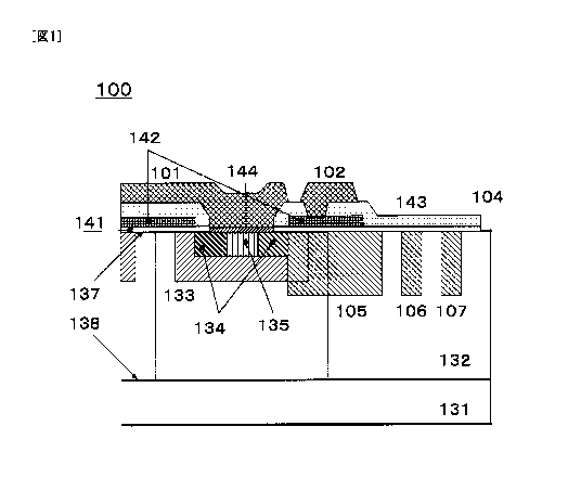
Fig. 1 represents a cross-sectional configuration of a termination section of
a
silicon carbide insulating gate type semiconductor device.
Fig. 2A is a schematic top view representing a schematic plan configuration of
a
silicon carbide insulating gate type semiconductor device.
Fig. 2B represents a schematic plan configuration of a silicon carbide
insulating
gate type semiconductor device, showing an impurity region on a first main
face.
Fig. 3A is a plan view of the first main face corresponding to an enlargement
of
-6-
CA 02766981 2011-12-29 110490:911036
portion A in Fig. 2B of the silicon carbide insulating gate type semiconductor
device,
corresponding to the case where the basic cell takes a quadrangle shape.
Fig. 3B is a plan view of the first main face corresponding to an enlargement
of
portion A in Fig. 2B of the silicon carbide insulating gate type semiconductor
device,
corresponding to the case where the basic cell takes a hexagon shape.
Fig. 4A is a plan view of a first main face of a basic cell configuration of a
silicon carbide insulating gate type semiconductor device, corresponding to
the case
where the basic cell takes a quadrangle shape.
Fig. 4B is a plan view of a first main face of a basic cell configuration of a
silicon carbide insulating gate type semiconductor device, corresponding to
the case
where the basic cell takes a hexagon shape.
Fig. 5 represents a cross-sectional configuration of a basic cell in a silicon
carbide insulating gate type semiconductor device.
Fig. 6 represents a cross-sectional configuration of a termination section in
a
silicon carbide insulating gate type semiconductor device with an anti-
inversion layer
introduced.
Fig. 7 is a flowchart of fabrication steps of a silicon carbide insulating
gate type
semiconductor device.
Fig. 8A is a top view at a point in time when an epitaxial growing step is
completed according to a method of fabricating a silicon carbide insulating
gate type
semiconductor device.
Fig. 8B is a schematic sectional view taken along line VIIIB-VIIIB of Fig. 8A.
Fig. 8C is a top view at a point in time when a body region, a source region,
and
a contact region forming step is completed according to a method of
fabricating a
silicon carbide insulating gate type semiconductor device.
Fig. 8D is a schematic sectional view taken along line VIIID-VIIID of Fig. 8C.
Fig. 8E is a top view at a point in time when a circumferential resurf region
and
guard ring formation step is completed according to a method of fabricating a
silicon
-7-
CA 02766981 2011-12-29 110490:911036
carbide insulating gate type semiconductor device.
Fig. 8F is a schematic sectional view taken along line VIIIF-VIIIF of Fig. 8E.
Fig. 8G is a top view at a point in time when an oxidation step and a gate
electrode formation step are completed according to a method of fabricating a
silicon
carbide insulating gate type semiconductor device.
Fig. 8H is a schematic sectional view taken along line VIIIH-VIIIH of Fig. 8G.
Fig. 81 is a top view at a point in time when an ohmic electrode formation
step
is completed according to a method of fabricating a silicon carbide insulating
gate type
semiconductor device.
Fig. 8J is a schematic sectional view taken along line VIIIJ-VIIIJ of Fig. 81.
Fig. 8K is a top view at a point of time when an interconnection formation
step
is completed according to a method of fabricating a silicon carbide insulating
gate type
semiconductor device.
Fig. 8L is a schematic sectional view taken along line VIIIL-VIIIL of Fig. 8K.
Fig. 9 represents results of impurity distribution in the depth direction
calculated
by Gaussian approximation in a body region formation step of a silicon carbide
insulating gate type semiconductor device.
Fig. 10 represents results of impurity distribution in the depth direction
calculated by Gaussian approximation in a source region formation step of a
silicon
carbide insulating gate type semiconductor device.
Fig. I 1 represents results of impurity distribution in the depth direction
calculated by Gaussian approximation in a contact region formation step of a
silicon
carbide insulating gate type semiconductor device
Fig. 12 represents results of impurity distribution in the depth direction
calculated by Gaussian approximation in a circumferential resurf region
formation step
of a silicon carbide insulating gate type semiconductor device.
Fig. 13A is a sectional view schematically representing a first step in a
method
of forming an impurity region by ion implantation.
-8-
CA 02766981 2011-12-29 110490:911036
Fig. 13B is a sectional view schematically representing a second step in the
method of forming an impurity region by ion implantation.
Fig. 13C is a sectional view schematically representing a third step in the
method of forming an impurity region by ion implantation.
Fig. 13D is a schematic sectional view representing a fourth step in the
method
of forming an impurity region by ion implantation.
Fig. 13E is a schematic sectional view representing a fifth step in the method
of
forming an impurity region by ion implantation.
DESCRIPTION OF EMBODIMENTS
(First Embodiment)
A first embodiment of the present invention will be described in detail
hereinafter with reference to the drawings. In the drawings, the same or
corresponding
elements have the same reference characters allotted, and description thereof
will not be
repeated.
A cross-sectional configuration of a termination section (the section of line
I-I
shown in Figs. 3A and 3B described afterwards) of a silicon carbide insulating
gate type
semiconductor device 100 according to the first embodiment of the present
invention is
shown in Fig. 1. Referring to Fig. 1, the insulating gate type semiconductor
device
according to the present embodiment includes a substrate 131 (support
substrate), a
semiconductor layer 132, a gate oxide film 141, a gate electrode 142, an
interlayer
insulating film 143, an ohmic electrode 144, a source interconnection 101, and
a gate
liner interconnection 102. Semiconductor layer 132 has a first main face 137
and a
second main face 138, opposite to each other. Second main face 138 is in
contact with
substrate 131. Semiconductor layer 132 includes a body region 133, a source
region
134, a contact region 135, a circumferential resurf region 105, and guard
rings 106 and
107, all formed including first main face 137.
Substrate 131 is formed of hexagonal silicon carbide (SiC) having, for
example,
a polytype of 4H. Substrate 131 has conductivity of n+ type, and the thickness
is
-9-
CA 02766981 2011-12-29 110490:911036
approximately 400 m. Although not shown in Fig. 1, a drain electrode is
formed on
the main face of the substrate opposite to the main face in contact with
semiconductor
layer 132. In order to achieve low loss for silicon carbide insulating gate
type
semiconductor device 100, low resistance is desired for substrate 131.
Substrate 131
has an impurity concentration in the range of 5 x 1018cm 3 to 6 x 1019cm 3,
and a
resistivity of approximately 0.5 to 2 mS2=cm. Nitrogen is typical of an n type
impurity.
Although the resistance will become lower as the impurity concentration
becomes
higher, crystallinity will be degraded if the impurity concentration exceeds 6
x 10 19cm 3
The main face of the substrate in contact with second main face 138 of
semiconductor
layer 132 has a plane orientation {00011. More preferably, the off angle
relative to
plane orientation {0001 } is greater than or equal to 50 and less than or
equal to 65 .
For example, plane orientation {03-38} is preferable. In the case where the
main face
of substrate 131 is in the vicinity of plane orientation {03-38}, the plane
orientation of
first main face 137 of semiconductor layer 132 can be set to be in the
vicinity of {03-
38) by forming semiconductor layer 132 on substrate 131 by homoepitaxial
growth.
Semiconductor layer 132 is a SiC layer formed on substrate 131 by epitaxial
growth. Semiconductor layer 132 is closely related to the breakdown voltage of
silicon carbide insulating gate type semiconductor device 100. For example,
when the
breakdown voltage of the device is approximately 1 kV, the n type impurity
concentration is approximately 5 x 1015cm3, and the thickness is approximately
10 m.
Although first main face 137 may have plane orientation {0001 }, first main
face 137
preferably has an off greater than or equal to 50 and less than or equal to
65 relative to
plane orientation {0001 }. For example, first main face 137 has plane
orientation {03-
38}. Such a plane orientation for first main face 137 allows the mobility of
electrons
in the inversion layer formed at channel region 145 in semiconductor layer 132
substantially right below gate electrode 142 that will be described afterwards
to be
increased. Therefore, silicon carbide insulating gate type semiconductor
device 100 is
capable of low loss. Although not shown in Fig. 1, semiconductor layer 132 may
-10-
CA 02766981 2011-12-29 110490:911036
include a buffer layer having a thickness of approximately 0.5 m from second
main
face 138 of semiconductor layer 132, having an n type impurity concentration
of
approximately 5 x 1017cm3.
Body region 133 is formed in semiconductor layer 132 so as to include first
main face 137 of semiconductor layer 132 (refer to Fig. 1). Figs. 4A and 4B
represent
the plan view of each impurity region on first main face 137 of semiconductor
layer 132.
Fig. 4A corresponds to the case where a basic cell 110 takes a quadrangle
shape in plan
view, whereas Fig. 4B corresponds to the case where a basic cell 120 takes a
hexagon
shape in plan view. Referring to Figs. 4A and 4B, body region 133 is
substantially an
analogue to the boundary line (111 or 121) of the basic cell (110 or 120) in
plan view,
and is formed in a basic cell. As an example of the present embodiment, the
ion
implantation condition for the formation of body region 133 and the
distribution of
impurity concentration in the depth direction are shown in Fig. 9 and Table 1,
respectively.
Table 1
First Second Third Fourth Fifth
Ion Species Al Al Al Al Al
Acceleration 35 75 240 400 600
Voltage
e
Dosage /cm 6.0x10 1.3x10 2.5x10 1.0x10 2.0x10
Table 1 represents first to fifth implantations based on the implantation
parameters of implantation species, acceleration voltage (keV) and dosage
(atoms/cm2)
for the ion implantation conditions. In Fig. 9, the impurity concentration
distribution
in the depth direction of each implantation (broken line) and of the sum of
each
implantation (bold solid line) is shown, relative to a depth ( m) taken along
the
horizontal axis with first main face 137a of semiconductor layer 132
corresponding to
the point in time of ion implantation as the origin. In the drawing, the
impurity
concentration of semiconductor layer 132 is indicated by a dotted straight
line 151.
-11-
CA 02766981 2011-12-29 110490:911036
First main face 137a of semiconductor layer 132 corresponding to the point in
time of
ion implantation will be lost by approximately 0.08 m in an oxidation step
that will be
described afterwards. Therefore, first main face 137 of the produced silicon
carbide
insulating gate type semiconductor device 100 is shown in the drawing. With
this first
main face 137 as the origin in Fig. 9, body region 133 of p type conductivity
has an
impurity concentration distribution in the depth direction exhibiting an
average value in
the vicinity of 1 x 1016 cm 3, particularly approximately 2 x 1016 cm 3 at the
surface
region having a depth of 0.05 m from first main face 137. The maximal value
in the
vicinity of 1 x 1018 cm 3 is exhibited at a region deeper than 0.05 m. From
the
crossing position between the bold solid line indicating the impurity
concentration of
the sum of each ion implantation and the dotted straight line 151 indicating
the impurity
concentration of semiconductor layer 132, the depth of body region 133 is
approximately 0.8 m. Since impurity introduction is mainly conducted by ion
implantation and the introduced impurities hardly diffuse in the case of SiC,
it is
difficult to form a deep impurity region. Therefore, in order to ensure the
breakdown
voltage of the device, the total amount of p type impurities in body region
133 must be
set greater than the total amount of impurities in n semiconductor layer 132.
Furthermore, since a channel region 145 is formed at the surface of body
region 133
substantially right below gate electrode 142, the impurity concentration in
the proximity
of the surface of body region 133 must be reduced. Asa result, body region 133
will
have an impurity concentration distribution in the depth direction. Boron (B)
and
aluminum (Al) are typical of p type impurities. Here, Al having a shallow
acceptor
level is employed. This is because the carrier activation is high with a
shallow
acceptor level, allowing an insulating gate type semiconductor device 100 of
low loss to
be realized.
Referring to Figs. 1, 4A and 4B, source region 134 is of n+ type conductivity,
and formed in p type body region 133 in plan view, including first main face
137. As
an example of the present embodiment, the ion implantation conditions to form
source
-12-
CA 02766981 2011-12-29 110490:911036
region 134, and the impurity concentration distribution in the depth direction
are shown
in Table 2 and Fig. 10, respectively.
Table 2
First Second Third
Ion Species P P P
Acceleration Voltage (keV) 90 200 400
Dosage (/cm2) 1 .0 x 1014 2.O x 1014 4.0x10'
4
Table 2 represents first to third implantations based on the implantation
parameters of implantation species, acceleration voltage (keV) and dosage
(atoms/cm2)
for the ion implantation conditions. In Fig. 10, the impurity concentration
distribution
in the depth direction of each implantation (broken line) and of the sum of
each
implantation (bold solid line) is shown, relative to a depth ( m) taken along
the
horizontal axis with first main face 137a of semiconductor layer 132
corresponding to
the point in time of ion implantation as the origin. In the drawing, the
impurity
concentration of body region 133 is indicated by a dotted curve 152. First
main face
137a of semiconductor layer 132 corresponding to the point in time of ion
implantation
will be lost by approximately 0.08 m in an oxidation step that will be
described
afterwards. Therefore, first main face 137 of the produced silicon carbide
insulating
gate type semiconductor device 100 is shown in the drawing. With this first
main face
137 as the origin in Fig. 10, the depth from first main face 137 of source
region 134 is
approximately 0.45 m, from the crossing position between the bold solid line
and the
dotted curve 152. In order to obtain favorable ohmic contact for source region
134,
the impurity concentration of the surface region including first main face 137
is greater
than or equal to 1 X 10¹⁹Cm 3, for example 2 x 1 019cm 3. Although phosphorus
(P) is
employed as the n type impurity in the example of Fig. 10, nitrogen (N) or
arsenic (As)
may be employed.
Referring to Figs. 1, 4A and 4B, contact region 135 is of p+ type
conductivity,
-13-
CA 02766981 2011-12-29 110490:911036
and formed in the p type body region, including first main face 137, so as to
be
surrounded by source region 134 in plan view. The ion implantation conditions
to
form contact region 135, and the impurity concentration distribution in the
depth
direction are shown in Table 3 and Fig. 11, respectively.
Table 3
First Second Third
Ion Species Al Al Al
Acceleration Voltage (keV) 40 110 250
Dosage (/cm) 1.0 X 10¹⁴ 2.O x 10 3.0 X 10
Table 3 represents first to third implantations based on the implantation
parameters of the implantation species, acceleration voltage (keV) and dosage
(atoms/cm2) for the ion implantation conditions. In Fig. 11, the impurity
concentration distribution in the depth direction of each implantation (broken
line) and
of the sum of each implantation (bold solid line) is shown, relative to a
depth ( m)
taken along the horizontal axis with first main face 137a of semiconductor
layer 132
corresponding to the point in time of ion implantation as the origin. In the
drawing,
the impurity concentration of body region 133 is indicated by a dotted curve
153. First
main face 137a of semiconductor layer 132 corresponding to the point in time
of ion
implantation will be lost by approximately 0.08 m in an oxidation step that
will be
described afterwards. Therefore, first main face 137 of the produced silicon
carbide
insulating gate type semiconductor device 100 is shown in the drawing.
Referring to
Fig. 11, the depth from first main face 137 of contact region 135 is
approximately 0.33
m, from the crossing position between the bold solid line and dotted curve 153
in the
drawing. In order to obtain favorable ohmic contact for contact region 135,
the
impurity concentration of the surface region including first main face 137 is
greater
than or equal to 1 X 10¹⁹Cm 3, for example 2 x 1019cm 3. As the p type
impurity, Al or
B may be employed.
-14-
CA 02766981 2011-12-29 110490:911036
Circumferential resurf region 105 is formed in a strip so as to surround
active
region 108 and the circumference of active region 108, and so as to include
first main
face 137. This is shown in Fig. 2B representing a plan view of the entire
appearance
of insulating gate type semiconductor device 100 on first main face 137 of the
semiconductor layer. Figs. 3A and 3B are plan views of the enlargement of A
portion
in Fig. 2B; the former corresponding to a basic cell 110 taking a quadrangle
shape and
the latter corresponding to a basic cell 120 taking a hexagon shape. Referring
to Figs.
3A, 3B, 4A and 4B, a plurality of basic cells (110 or 120) surrounded by an
imaginary
boundary line constituting a polygon in plan view are arranged with no gap, in
contact
with the boundary line (111 or 121) in active region 108. Each of the
plurality of
basic cells (110 or 121) includes a p type body region 133, constituting an
analogue to
the aforementioned polygon at first main face 137. Circumferential resurf
region 105
has a conductivity of the p type, formed to include body region 133 in the
basic cell
(110 or 120) constituting the outermost circumference of active region 108.
The width
d (refer to Figs. 3A and 3B) of circumferential resurf region 105 excluding
body region
133 is greater than or equal to 1/2 the thickness of at least semiconductor
layer 132.
For example, when the breakdown voltage of the device is 1 kV, semiconductor
layer
132 has a thickness of approximately 10 m, and the width d is greater than or
equal to
5 m. Circumferential resurf region 105 formed as set forth above serves to
alleviate
the electric field concentrated at a portion of body region 133 corresponding
to the
outermost circumference, allowing the breakdown voltage of silicon carbide
insulating
gate type semiconductor device 100 to be improved.
Table 4 and Fig. 12 represent the ion implantation condition for formation of
circumferential resurf region 105 and the distribution of the impurity
concentration in
the depth direction, respectively.
-15-
CA 02766981 2011-12-29 110490:911036
Table 4
First Second Third Fourth Fifth Sixth Seventh
Ion Species Al Al Al B B B B
Acceleration
35 75 150 110 200 320 460
Voltage (keV)
Dosage /cm2) 2.5x10¹¹ 6.0x10¹¹ 1.2x10¹² 1.7x10¹² 2.0x10¹² 2.0x10¹² 2.0x10¹²
Table 4 represents first to seventh implantations based on the implantation
parameters of implantation species, acceleration voltage (keV) and dosage
(atoms/cm2)
for the ion implantation conditions. In Fig. 12, the impurity concentration
distribution
in the depth direction of each implantation (broken line) and of the sum of
each
implantation (bold solid line) is shown, relative to a depth ( m) taken along
the
horizontal axis with first main face 137a of semiconductor layer 132
corresponding to
the point in time of ion implantation as the origin. In the drawing, the
impurity
concentration of semiconductor layer 132 is indicated by a dotted straight
line 154.
First main face 137a of semiconductor layer 132 corresponding to the point in
time of
ion implantation will be lost by approximately 0.08 m in an oxidation step
that will be
described afterwards. Therefore, first main face 137 of the produced silicon
carbide
insulating gate type semiconductor device 100 is shown in the drawing.
Referring to
Fig. 12, the impurity concentration of p type circumferential resurf region
105 is
generally about 1 X 1017cm 3. From the crossing position between the bold
solid line
and dotted straight line 154 in the drawing, the depth of circumferential
resurf region
105 from first main face 137 is approximately 1.1 m. Although the
distribution of
impurity concentration in the depth direction of circumferential resurf region
105 is
substantially constant in the present embodiment, the distribution of impurity
concentration in the depth direction of circumferential resurf region 105
satisfies the
relationship set forth below with the distribution of the impurity
concentration of body
region 133 in the depth direction.
First, at the surface region of semiconductor layer 132 up to the depth of
0.05
-16-
CA 02766981 2011-12-29 110490:911036
m into semiconductor layer 132 from first main face 137 of semiconductor layer
132,
the average impurity concentration of body region 133 is in the vicinity of 1
x 1016Cm 3,
particularly about 2 x 1016cm 3 since it is closely related to the electric
property such as
the threshold voltage and channel mobility of silicon carbide insulating gate
type
semiconductor device 100. If the average impurity concentration of
circumferential
resurf region 105 is lower than the average impurity concentration of body
region 133
at the surface region, the surface region of body region 133 is depleted when
insulating
gate type semiconductor device 100 is OFF, rendering the transition of
insulating gate
type semiconductor device 100 to an ON state unstable. By setting the average
impurity concentration of circumferential resurf region 105 higher than that
of body
region 133 at the surface region, introduction of a depletion layer into the
surface region
of body region 133 is prevented, allowing stable transition to an ON state. At
the
surface region, the average impurity concentration of p type circumferential
resurf
region 105 is preferably higher than the average impurity concentration of p
type body
region 133, more preferably at least three times the average impurity
concentration of p
type body region 133. In the examples of Figs. 9 and 12, the average impurity
concentration of circumferential resurf region 105 is approximately 1 x 1017cm
3,
which is about 5 times the average impurity concentration of body region 133
that is
approximately 2 x 1 016cm 3
Secondly, body region 133 has a p type impurity concentration distribution so
as
to exhibit a maximal value, approximately 1 x 1018cm 3 in the example of Fig.
12, in
the depth direction from first main face 137. At the depth of body region 133
corresponding to the maximal value, the p type impurity concentration of
circumferential resurf region 105 is preferably less than or equal to 1 /3 the
maximal
value of the p type impurity concentration of body region 133. With first main
face
137 as the reference in the examples of Figs. 9 and 12, at the depth of
approximately
0.4 m corresponding to the maximal value of p type body region 133, the
impurity
concentration of circumferential resurf region 105 is approximately 1 x 1017cm
3,
-17-
CA 02766981 2011-12-29 110490:911036
which is approximately 1/10 the impurity concentration of body region 133 that
is
approximately 1 x 1018cm 3. The depth of circumferential resurf region 105 is
preferably greater than the depth of body region 133. Accordingly,
concentration of
an electric field at a portion of body region 133 will no longer occur.
Circumferential
resurf region 105 functions sufficiently as an electric field alleviation
layer, allowing
the breakdown voltage of silicon carbide insulating gate type semiconductor
device 100
to be improved. With first main face 137 as the reference in the examples of
Figs. 9
and 12, circumferential resurf region 105 has a depth of 1.1 m, deeper than
the depth
of body region 133 that is 0.8 m.
Although circumferential resurf region 105 is formed deeper than body region
133 in semiconductor layer 132, the deep portion of circumferential resurf
region 105
can be readily realized by using B for the p type impurity species. In the
examples of
Table 4 and Fig. 12, Al is employed as the implantation species in the first
to third
implantations, whereas B is taken as the implantation species for the fourth
to seventh
implantations. This is because the ion implantation range of B is greater than
that of
Al.
Referring to Figs. 3A and 3B, the outer circumference of strip-like
circumferential resurf region 105 in plan view takes a chamfered quadrangle
shape
having the four corners rounded. The radius R of the chamfered section is
preferably
greater than or equal to the thickness of semiconductor layer 132. For
example, when
the breakdown voltage of silicon carbide insulating gate type semiconductor
device 100
is 1 kV, semiconductor layer 132 will have a thickness of approximately 10 m
and a
radius R greater than or equal to 10 m. By virtue of the four corners at the
outer
circumference of circumferential resurf region 105 being rounded, electric
field
concentration is alleviated, allowing the breakdown voltage of silicon carbide
insulating
gate type semiconductor device 100 to be further improved.
Referring to 2B, guard rings 106 and 107 have a p type conductivity identical
to
that of circumferential resurf region 105, formed so as to surround
circumferential
-18-
CA 02766981 2011-12-29 110490:911036
resurf region 105. In the present embodiment, the guard rings are formed
simultaneous to the circumferential resurf region, and have an impurity
concentration
distribution similarly in the depth direction. Preferably, at least one guard
ring is
provided. Fig. 2B corresponds to the case where a first guard ring 106 and a
second
guard ring 107 are provided. Since guard rings 106 and 107 serve to alleviate
the
electric field, the breakdown voltage of silicon carbide insulating gate type
semiconductor device 100 can be further improved.
Insulating gate type semiconductor device 100 of the present embodiment may
further include an anti-inversion region 136. Fig. 6 represents a cross-
sectional
configuration of a termination section in insulating gate type semiconductor
device 100
having anti-inversion region 136 added. Referring to Fig. 6, anti-inversion
region 136
is formed to have an impurity concentration higher than that of body region
133,
including first main face 137, substantially right below gate electrode 142
located at the
overlapping region in plan view between basic cells (110 or 120) located at
the
outermost circumference and the circumferential resurf region. Anti-inversion
region
136 has a p type conductivity, formed simultaneous to p type contact region
135 in the
example of Fig. 6. The impurity concentration in anti-inversion region 136 is
identical
to the impurity concentration in p type contact region 135. By providing anti-
inversion region 136, formation of an inversion layer at the surface region of
semiconductor layer 132 substantially right below gate electrode 142 is less
likely to
occur, allowing the breakdown voltage of silicon carbide insulating gate type
semiconductor device 100 to be improved.
Referring to Fig. 1, gate oxide film 141 is formed on semiconductor layer 132.
Gate oxide film 141 is made of oxide formed by oxidation of SiC, i.e. silicon
dioxide
(SiO2), for example. The thickness of gate oxide film 141 is approximately 40
rim, for
example. Gate electrode 142 is formed on gate oxide film 141 with a desired
plan
arrangement, made of polycrystalline Si into which P is doped in high
concentration,
and has a thickness of approximately 0.5 m. The sheet resistance (the
resistance
-19-
CA 02766981 2011-12-29 110490:911036
value is determined by the vertical and horizontal dimension ratio) of gate
electrode
142 is approximately 10 to 100 mQ/o. Interlayer insulating film 143 is formed
on
gate oxide film 141 and gate electrode 142, made of an oxide of SiO2, and has
a
thickness of approximately 0.6 m. Interlayer insulating film 143 may also be
made
of SiO2 containing approximately several % of P or B, or may be made of
silicon nitride
(SiN). Ohmic electrode 144 is electrically connected to source region 134 and
contact
region 135, and formed on first main face 137 of semiconductor layer 132 so as
to
include contact region 135 and source region 134 of each basic cell (110 or
120).
Ohmic electrode 144 is made of alloy containing titanium (Ti), Al and Si, and
has a
thickness of approximately 0.1 m to 0.2 m. Ohmic electrode 144 realizes a
contact
resistance less than or equal to 1 x 10cm 3 S2cm 2 with respect to contact
region 135
that is of p+ type and source region 134 that is of n+ type. Source
interconnection 101
is electrically connected to all ohmic electrodes 144 in the plurality of
basic cells (110
or 120) constituting active region 108 (refer to Fig. 2B), and is formed on
ohmic
electrode 144 and interlayer insulating film 143, and all over the inner side
of active
region 108 in plan view. Source interconnection 101 is made of metal such as
Al, Al
alloy (including Si, Ti, copper (Cu), and the like), or Cu, and has a
thickness of
approximately 2 to 5 m, depending upon the current capacity of silicon
carbide
insulating gate type semiconductor device 100.
Gate liner interconnection 102 is arranged in a strip on circumferential
resurf
region 105 with interlayer insulating film 143 thereunder, and is made of
metal such as
Al or Al alloy. Gate liner interconnection 102 is preferably connected
electrically to
all gate electrodes 142 of basic cells (110 or 120) located at the outermost
circumference. The electrical connection between gate liner interconnection
102 and
all gate electrodes 142 located at the outermost side allows the gate
resistance of silicon
carbide insulating gate type semiconductor device 100 to be reduced.
Therefore,
operation at high frequency is allowed.
Referring to Figs. 3A, 3B, 4A and 4B, a basic cell (110 or 120) take a polygon
-20-
CA 02766981 2011-12-29 110490:911036
shape surrounded by an imaginary boundary line (111, 121) in plan view. A
plurality
of basic cells are arranged with no gap in active region 108 so as to contact
each other
at the boundary line. The basic cell preferably has a hexagon shape (120) in
plan view.
Accordingly, the body region formed in the basic cell is substantially
analogous to a
hexagon shape. Since each vertex angle of the body region corresponds to an
obtuse
angle, concentration of an electric field is reduced, allowing the breakdown
voltage of
silicon carbide insulating gate type semiconductor device 100 to be improved.
The configuration of gate electrode 142 in plan view will be described
hereinafter with reference to Figs. 3A, 3B, 4A and 4B. In each basic cell (110
or 120),
gate electrode 142 is formed within the imaginary boundary line (111 or 121)
of each
basic cell, and above the region excluding the source region (114 or 124),
with gate
oxide film 141 thereunder. Therefore, gate electrodes 142 are formed
corresponding
to a polygon mesh on active region 108. The formation of gate electrode 142 in
a
mesh-like manner allows, even when one gate electrode 142 is disconnected,
overall
electrical conduction of gate electrodes 142 in silicon carbide insulating
gate type
semiconductor device 100.
The operation of silicon carbide insulating gate type semiconductor device 100
of the present embodiment will be described hereinafter with reference to Fig.
5.
First, an ON state of silicon carbide insulating gate type semiconductor
device
100 will be described. Fig. 5 represents a cross-sectional configuration taken
along
line V-V shown in Figs. 4A and 4B. Referring to Fig. 5, when a voltage higher
than
the threshold voltage with respect to source interconnection 101 is applied to
gate
electrode 142, an inversion layer (a layer of n conductivity type) is formed
at channel
region 145 including first main face 137, in semiconductor layer 132 at p type
body
region 133 located substantially right below gate electrode 142. By this
formation of
an inversion layer, electrical connection with n+ type substrate 131 is
established via n+
type source region 134 and n type semiconductor layer 132. Although not shown
in
Fig. 5, a drain electrode is formed on the main face of substrate 131 opposite
to the
-21-
CA 02766981 2011-12-29 110490:911036
main face in contact with semiconductor layer 132. As a result of formation of
an
inversion layer, current flows across source interconnection 101 and the drain
electrode.
In silicon carbide insulating gate type semiconductor device 100 of the
present
embodiment, first main face 137 of semiconductor layer 132 preferably has a
plane
orientation whose off angle relative to plane orientation {0001 } is greater
than or equal
to 50 and less than or equal to 65 , for example, plane orientation {03-38}.
Accordingly, the formation of an interface state in the proximity of the
interface
between gate oxide film 141 and semiconductor layer 132 at channel region 145
is
suppressed, so that the mobility of electrons in the inversion layer is
improved.
Therefore, a silicon carbide insulating gate type semiconductor device 100 of
low loss
is allowed.
When a voltage less than or equal to the threshold voltage with respect to
source
interconnection 101 is applied to gate electrode 142, or when the potential of
gate
electrode 142 is set equal to the potential of source interconnection 101,
silicon carbide
insulating gate type semiconductor device 100 attains an OFF state, so that
current does
not flow across source interconnection 101 and the drain electrode. This is
because
the inversion layer formed at the channel region 145 is eliminated, so that
source region
134 will not be electrically connected to n type semiconductor layer 132
through p type
body region 133.
In such an OFF state, a depletion layer extends towards each of p type body
region 133 and n type semiconductor layer 132 from the pn junction by p type
body
region 133 and n type semiconductor layer 132. At this stage, the total amount
of p
type impurities in the depletion layer at p type body region 133 is generally
equal to the
total amount of n type impurities in the depletion layer at n type
semiconductor layer
132. Since it is difficult to form a deep impurity region by silicon carbide,
p type body
region 133 must exhibit an impurity concentration distribution in the depth
direction
with a maximum in semiconductor layer 132.
Particularly at the termination section of silicon carbide insulating gate
type
-22-
CA 02766981 2011-12-29 110490:911036
semiconductor device 100 in an OFF state (refer to Fig. 1), it is critical to
provide an
electric field alleviation layer such as by circumferential resurf region 105
and/or guard
rings 106 and 107 since electric field concentration readily occurs at a
portion of body
region 133. In addition, the provision of anti-inversion region 136 (refer to
Fig. 6) is
effective for a stable operation of silicon carbide insulating gate type
semiconductor
device 100. Moreover, by avoiding concentration of electric field by virtue of
the
plurality of basic cells arranged in the active region taking a hexagon shape
in plan
view whose vertex angle is an obtuse angle, the breakdown voltage of silicon
carbide
insulating gate type semiconductor device 100 can be increased.
Moreover, it is critical to reduce the gate resistance when seen from a gate
terminal external to the device for silicon carbide insulating gate type
semiconductor
device 100 to allow high-speed switching or to operate at high frequency. By
electrically connecting the gate electrode included in each of a plurality of
basic cells
located at the outermost circumference with gate liner interconnection 102 in
insulating
gate type semiconductor device 100 of the present embodiment, the gate
resistance is
reduced, allowing high speed operation and high frequency operation.
A method of fabricating an insulating gate type semiconductor device 100 of
the
present embodiment will be described based on the fabrication flow of Fig. 7
as well as
Figs. 8A-8L at a point in time when each step is completed. Referring to Fig.
7,
insulating gate type semiconductor device 100 is fabricated in the sequence of
a
substrate preparation step P1, a semiconductor layer formation step P2, an
impurity
region formation step P3, an activation annealing step P4, an oxidation step
P5, a gate
electrode formation step P6, an interlayer insulating film formation step P7,
an ohmic
electrode formation step P8, an interconnection formation step P9, and a
passivation
step PlO. Figs. 8A-8L represent a plan configuration and a cross-sectional
configuration of an insulating gate type semiconductor device in the
fabrication process.
The fabrication method will be described in detail hereinafter with reference
to Figs.
8A-8L.
-23-
CA 02766981 2011-12-29 110490:911036
At step PI (Fig. 7), substrate 131 is prepared. For example, a substrate 131
made of single crystal silicon carbide having a polytype of 4H, and of n type
conductivity is prepared at step P l. The plane orientation of the main face
of substrate
131 is, for example, {0001 }. More preferably, the main face of substrate 131
has an
off angle greater than or equal to 50 and less than or equal to 65 relative
to plane
orientation {0001), more preferably, has plane orientation {03-38}. Further,
substrate
131 preferably has a low resistivity. Therefore, a substrate having an n type
impurity
concentration of 5 x 1018cm 3 to 6 x 10¹⁹Cm 3, for example, is prepared.
At step P2 (Fig. 7), semiconductor layer 132 is formed on substrate 131.
Specifically, referring to the plan configuration of Fig. 8A and the cross-
sectional
configuration of Fig. 8B, n type semiconductor layer 132 made of silicon
carbide is
formed by epitaxial growth on the main face of substrate 131. Epitaxial growth
is
carried out based on the mixture of SiH4 (silane) and C3H8 (propane) as the
material gas,
further having n type impurities introduced. At this stage, the impurity
concentration
and thickness of semiconductor layer 132 may be adjusted depending upon the
breakdown voltage of the device. For example, when the breakdown voltage of
the
semiconductor device is 1 kV, the n type impurity concentration of
semiconductor layer
132 is approximately 5 x 1015cm3, and the thickness is approximately 10 m.
For the
n type impurity, nitrogen, for example, is employed.
Semiconductor layer 132 includes second main face 138 in contact with
substrate 131, and first main face 13 7a at the opposite side. Since substrate
131 is
made of silicon carbide identical to that of semiconductor layer 132, the
plane
orientation of first main face 137a can be set identical to the plane
orientation of the
main face of the substrate in contact with second main face 138 by means of
homogenous growth. By the main face of the substrate in contact with
semiconductor
layer 132 having a plane orientation whose off angle relative to {0001 } is
greater than
or equal to 50 and less than or equal to 65 , particularly a plane
orientation of {03-38},
first main face 137a of semiconductor layer 132 can be set to have the above-
described
-24-
CA 02766981 2011-12-29 110490:911036
plane orientation. Such a plane orientation for first main face 137a allows
increasing
the mobility of electrons in the inversion layer formed at channel region 145
when
silicon carbide insulating gate type semiconductor device 100 is ON.
Therefore, low
loss of silicon carbide insulating gate type semiconductor device 100 can be
realized.
At step P3 (Fig. 7), an impurity region is formed so as to include first main
face
137a in semiconductor layer 132. Referring to the plan configuration of Fig.
8C and
the cross-sectional configuration of Fig. 8D, body region 133, source region
134, and
contact region 135 are formed by ion implantation in step P3. Referring to the
plan
configuration of Fig. 8E and the cross sectional configuration of Fig. 8F,
circumferential resurf region 105 and guard rings 106 and 107 are formed by
ion
implantation. Then, activation annealing of the introduced impurities is
effected by
thermal treatment. In the case of silicon carbide, impurities hardly diffuse.
It is
difficult to introduce impurities from a gaseous or solid source. Therefore,
impurities
are introduced by ion implantation. An impurity distribution in the depth
direction is
realized by ion implantation carried out over multiple times.
A method of forming an impurity region by ion implantation will be described
specifically hereinafter. First, by step P2 as described above, an epitaxial
substrate
200 including substrate 131 and semiconductor layer 132 with first main face
137a is
prepared (Fig. 13A). Then, on epitaxial substrate 200, i.e. on first main face
137a of
semiconductor layer 132, an oxide film 300 (mask member for ion implantation)
made
of silicon dioxide (Si02) is formed by CVD (Chemical Vapor Deposition), for
example
(Fig. 13B). A resist is applied on oxide film 300, followed by exposure and
developing, to form a resist film 301 having an opening corresponding to the
shape of
each desired impurity region (Fig. 13C). Using resist film 301 as a mask,
oxide film
300 exposed at the opening of resist film 301 is removed by RIE (Reactive Ion
Etching),
for example. Ions are implanted with oxide film 300 and resist film 301 as the
mask,
whereby impurities are introduced into semiconductor layer 132 at the opening
(Fig.
13E). Following ion implantation, resist film 301 and oxide film 303 are
removed by
-25-
CA 02766981 2011-12-29 110490:911036
oxygen plasma ashing and hydrochloric acid based solution, respectively.
Body region 133 of p type conductivity is formed such that the impurity
concentration varies in the depth direction from first main face 137a of
semiconductor
layer 132. Referring to the example in Fig. 9, p type impurities are
introduced over a
depth of approximately 0.9 m. The concentration thereof is approximately 2 x
1016cm3 in the vicinity of the surface up to the depth of 0.15 m, referenced
to first
main face 137a, and has a maximal value of 2 x 1017cm 3 at the depth greater
than or
equal to 0.15 m. For p type impurities, B and Al can be cited. Here, Al
having a
shallow acceptor level is employed. This is because a silicon carbide
insulating gate
type semiconductor device 100 of low loss can be realized since the carriers
have high
activation rate when the acceptor level is shallow. Further, since
semiconductor layer
132 will be partially lost by oxidation step P5 (Fig. 7) that will be
described afterwards,
first main face 137 of semiconductor layer 132 in the produced semiconductor
device
100 is located at the depth of approximately 0.08 m at this stage.
Source region 134 of n type conductivity is formed by ion implantation over
multiple times with P as the n type impurity. For the n type impurity, N or
arsenic
(As) may also be employed. Referring to the example of Fig. 10, a source
region 134
of approximately 0.53 m in depth, having an impurity concentration
distribution in the
depth direction is formed, wherein the n type impurity concentration is
approximately 2
x 1019cm3 in the vicinity of a depth 0.08 m, referenced to first main face
137a.
Contact region 135 of p type conductivity is formed by ion implantation over
multiple times with Al as the p type impurity. For the p type impurity, B may
also be
employed. Referring to the example of Fig. 11, a contact region 135 of
approximately
0.4 m in depth, having an impurity concentration distribution in the depth
direction is
formed, wherein the p type impurity concentration is approximately 2 x 1019cm
3 in the
vicinity of a depth 0.08 m, referenced to first main face 137a.
Since semiconductor layer 132 will be partially lost by oxidation step P5
(Fig.
7) that will be described afterwards, first main face 137 of semiconductor
layer 132
-26-
CA 02766981 2011-12-29 110490:911036
having an ohmic electrode that will be described afterwards formed is located
at the
depth of approximately 0.08 m at this stage. By setting the impurity
concentration at
the depth of approximately 0.08 .tm in the vicinity of approximately 2 x
1019cm 3, a
favorable ohmic contact can be realized.
Circumferential resurf region 105 of p type conductivity is formed by varying
the impurity concentration in the depth direction from first main face 137a of
semiconductor layer 132. Referring to the example of Fig. 12, circumferential
resurf
region 105 of approximately 1.2 pm in depth, having an impurity concentration
distribution in the depth direction is formed, wherein the p type impurity
concentration
is approximately 1 x 1017cm3 in the proximity of the surface down to the depth
of
approximately 0.15 m, referenced to first main face 13 7a, and exhibiting a
maximal
value of 2 x 1017cm3 at the depth greater than or equal to 0.15 m. For the p
type
impurity, B and Al are employed. The shallow portion is made of Al, and the
deep
region is made of B. Since semiconductor layer 132 is partially lost by
oxidation step
P5 (Fig. 7) that will be described afterwards, first main face 137 of
semiconductor layer
132 will be located at the depth of approximately 0.08 m at this stage.
Formation of guard rings 106 and 107 may be carried out simultaneous to the
formation of circumferential resurf region 105 or the formation of contact
region 135.
In the present embodiment, the formation of guard rings 106 and 107 is carried
out
simultaneous to the formation of circumferential resurf region 105. Moreover,
formation of anti-inversion region 136 is carried out simultaneous to the
formation of
contact region 135 in the present embodiment.
In order to render the impurity regions formed by ion implantation such as
body
region 133, source region 134, contact region 135, circumferential resurf
region 105,
and guard rings 106, 107 electrically active, activation annealing step P4
(Fig. 7) is
carried out at one time. At step P4, a thermal treatment maintained at 1700 C
for 30
minutes in an argon gas atmosphere, for example, can be carried out.
Then, the main face of the semiconductor layer is subjected to thermal
oxidation.
-27-
CA 02766981 2011-12-29 110490:911036
At step P5 (Fig. 7), in order to remove the damage (defect) caused by ion
implantation
or the like, present at the surface of first main face 137a of semiconductor
layer 132,
thermal oxidation (sacrificial oxidation) is performed once, followed by
removing the
oxide film produced by the sacrificial oxidation. Then, thermal oxidation is
performed again to form gate oxide film 141. Sacrificial oxidation and gate
oxidation
are both performed by exposing the substrate in the fabrication process in a
dry oxygen
atmosphere for 60 minutes at the temperature of 1300 C, for example. At this
stage,
the thickness of the oxide film produced by one thermal oxidation is
approximately 40
nm. In accordance with the growth (formation) of an oxide film, semiconductor
layer
132 will be consumed by a thickness substantially equal to the thickness of
the oxide
film when silicon carbide is used. Therefore, first main face 137 of the
semiconductor
layer recedes approximately 80 nm (0.08 m) inward of the semiconductor layer,
referenced to first main face 137a prior to the oxidation step.
Referring to the plan configuration of Fig. 8G and the cross-sectional
configuration of Fig. 8H, gate electrode 142 is formed on gate oxide film 141.
At this
step P6 (Fig. 7), a polycrystalline silicon film is formed by LPCVD (Low
Pressure
Chemical Vapor Deposition). This polycrystalline silicon film is etched to a
predetermined configuration by photolithography to form a gate electrode. In
the
LPCVD method, PH3 (phosphine) is introduced as the n type impurity, using
SiH2C12
(dichlorosilane) as the material gas, to form a polycrystalline silicon film
having
impurities doped at the temperature of 1000 C and reduced pressure of 30Pa.
The
polycrystalline silicon film has a thickness of approximately 0.5 m, for
example, and a
sheet resistance of 20 mQ/D. Etching is carried out by RIE using CH4 (freon)
based
gas, for example.
Referring to the plan configuration of Fig. 8A and the cross-sectional
configuration of Fig. 8B, an interlayer insulating film 143 and ohmic
electrode 144 are
formed on gate electrode 142. In the formation step P7 (Fig. 7) of interlayer
insulating
film 143, an SiO2 film is deposited to a thickness of approximately 0.6 m by
CVD, for
-28-
CA 02766981 2011-12-29 110490:911036
example, entirely on the surface of exposed gate electrode 142 of insulating
gate type
semiconductor device 100 in a fabrication process. Interlayer insulating film
143 may
be formed by PCVD (Plasma Chemical Vapor Deposition) instead of CVD.
Interlayer
insulating film 143 may be made of silicon nitride (SiN).
Then, ohmic electrode 144 electrically connecting source region 134 and
contact
region 135 is formed. This ohmic electrode formation step (P8) involves source
region 134 and contact region 135. An opening is formed in gate oxide film 141
and
interlayer insulating film 143 so that first main face 137 of semiconductor
layer 132 is
exposed by photolithography and etching. Then, by electron beam deposition,
titanium (Ti), Al and Si are sequentially deposited to a thickness of 200 nm,
400 nm
and 250 nm, respectively, without removing the resist. Then, the Ti, Al, Si
layers
deposited on the resist are removed together with the resist (the so-called
lift off
method). Then, thermal treatment is carried out for 30 seconds at the
temperature of
approximately 950 C in an inert atmosphere such as of argon (Ar) or N to form
an alloy
layer of the silicon carbide of semiconductor layer 132 and the Ti, Al, Si.
The alloy
layer is taken as ohmic electrode 144.
Referring to the plan configuration of Fig. 8K and the cross-sectional
configuration of Fig. 8L, source interconnection 101 and gate liner
interconnection 102
electrically connected to ohmic electrode 144 in all the basic cells (110 or
120) and the
gate electrode of each of basic cells located at the outermost circumference,
respectively, are formed on interlayer insulating film 143. In this
interconnection
formation step P9 (Fig. 7), all basic cells (110 or 120) located at the
outermost
circumference are subjected to photolithography to have an opening formed in
interlayer insulating film 143 on gate electrode 142 located on
circumferential resurf
region 105. Then, Al or Al alloy is provided by sputtering or the like to a
thickness of
approximately 2-5 gm after removing the resist. The Al or Al alloy is etched
to form
source interconnection 101 and gate liner interconnection 102. The etching of
Al or
Al alloy is allowed by RIE using chlorine (Cl) based gas.
-29-
CA 02766981 2011-12-29 110490:911036
Finally, a protection film of the organic type such as polymide, or such as of
SiO2 or SiN is formed (not shown) to complete silicon carbide insulating gate
type
semiconductor device 100 of the present embodiment.
It is to be understood that the embodiments disclosed herein are only by way
of
example, and not to be taken by way of limitation. The scope of the present
invention
is not limited by the description above, but rather by the terms of the
appended claims,
and is intended to include any modifications within the scope and meaning
equivalent
to the terms of the claims.
REFERENCE SIGNS LIST
100 insulating gate type semiconductor device; 101 source interconnection; 102
gate liner interconnection; 103 gate pad; 104 end face of semiconductor
device; 105
circumferential resurf region; 106 first guard ring; 107 second guard ring;
108 active
region; 110 quadrangle basic cell; 111 imaginary boundary line of quadrangle
basic
cell; 112 body region of quadrangle basic cell; 113 contact region of
quadrangle basic
cell; 114 source region of quadrangle basic cell; 120 hexagon shape basic
cell; 121
imaginary boundary line of hexagon shape basic cell; 122 body region of
hexagon
shape basic cell; 123 contact region of hexagon shape basic cell ; 124 source
region of
hexagon shape basic cell ; 130 cross-sectional configuration of basic cell;
131 substrate;
132 semiconductor layer; 133 body region; 134 source region; 135 contact
region; 136
anti-inversion region; 137 first main face of semiconductor layer; 137a first
main face
of semiconductor layer prior to oxidation step; 138 second main face of
semiconductor
layer; 141 gate oxide film; 142 gate electrode; 143 interlayer insulating
film; 144 ohmic
electrode; 145 channel region; 151 impurity concentration of semiconductor
layer; 152
impurity concentration of body region; 153 impurity concentration of body
region; 154
impurity concentration of semiconductor layer.
-30-