Note: Descriptions are shown in the official language in which they were submitted.
201023835 CA 02767709 2012-02-10
1
Description
Controller for a power converter and method of operating the
same
FIELD OF INVENTION
The present invention relates to the field of power convert-
ers.
BACKGROUND OF THE INVENTION
Within closed loop control systems which use sampled feedback
data there is a finite delay between sampling the feedback
variable and the actuator changing in response to these feed-
back signals. For example, in case of a three phase voltage
sourced converter, the feedback variables are the three phase
currents, and the actuator is in effect the pulse width modu-
lation (PWM) bridge which changes the three phase voltage in
amplitude and phase to control the three phase currents.
Typically in fixed switching frequency PWM schemes the cur-
rent is sampled many times during a complete PWM period (PWM
period = 1/(switching frequency)) and the average taken of
these multiple samples becomes the current feedback variable
as used by a controller. Using this method good attenuation
of the PWM switching frequency related harmonic currents is
achieved. However a finite phase delay is introduced within
the control loop, due to the delay between sampling the cur-
rent, doing the necessary mathematical calculations, and
changing the voltage. Hence the PWM voltage actually changes
in response to this sampled current with a certain delay. It
is desirable from the point of view of control system stabil-
ity, particularly when arrays of network connected PWM
bridges are considered that these phase delays are minimised.
In view of the above-described situation, there exists a need
for an improved technique that enables to provide a converter
201023835 CA 02767709 2012-02-10
2
controller with improved characteristics, while substantially
avoiding or at least reducing one or more of the above-
identified problems.
SUMMARY OF THE INVENTION
This need may be met by the subject matter according to the
independent claims. Advantageous embodiments of the herein
disclosed subject matter are described by the dependent
claims.
According to a first aspect of the invention there is pro-
vided a controller for a converter, the converter receiving
an input power and providing an output power by a switching
operation, the controller comprising: an input for receiving
a feedback signal depending on the output power of the con-
verter; and an output for providing a control signal to the
converter to thereby control the switching operation of the
converter, the control signal corresponding to a switching
pattern that is updated in response to the feedback signal;
the control signal having an harmonic compensation signal
which reduces higher harmonics in the output power, the
higher harmonics originating from a time delay between taking
the feedback signal and the updating of the switching pat-
tern.
This aspect of the invention is based on the idea that a de-
lay between taking of the feedback signal and updating the
switching pattern can be reduced while maintaining undesired
harmonics at an acceptable level by at the same time compen-
sating these harmonics by at least one a harmonic compensa-
tion signal in the control signal to the converter.
According to an embodiment, the converter is a power con-
verter, e.g. a power converter of a wind turbine device.
According to an embodiment, the output power has at least two
phases, e.g. three phases (three-phase power). For example,
201023835 CA 02767709 2012-02-10
3
in an embodiment the output power is provided on two or more
electrical conductors (one for each phase) carrying alternat-
ing currents with a definite time offset (phase difference)
between the voltage waves in each conductor. In other embodi-
ments, the output power has a single phase.
According to an embodiment, the controller further comprises
a modulation signal generator for providing a modulation sig-
nal; a compensation generator for generating a harmonic com-
pensation component; wherein the controller is configured for
providing the control signal depending on the modulation sig-
nal and the harmonic compensation component.
According to an embodiment, the harmonic compensation compo-
nent includes one or more harmonic components of suitable
phase and magnitude to compensate undesired harmonics in the
PWM voltage. Generally herein the harmonic compensation com-
ponent includes a single one of such harmonic components or,
in another embodiment, a plurality of such harmonic compo-
nents (of suitable phase and magnitude).
According to a further embodiment, the controller further
comprises an adder for adding the modulation signal and the
harmonic compensation component to thereby generate a summing
signal. For example, according to an embodiment, the harmonic
compensation component is the harmonic component which is di-
rectly added to the modulation signal. In such a case, the
summing signal is the control signal.
According to another embodiment, the controller further com-
prises a signal processing unit for processing the summing
signal, thereby generating the control signal. For example,
the summing signal may be compared to a reference signal,
e.g. a triangular carrier signal in order to obtain the times
where switching has to occur.
According to a further embodiment, the controller further
comprises a lookup table having stored therein a plurality of
201023835 CA 02767709 2012-02-10
4
compensation indicators, each compensation indicator corre-
sponding to a respective harmonic compensation component; and
the compensation generator being configured for generating
the harmonic compensation component on the basis of a se-
lected compensation indicator. Further, according to an em-
bodiment, the compensation generator is configured for re-
ceiving at least one of a modulation depth, a modulation an-
gle and the time delay; and providing in response hereto the
harmonic compensation component.
For example, in an embodiment the lookup table has stored
therein compensation indicators for a plurality of different
modulation depths, modulation angles and time delays. The
compensation generator is then configured for receiving an
actual modulation depth, a modulation angle and the time de-
lay and for selecting in response hereto the corresponding
compensation indicator. The compensation generator generates
the harmonic compensation component on the basis of the se-
lected compensation indicator.
According to a further embodiment, the output power has at
least two phases and the update of the switching pattern is
performed at a point in time where the voltage levels of the
at least two phases are different. For example, without har-
monic compensation signal an update of the switching pattern
would be performed at a midpoint of a zero vector, wherein
the zero vector corresponds to the time interval where the
voltage level is identical for all of the at least two
phases. Having the harmonic compensation signal according to
embodiments of the herein disclosed subject matter, the up-
date of the switching pattern can be performed at any time,
independent of the midpoint of the zero vector, i.e. in par-
ticular at times where the voltage levels of the at least two
phases are different. An alternative for a "point in time
where the voltage levels of the at least two phases are dif-
ferent" is a point in time where the control signal compo-
nents for each of the at least two phases are different.
201023835 CA 02767709 2012-02-10
According to a further embodiment, the time delay is deter-
mined by a computation time necessary to determine the con-
trol signal. For example, in an embodiment the time delay is
not prolonged artificially but is only determined by the nec-
5 essary computation time. In this sense, such a time delay is
a minimum time delay that is due to the configuration of the
controller.
According to a second aspect of the herein disclosed subject
matter, a converter device is provided, the converter device
comprising a controller according to the first aspect or an
embodiment thereof; and the converter referred to in the
first aspect, the converter having an input for receiving the
input power and an output for providing the output power by
the switching operation.
According to a third aspect of the herein disclosed subject
matter, a method of operating a controller for a converter is
provided, the converter receiving an input power and provid-
ing an output power by a switching operation, the method com-
prising receiving a feedback signal depending on the output
power of the converter; and providing a control signal to the
converter to thereby control the switching operation of the
converter, the control signal corresponding to a switching
pattern that is updated in response to the feedback signal;
the control signal having an harmonic compensation signal
which reduces higher harmonics in the output power, the
higher harmonics originating from a time delay between taking
the feedback signal and the updating of the switching pat-
tern.
According to an embodiment of the third aspect, the output
power has at least two phases.
According to an embodiment of the third aspect, the method
further comprises providing a modulation signal; generating a
harmonic compensation component; and providing the control
201023835 CA 02767709 2012-02-10
6
signal depending on the modulation signal and the harmonic
compensation component.
According to a still further embodiment, the method further
comprises adding the modulation signal and the harmonic com-
pensation component to thereby generate a summing signal.
According to a still further embodiment, the method further
comprises providing a lookup table having stored therein a
plurality of compensation indicators, each compensation indi-
cator corresponding to a respective harmonic compensation
component (or, in another embodiment, to a respective har-
monic compensation signal); selecting one of the plurality of
compensation indicators; and generating the harmonic compen-
sation component on the basis of the selected compensation
indicator.
According to a further embodiment of the third aspect, the
output power has at least two phases and the update of the
switching pattern is performed at a point in time where the
voltage levels of the at least two phases are different.
Generally herein, respective embodiments of the third, method
aspect may include one or more features and/or functions as
described with regard to the first, device aspect. In such
cases, the device features described with regard to the first
aspect should not be considered as limiting the method claim.
Rather, at least when referring to features disclosed with
regard to a device, it is noted that such a device disclosure
implicitly discloses the respective function or the respec-
tive method features independent from the device features.
Hence, in an embodiment of the third aspect, the method is
configured in accordance with the first aspect or an embodi-
ment thereof.
According to a fourth aspect of the herein disclosed subject
matter a computer program is provided, the computer program
201023835 CA 02767709 2012-02-10
7
being adapted for, when being executed by a processor device,
controlling the method as set forth in the third aspect or an
embodiment thereof.
As used herein, reference to a computer program is intended
to be equivalent to a reference to a program element and/or a
computer readable medium containing instructions for control-
ling a computer system to coordinate the performance of the
above described method or embodiments thereof.
The computer program may be implemented as computer readable
instruction code by use of any suitable programming language,
such as, for example, JAVA, C++, and may be stored on a com-
puter-readable medium (removable disk, volatile or non-
volatile memory, embedded memory/processor, etc.). The in-
struction code is operable to program a computer or any other
programmable device to carry out the intended functions. The
computer program may be available from a network, such as the
World Wide Web, from which it may be downloaded.
The invention may be realized by means of a computer program
respectively software. However, the invention may also be re-
alized by means of one or more specific electronic circuits
respectively hardware. Furthermore, the invention may also be
realized in a hybrid form, i.e. in a combination of software
modules and hardware modules.
In the above there have been described and in the following
there will be described exemplary embodiments of the subject
matter disclosed herein with reference to a controller of a
converter device, a converter device and a method of operat-
ing such a controller. It has to be pointed out that of
course any combination of features relating to different as-
pects of the herein disclosed subject matter is also possi-
ble. In particular, some embodiments are apparatus type em-
bodiments whereas other embodiments are method type embodi-
ments. However, a person skilled in the art will gather from
201023835 CA 02767709 2012-02-10
8
the above and the following description that, unless other
notified, in addition to any combination of features belong-
ing to one aspect also any combination between features re-
lating to different aspects or embodiments, for example even
between features of the apparatus type embodiments and fea-
tures of the method type embodiments is considered to be dis-
closed with this application.
The aspects and embodiments defined above and further aspects
and embodiments of the present invention are apparent from
the examples to be described hereinafter and are explained
with reference to the drawings, but to which the invention is
not limited.
BRIEF DESCRIPTION OF THE DRAWINGS
Fig. 1 shows a converter device in accordance with embodi-
ments of the herein disclosed subject matter.
Fig. 2 illustrates current sampling over a PWM period wherein
an average of samples during a previous PWM period is used as
current feedback.
Fig. 3 illustrates current sampling at a midpoint of the zero
vector wherein a current sample point is at a PWM period mid-
point.
Fig. 4 shows the updating of the switching pattern at a point
in time other than the subsequent midpoint of the zero vec-
tor.
Fig. 5 shows the magnitude of the harmonic current (z-axis)
over the harmonic order (x-axis) and the switching pattern
update offset tc (y-axis).
Fig. 6 illustrates for a single phase the determination of a
PWM switching pattern from an exemplary modulating waveform
and a triangular carrier.
201023835 CA 02767709 2012-02-10
9
Fig 7 shows a controller in accordance with embodiments of
the herein disclosed subject matter.
DETAILED DESCRIPTION
The illustration in the drawings is schematic. It is noted
that in different figures, similar or identical elements are
provided with the same reference signs and the description of
these elements is not repeated upon further occurrence of
these elements.
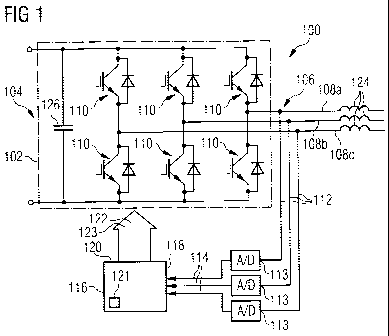
Fig. 1 shows a converter device 100 in accordance with em-
bodiments of the herein disclosed subject matter. In accor-
dance with an embodiment, the converter device 100 comprises
a converter, generally indicated at 102. The converter 102
has an input 104 for receiving an input voltage, e.g. a DC
voltage and an output 106 for providing an output power by
the switching operation of the converter 102. In an embodi-
ment, the output power is a three-phase power. Accordingly,
the output 106 comprises three output lines 108a, 108b, 108c
corresponding to the three phases.
In accordance with an embodiment, the converter comprises a
pulse width modulation bridge having two switching elements
110 per phase. The switching elements 110 are insulated gate
bipolar transistors (IGBTs) having a freewheel diode con-
nected in parallel as shown in Fig. 1.
Further, the converter device 100 has a feedback line 112
coupled to each output line 108a, 108b, 108c to sense the
output current of each phase. Further, an analog/digital con-
verter (A/D converter) 113 is provided for each phase for
providing for each phase a respective feedback signal 114 in
response to the sensed current.
The converter device further comprises a controller 116 con-
figured in accordance with embodiments of the herein dis-
201023835 CA 02767709 2012-02-10
closed subject matter. The controller 116 has an input 118
for receiving the feedback signals 114 which depend on the
output power of the converter 102. Further, the controller
comprises an output 120 for providing a control signal 122 to
5 the converter 102 to thereby control the switching operation
of the converter 102. For example, in an embodiment, the
switching signals 122 are IGBT gate signals provided to the
gates of the IGBTs.
10 In an embodiment, the controller 116 includes a processor de-
vice 121 configured for carrying out a computer program that
provides at least one function of the controller 116.
In accordance with an embodiment, the control signal 102 cor-
responds to a switching pattern that is updated in response
to the feedback signals 114. Further, the control signal 122
includes an harmonic compensation signal 123 which reduces
higher harmonics in the output power, the higher harmonics
originating from a time delay between taking the feedback
signal and the updating of the switching pattern.
Further shown in Fig. 1 are windings 124 of a reac-
tor/inductor and a filtering capacitor 126. However, these
elements perform their usual function and are not further de-
scribed here.
In the following, possible operation schemes of a converter
device are described to further illustrate advantages of as-
pects and embodiments of the herein disclosed subject matter.
Fig. 2 illustrates current sampling over a PWM period wherein
an average of N samples during a previous PWM period is used
as current feedback. Shown in Fig. 2 are the control signal
components 122a, 122b, 122c corresponding to the phases on
lines 108a, 108b, 108c in Fig. 1 over time t. Further shown
in Fig. 2 is the PWM period 128 corresponding to a fixed
switching frequency. The PWM period is defined as PWM period
= 1/(switching frequency).
201023835 CA 02767709 2012-02-10
11
Typically in the current is sampled many times during a com-
plete PWM period 128, the sampling being indicated at 130.
The average of these multiple (e.g. N) samples is used as the
current feedback variable, leading to an updated switching
pattern at a time indicated at 132. While the described
method provides a method good attenuation of the PWM switch-
ing frequency related harmonic currents, it introduces a fi-
nite phase delay due to the time delay between sampling the
current during intervals la and lb, doing the necessary
mathematical calculations during 2a, and respectively chang-
ing the PWM voltage at the output of the bridge. It is desir-
able from the point of view of control system stability, par-
ticularly when arrays of wind turbines, or arrays of network
connected PWM bridges are considered that these phase delays
are minimised. With a scheme such as shown in Fig. 2, the ef-
fective delay is 500 microseconds (ps) (assuming 400 ps PWM
period which is typical e.g. for wind turbines).
Fig. 3 illustrates `synchronous' current sampling at a mid-
point 302 of the zero vector wherein a current sample point
is at a PWM period midpoint. The switching pattern is updated
at the next midpoint of the zero vector, indicated at 304.
The arrows 306 indicate the time delay between taking the
feedback signal and the updating of the switching pattern.
When the IGBT's are switched such that either all the upper
devices are ON, or all the lower devices are ON this is known
as a zero vector and is equivalent to the upper and lower
peaks in a sine triangular comparison method of generating
PWM pulses. As mentioned, the current is sampled at the mid-
point of the zero vector (e.g. in the middle of the PWM pe-
riod) as shown in Fig. 3. The midpoint of zero vector is in-
dicated by the vertical lines in Fig. 3. The currents are
sampled at this point, i.e. at a midpoint of a zero vector,
since favourable cancellation of the switching frequency har-
monics results thereof. Using the technique of synchronously
sampling the three phase current feedbacks and updating the
201023835 CA 02767709 2012-02-10
12
PWM pattern at the midpoint of the zero vectors (asymmetric
PWM), as shown in Fig. 3, results in an effective delay be-
tween the current sample and the voltages appearing on the
output of the bridge of a 3/4 PWM period. Assuming a 400ps
PWM period this equates to 300us delay.
However, the constraint of updating the PWM switching pattern
only at the mid points of the zero vectors introduces a delay
of 1/2 PWM period. Whilst this may suit microprocessor sys-
tems by permitting sufficient time for control calculation to
be performed, it does not offer the optimal behaviour from a
control loop stability point of view, as the delay introduced
is not at its absolute minimum.
Given that the control calculations are performed every 1/2
PWM period, this results in an effective delay of 100ps. In
an ideal consideration where A/D conversion times are zero,
and microprocessor CPU resource is infinite then this 100ps
would be the minimum delay possible.
Experience of wind farm collector systems to date has shown
that due to resonances in the wind farm collector system it
is highly desirable to have the minimum phase lag (phase de-
lay) introduced by the controller. Resonances are usually
caused e.g. by medium voltage (MV) and/or high voltage (HV)
cables, or potentially capacitor banks for VAr compensation,
or AC filters. The minimum phase lag allows to achieve a ro-
bust current control arrangement, both at an individual net-
work bridge (or turbine) level and across the complete array
of network bridges (or turbines). This minimal phase delay
reduces the likelihood of the current controller interacting
with AC system resonances.
However, the methods of current sampling and updating of the
PWM switching pattern as described with regard to Fig. 2 and
Fig. 3 appear suitable for motor drive converter devices.
201023835 CA 02767709 2012-02-10
13
In contrast, the connection of high power, GRID connected
voltage sourced inverters, which is one application of the
herein disclosed subject matter, has different requirements.
The fact that converters in such applications are connected
e.g. within wind farm collector systems which contain reso-
nances place new and demanding requirements on the current
loop stability which are more demanding than standard motor
control applications.
However, updates of the switching pattern within the PWM pe-
riod elsewhere than at the midpoint,of the zero vector is not
a straightforward task because, updating the PWM modulating
waveform (it is a discrete signal) elsewhere within the PWM
period results in an increase in the low order harmonic con-
tent of the PWM voltage.
However, low order harmonics are desirably minimized and
hence updating the switching pattern (or, in embodiments up-
dating the PWM modulating waveform) elsewhere than at the
midpoint of the zero vector appears not suitable without the
concepts provided by aspects and embodiments of the herein
disclosed subject matter.
However it should be noted that traditional 'analog' type PWM
schemes where the sine triangle comparison is made, the sine
or modulating waveform is a continuous (not sampled) wave-
form.
Advantageously, aspects and embodiments of the herein dis-
closes subject matter allow updating the switching pattern at
a point in time other than the subsequent midpoint of the
zero vector.
For example, in order to try and reduce the delay between
sampling the current and updating the voltage of the PWM
bridge a scheme such as presented in Fig 4 is proposed. The
current feedback is still sampled at the midpoint 302 of
201023835 CA 02767709 2012-02-10
14
the zero vector. This has the advantage of minimising the
harmonic content within the sampled current feedback signal.
However in accordance with an embodiment, Fig. 4 shows the
updating of the switching pattern at a point in time 404
other than the subsequent midpoint of the zero vector, a de-
lay (tc) 406 after the current sample is taken. In an embodi-
ment, the delay 406 is the time taken for the microprocessor
to perform the necessary calculations, and these calculations
can now be minimised to reduce the effective delay introduced
by the controller.
For illustration purposes it is assumed that the delay 406 is
tc = 50ps. With the scheme proposed in Fig. 4 the delay in-
troduced by the controller can now be reduced to
1/4 PWM period + 50 ps. Hence, based on a 400 is PWM period
the current is sampled twice per PWM period, i.e. every
200 ps. With the PWM pattern being updated 50ps after the
current sampling, this results in an effective delay of
150 ps. An advantage of thereof is that the point at which
the open loop phase, of the controller response, rolls off to
-180 is now 0.5/150ps = 3333 Hertz (Hz).
Similar considerations for the previous scheme shown in
Fig. 3, which has an effective delay of 300 ps (3/4 PWM pe-
riod), show that a -180 phase is obtained at approximately
0.5/300ps = 1666 Hz.
Further, similar considerations for the previous scheme shown
in Fig. 2, which has an effective delay of 500 ps, show that
the phase rolls off at 0.5/500ps = 1 kHz.
If in a control system the gain of an open loop system is
greater than unity at any frequency above which the
phase rolls off to an angle smaller or equal (<=) -180 then
the corresponding closed loop system is unstable. In reality
AC series resonances result in a gain greater than unity.
201023835 CA 02767709 2012-02-10
So in principle one consequence of the exemplary minimized
delay scheme suggested above is that the closed loop system
is now immune to resonances which are at frequencies smaller
or equal to 3333 Hz, whereas the schemes shown in Fig. 2 and
5 Fig. 3 are only immune to resonances at frequencies smaller
than 1000 Hz in the case of Fig. 2, or smaller than 1666 Hz
in the case of Fig. 3. In practice it is likely that reso-
nances will exist at frequencies smaller than (<) 3kHz such
that these schemes do not offer the possibility of being com-
10 pletely immune to AC system resonances. However, having a
controller which is immune to resonances up to 3333 Hz before
the phase rolls off can be considered a significant improve-
ment.
15 However the consequence of not updating the PWM pattern at
the midpoint of the zero vector is an increase in the low or-
der harmonic voltage content of the PWM output voltage.
Fig. 5 shows the magnitude of the harmonic current (z-axis)
over the harmonic order (x-axis) and the switching pattern
update offset tc (y-axis).
The first harmonic (fundamental component) corresponds to the
desired signal. Higher harmonics (shown up to about 20th or-
der) appear if the switching pattern are updated elsewhere
than at the midpoint of the zero vector. As can be seen from
Fig. 5, at the zero vectors, effectively 0 }.s and 200 ps on
the Y axis, the low order harmonic current is approximately
zero, however at points in between this is not the case be-
sides a minimum at 100 us.
Further, Fig. 5 shows a strong increase in the 5th harmonic
current (but not only the 5th harmonic) for the switching
pattern being updated at points other than the midpoint of
the zero vector. For the purposes of this discussion the
spectra shown in Fig. 5 can be considered a harmonic voltage
spectra.
201023835 CA 02767709 2012-02-10
16
However, the simulation result shown in Fig. 5 was obtained
without a harmonic compensation signal which reduces higher
harmonics in the output power.
In the following, embodiments relating to the harmonic com-
pensations signal are further discussed in the following.
According to an embodiment, the harmonic compensation signal
is obtained by introducing a compensation waveform to the PWM
modulation waveform, the compensation waveform compensating
the harmonic voltages introduced by updating the switching
pattern at points other that the midpoint of the zero vec-
tors.
Fig. 6 illustrates for a single phase the determination of a
PWM switching pattern 602 from an exemplary modulating wave-
form 604 and a triangular carrier 606 (in arbitrary units).
The PWM switching pattern 602 (wherein uc is the voltage over
capacitor 126 in Fig. 1), the modulating waveform 604 and the
triangular carrier 606 are drawn over time t in seconds t(s).
A modulating waveform such as shown for a single phase in
Fig. 6, can be derived by several different means, typically
a third harmonic voltage component, or series of triplen har-
monic voltages is/are added to the fundamental to maximise
the resulting output voltage. Space vector PWM achieves a
similar output voltage harmonic spectrum by mathematical cal-
culation of the IGBT switching times. Points in time where
the modulating waveform 604 crosses the triangular carrier
606 indicate a switching event, as is exemplary illustrated
by the lines 610.
If a series of harmonic components of suitable phase and mag-
nitude are added to the modulating waveform 604 of
Fig. 6, to compensate for the harmonic voltages present in
the PWM voltage spectrum of Fig. 5, then the resulting
201023835 CA 02767709 2012-02-10
17
PWM voltage will contain no low order harmonic voltage compo-
nents or the low order harmonic components are at least re-
duced.
Fig 7 shows a controller 116 in accordance with embodiments
of the herein disclosed subject matter.
In an exemplary embodiment, the controller 116 comprises a
vector control unit 702 and a modulation calculator 704 which
receives a q-axis component (Vq) 706, a d-axis component (Vd)
708 as well as a phase angle 710 indicative of the position
of the rotating reference frame defining the q-axis and the
d-axis of the vector control. In response to the values re-
ceived from the vector control unit 702, the modulation cal-
culator 704 calculates a modulation depth 712 and a modula-
tion angle 714. Further, a modulation signal generator 716 is
provided, the modulation signal generator 716 being config-
ured for providing a modulation signal, e.g. in the form of a
modulating waveform 604.
Further, in accordance with an embodiment, a compensation
generator 718 is provided, the compensation generator 718 be-
ing configured for generating a harmonic compensation compo-
nent 720 in response to input parameters. In an embodiment,
the input parameters are the modulation depth 712, the modu-
lation angle 714 and the time delay tc between the sampling
of the current and the corresponding switching pattern up-
date. In an embodiment, the harmonic compensation component
720 is a function of these variables, modulation depth 712,
the modulation angle 714 and the time delay to 406. However,
in accordance with embodiments, such a function may be de-
fined in the compensation generator 718 by a lookup table.
Further, in accordance with an embodiment, the controller 116
is configured for providing the control signal 122 depending
on the modulation signal 604 and the harmonic compensation
component 720.
201023835 CA 02767709 2012-02-10
18
In an embodiment, the modulation signal generator 716 uses a
triplen enhanced sinewave reference waveform, or Look up ta-
ble, or does an on line calculation to obtain the amplitude,
i.e. the modulating waveform 604. In accordance with an em-
bodiment, the additional harmonic compensation component 720
is added to the modulating waveform 604 by an adder 724, to
thereby generate a summing signal 726.
In accordance with an embodiment, the controller further com-
prises a signal processing unit 728 for processing the sum-
ming signal 726, thereby generating the control signal 122.
For example, in an embodiment the modulating waveform 604 is
compared to the triangular carrier waveform 722 by the signal
processing unit 728 to produce the individual control signals
122 which compensate for the phase lag, i.e. the harmonics
that originate from a time delay between taking the feedback
signal and the updating of the switching pattern.
Deadtime compensation and or other bridge linearization fea-
tures are not shown in this figure, and are not specifically
compensated for with this technique. It is believed that al-
ternative techniques exist to achieve this.
According to an embodiment, the harmonic compensation compo-
nent 720 contains a series of normalized harmonic voltages
as a function of modulation depth, angle and 'tc' the time
delay between current sampling and switching pattern update.
According to an embodiment, a lookup table is provided in or-
der to provide the harmonic compensation component 720 as a
function of one or more defining parameters such as a modula-
tion depth, a modulation angle and the time delay. In accor-
dance with an embodiment, the lookup table has stored therein
a plurality of compensation indicators, each compensation in-
dicator corresponding to a respective harmonic compensation
component. The compensation generator is configured for gen-
erating the harmonic compensation component on the basis of a
selected compensation indicator. Typically the lookup table
201023835 CA 02767709 2012-02-10
19
(compensation table) are calculated offline based on a de-
sired 'tc' 406 such that the resulting PWM voltage contains
none of the harmonic voltages of Fig. 5 across the entire op-
erating range of modulation depth.
The described technique permits a significant and technically
advantageous reduction in the phase shift introduced by the
digital current controller across a frequency range that is
related to wind farm AC collector systems, and should
not suffer from undesirable low order harmonic voltages in
the output PWM waveform.
According to embodiments of the invention, any suitable en-
tity (e.g. controllers, components, units and devices) dis-
closed herein are at least in part provided in the form of
respective computer programs which enable a processor device
to provide the functionality of the respective entities as
disclosed herein. According to other embodiments, any suit-
able entity disclosed herein may be provided in hardware. Ac-
cording to other - hybrid - embodiments, some entities may be
provided in software while other entities are provided in
hardware.
It should be noted that any entity disclosed herein (e.g.
controllers, components, units and devices) are not limited
to a dedicated entity as described in some embodiments.
Rather, the herein disclosed subject matter may be imple-
mented in various ways and with various granularity on device
level or software module level while still providing the de-
sired functionality. Further, it should be noted that accord-
ing to embodiments a separate entity (e.g. a software module,
a hardware module or a hybrid module) may be provided for
each of the functions disclosed herein. According to other
embodiments, an entity (e.g. a software module, a hardware
module or a hybrid module (combined software/hardware mod-
ule)) is configured for providing two or more functions as
disclosed herein. According to an embodiment, the controller
comprises a processor device including at least two proces-
201023835 CA 02767709 2012-02-10
sors for carrying out at least one computer program corre-
sponding to a respective software module.
It should be noted that the term "comprising" does not ex-
5 clude other elements or steps and the "a" or "an" does not
exclude a plurality. Also elements described in association
with different embodiments may be combined. It should also be
noted that reference signs in the claims should not be con-
strued as limiting the scope of the claims.
In order to recapitulate the above described embodiments of
the present invention one can state:
There is provided a controller for a converter and a respec-
tive method of operating such a controller. The converter re-
ceives an input power and provides an output power by a
switching operation wherein in an embodiment the output power
has at least two phases. In accordance with embodiments, the
controller comprises an input for receiving a feedback signal
depending on the output power of the converter; and an output
for providing a control signal to the converter to thereby
control the switching operation of the converter, the control
signal corresponding to a switching pattern that is updated
in response to the feedback signal; the control signal in-
cluding an harmonic compensation signal which reduces higher
harmonics in the output power, the higher harmonics originat-
ing from a time delay between taking the feedback signal and
the updating of the switching pattern.
Embodiments of the herein disclosed subject matter include
one or more of the following advantages, as is readily recog-
nized by a skilled person:
1. A significant and advantageous reduction in the phase
shift/time delay introduced by the current controller can be
achieved, with respect to current loop stability and the
overall wind farm current loop stability. The ability to sig-
nificantly increase the effective phase margin means that a
201023835 CA 02767709 2012-02-10
21
robust current controller can be implemented which is at
least to some extent immune to the electrical system to which
the current controller is connected. The ability to do this
means that a 'one size fits all' approach can be taken to a
turbines electrical connection as it will be less likely, or
not required, that individual studies are required to assess
the stability margin of a particular wind farm arrangement.
Typically from one windfarm to the next the collector system
will have a range of resonance frequencies
associated with it as will have medium voltage and/or high
voltage cables or overhead lines (and/or locally connected
power factor correction equipment or tuned filters).
2. The ability to achieve the aforementioned point 1, and not
compromise the harmonic emissions of the turbine due to har-
monic voltages in the resulting PWM is achieved by the addi-
tion of the harmonic compensation table within the PWM
modulating waveform generator.
3. Embodiments allow updating the PWM modulation waveform at
a point other than the midpoint of the zero vectors.
4. An advantage of embodiments of the herein discloses sub-
ject matter is that power filters may need not be fitted to
stabilize particular wind farm collector systems as the im-
provements in control result in sufficient phase margin,
rather than needing to resort to a power hardware solution,
which would involve significant cost.