Note: Descriptions are shown in the official language in which they were submitted.
CA 02768436 2016-12-16
247777
METHOD AND SYSTEM OF A SENSOR INTERFACE HAVING DYNAMIC
AUTOMATIC GAIN CONTROL DEPENDENT ON SPEED
CROSS REFERENCE TO RELATED APPLICATION
This application is related to CA Patent Application 2,768,566, filed on
February 16, 2012.
FIELD OF THE INVENTION
Embodiments of the invention described relate to a magnetic sensor interface.
BACKGROUND OF THE INVENTION
In many instances, machines such as for example electric motors, electric
generators,
internal-combustion engines, jet engines, turbines, and the like, and the
systems they
drive, are actively monitored by various monitoring systems for performance
and
operational characteristics including for example vibration, heat, noise,
speed, electrical
characteristics (e.g., current, voltage, resistance, etc.), environmental
effects, and the like.
Generally, the monitoring systems that monitor these machines are comprised of
one or
more sensors or transducers that are proximate to and associated with the
machine. For
example, passive magnetic or reluctance sensors may be used by monitoring
systems.
Hereinafter, these sensors will be referred to simply as "sensors, "magnetic
sensors," or
"passive magnetic sensors," which is intended to include passive magnetic and
reluctance
sensors.
Generally, passive magnetic sensors are constructed of a permanent magnet and
a coil
with signal wires connecting to each side of the coil. The magnet creates a
field (lines of
flux), which extends from the end of the magnetic sensor into the air. As a
ferrous object
approaches the tip of the magnetic sensor (i.e., the probe tip), the object
interacts with the
magnetic field originating from the magnet encased in the magnetic sensor,
thereby
inducing a current flow in the coil and in turn creating alternating current
(AC) voltage
1
CA 02768436 2012-02-16
247777
that can be seen on the signal wires acting as the magnetic sensor outputs. As
the target
enters and then leaves area occupied by the flux lines, this creates a
positive voltage peak
followed by a negative voltage peak. The voltage output can appear to be
sinusoidal in
nature, but can be distorted depending on the material composition and
geometry of the
target. Several factors contribute to the characteristics of the output signal
generated by
passive magnetic sensors including surface speed of the target, gap size,
target geometry,
and load impedance.
Surface speed is the speed at which the target passes the magnetic sensor's
probe tip and
directly affects the amplitude of the pulse created by the magnetic sensor.
The exact
function relating target speed to output voltage varies from magnetic sensor
to magnetic
sensor, but correlation between speed and output voltage is nearly a linear
function
(proportional). Gap size refers to the distance between the target and the
magnetic
sensor's probe tip when the target passes and it influences the output voltage
as well. The
smaller the gap, the larger the output voltage will be. Typical gap settings
for magnetic
sensors can be around 25 to 30 mils. Generally, the relationship between gap
size and
voltage output is nonlinear in nature. Decreasing the gap can drastically
increase output
voltage. The geometric dimensions of a target can also affect the amplitude
and shape of
the output voltage. Generally, the larger the target, the greater the
amplitude. Load
impedance, relative to the internal impedance of the magnetic sensor, dictates
the amount
of magnetic sensor output voltage that will be seen by that load. Magnetic
sensors are
generally designed with the lowest practical impedance consistent with
providing
maximum output. The load impedance should be high in relation to the impedance
of the
magnetic sensor to minimize the voltage drop across the coil and to deliver
the maximum
output to the load. Generally the load impedance should be at least 10 times
that of the
internal impedance of the magnetic sensor.
Benefits of using magnetic sensors include that they are passive and therefore
don't
require external power, they are simplistic in design and therefore highly
reliable, and
they are generally low cost. However, there are challenges to using these
sensors as well.
2
CA 02768436 2012-02-16
247777
One challenge is that output signal amplitude can fluctuate drastically based
on speed.
This can make it difficult to analyze startup data characteristics of a
machine ramping
from, for example, zero to 3600 rpm. For example, magnetic sensor output
voltage
changes drastically (e.g., 10mVp-p to 200Vp-p) with respect to the speed of
the passing
target. This characteristic can pose a challenge when monitoring the magnetic
sensor
output of a target passing at a low speed with the same accuracy of the output
when the
target passes at high speed. Slow speed signals need gain to improve the
signal to noise
ratio while high speed signals need to be attenuated to avoid clipping or
distortion due to
circuit limits. Another challenge is that due to the passive nature of
magnetic sensors, a
magnetic pickup has less drive strength and will not be able to drive a signal
through long
cables. Furthermore, magnetic sensors cannot be used for an accurate gap
reading. While
the amplitude can be indicative of the gap, the gap size cannot be accurately
determined
with a given output voltage due to the various other factors that influence
the output as
discussed above.
Therefore, systems and methods that overcome challenges in the art, some of
which are
described above, are desired. In particular, providing dynamic automatic gain
control
using a speed input for a magnetic sensor that can be used to improve the
accuracy of an
output of the magnetic sensor for a target passing at a low speed and of the
same target
when the target passes at high speed would be valuable in addressing the above-
described
challenges.
BRIEF DESCRIPTION OF THE INVENTION
Embodiments of the invention described herein provide a magnetic sensor
interface
capable of adjusting signal conditioning dynamically using a speed signal that
measures
the current speed of the target such that the true positive and negative peaks
of the input
signal are maintained for the given target across its entire speed range (0-
Max rpm),
therefore increasing the signal to noise ratio at low speeds and avoiding
clipping or
distortion at high speeds.
3
CA 02768436 2012-02-16
247777
In one aspect, a method is described. The method comprises receiving an
alternating
differential voltage signal from a sensor. The differential voltage signal has
an amplitude
that changes relative to a change in speed of a target. The alternating
differential voltage
signal is converted to an attenuated single-ended voltage signal that can be
dynamically
scaled. The attenuated single-ended voltage signal can be scaled by
multiplying the
attenuated single-ended voltage signal by a scaling factor. The scaling factor
is selected
relative to the speed signal and is selected relative to a signal-to-noise
ratio of the scaled
attenuated single-ended voltage signal.
In another aspect, a system is described. The system is comprised of a sensor
configured
to produce an alternating differential voltage signal that has an amplitude
that changes
relative to a change in speed of a target. Further comprising the system is a
first circuit
that receives the alternating differential voltage signal and converts the
alternating
differential voltage signal to an attenuated single-ended voltage signal. A
speed sensor or
transducer produces a speed signal that indicates the current speed of the
target. A
second circuit dynamically scales the attenuated single-ended voltage signal
by
multiplying the attenuated single-ended voltage signal by a scaling factor.
The scaling
factor is selected relative to the speed signal and is selected relative to a
signal-to-noise
ratio of the scaled attenuated single-ended voltage signal.
Additional advantages will be set forth in part in the description which
follows or may be
learned by practice. The advantages will be realized and attained by means of
the
elements and combinations particularly pointed out in the appended claims. It
is to be
understood that both the foregoing general description and the following
detailed
description are exemplary and explanatory only and are not restrictive, as
claimed.
BRIEF DESCRIPTION OF THE DRAWINGS
The accompanying drawings, which are incorporated in and constitute a part of
this
specification, illustrate embodiments and together with the description, serve
to explain
the principles of the methods and systems:
4
CA 02768436 2012-02-16
247777
FIG. 1 is block diagram of one embodiment of a system according to the present
invention;
FIG. 2 is a schematic diagram of an embodiment of a circuit that can be used
to convert
the alternating differential voltage signal to an attenuated single-ended
voltage signal
according to one aspect of the present invention;
FIG. 3 is a schematic diagram of an embodiment of a circuit that can be used
to
dynamically scale the attenuated single-ended voltage signal according to one
aspect of
the present invention;
FIG. 4 is a flowchart that illustrates operations that may be taken in order
to provide
dynamic automatic gain control using a speed signal for a magnetic sensor; and
FIG. 5 is a block diagram illustrating an exemplary operating environment for
performing
the disclosed methods.
DETAILED DESCRIPTION OF THE INVENTION
Before the present methods and systems are disclosed and described, it is to
be
understood that the methods and systems are not limited to specific synthetic
methods,
specific components, or to particular compositions. It is also to be
understood that the
terminology used herein is for the purpose of describing particular
embodiments only and
is not intended to be limiting.
As used in the specification and the appended claims, the singular forms "a,"
"an" and
"the" include plural referents unless the context clearly dictates otherwise.
Ranges may
be expressed herein as from "about" one particular value, and/or to "about"
another
particular value. When such a range is expressed, another embodiment includes
from the
one particular value and/or to the other particular value. Similarly, when
values are
expressed as approximations, by use of the antecedent "about," it will be
understood that
the particular value forms another embodiment. It will be further understood
that the
endpoints of each of the ranges are significant both in relation to the other
endpoint, and
CA 02768436 2012-02-16
247777
=
independently of the other endpoint. Further, when examples of ranges are
provided
herein, it is to be appreciated that the given ranges also include all
subranges
therebetween, unless specifically stated otherwise.
"Optional" or "optionally" means that the subsequently described event or
circumstance
may or may not occur, and that the description includes instances where said
event or
circumstance occurs and instances where it does not.
Throughout the description and claims of this specification, the word
"comprise" and
variations of the word, such as "comprising" and "comprises," means "including
but not
limited to," and is not intended to exclude, for example, other additives,
components,
integers or steps. "Exemplary" means "an example of" and is not intended to
convey an
indication of a preferred or ideal embodiment. "Such as" is not used in a
restrictive
sense, but for explanatory purposes.
Disclosed are components that can be used to perform the disclosed methods and
systems. These and other components are disclosed herein, and it is understood
that when
combinations, subsets, interactions, groups, etc. of these components are
disclosed that
while specific reference of each various individual and collective
combinations and
permutation of these may not be explicitly disclosed, each is specifically
contemplated
and described herein, for all methods and systems. This applies to all aspects
of this
application including, but not limited to, steps in disclosed methods. Thus,
if there are a
variety of additional steps that can be performed it is understood that each
of these
additional steps can be performed with any specific embodiment or combination
of
embodiments of the disclosed methods.
The present methods and systems may be understood more readily by reference to
the
following detailed description of preferred embodiments and the Examples
included
therein and to the Figures and their previous and following description.
As described herein, embodiments of the invention provide a reluctance or
magnetic
sensor interface circuit capable of adjusting signal conditioning dynamically
and relative
6
CA 02768436 2012-02-16
247777
=
to a speed signal from a target such that the true positive and negative peaks
of the input
signal from the reluctance or magnetic sensor are maintained for a given
target across its
entire speed range (0-Max rpm). Magnetic sensor output voltages can change
drastically
(e.g., 10mVp-p to 200Vp-p) with respect to the speed of a passing target. This
characteristic poses a challenge when monitoring the sensor output of a target
passing at a
low speed with the same accuracy of the output when the target passes at high
speed.
Slow speed signals need gain to improve the signal to noise ratio while high-
speed
signals may require attenuation to avoid clipping or distortion due to circuit
limits.
Therefore, the technical effect of embodiments described herein is to provide
a way to
monitor the performance/behavior of a given target across its entire speed
range (0-Max
rpm) with a magnetic sensor utilizing a speed signal from the target.
Embodiments of
this invention allow the capture of signal content from low amplitude signals
that
previously would have been difficult to separate from noise. Embodiments also
provide
an opportunity for better signal to noise ratio across a wide range of target
speeds and
their corresponding signal amplitudes because of the dynamic scaling and use
of the
speed signal.
Systems and methods described herein provide a magnetic sensor interface
circuit
capable of adjusting signal conditioning dynamically using a speed signal from
a target
such that the true positive and negative peaks of the input signal are
maintained. In one
aspect, an embodiment of the interface circuit accepts a differential voltage
from a
magnetic sensor, which is converted to a single ended voltage and attenuated
(if
necessary) to avoid signal clipping. The attenuated single-ended voltage
signal is scaled
(gained or attenuated) relative to its signal to noise ratio without clipping
or altering the
signal waveform. In one aspect, the attenuated single-ended voltage signal is
scaled to
improve or maximize the signal to noise ratio. In one aspect, the gain or
attenuation is
selected by an algorithm executed by a digital processor or field programmable
gate array
(FPGA) that considers at least two inputs. The first input communicates the
speed of the
magnetic sensor's target. The second input is a digital representation of the
analog voltage
seen across the magnetic sensor contacts, which comes from an Analog-to-
Digital
7
CA 02768436 2012-02-16
247777
=
Converter (ADC). The ADC receives its input from the scaled attenuated single-
ended
voltage described herein. This provides a feedback loop that allows
embodiments of the
invention to detect the onset of clipping or signal alteration and adjust the
scaling to
ensure this does not happen. Embodiments also provide a mechanism to control
the signal
conditioning and scaling based on an external speed input.
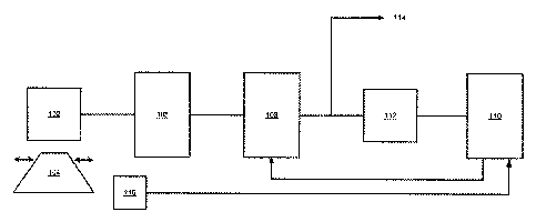
FIG. 1 illustrates an overview block diagram of one embodiment of the present
invention.
The sensor 102 detects a target 104 passing proximate to the sensor 102. As
described
herein, in one aspect the sensor 102 can be a passive magnetic or reluctance
sensor.
Generally, the target 104 passes by the sensor 102, thus producing a voltage
pulse or
signal by the sensor 102. However, in another aspect, the sensor 102 moves
past the
target 104 and produces the voltage signal. The voltage signal produced by the
sensor
102 is related to several factors including target 104 material, target 104
geometry or
shape, gap size between the target 104 and sensor 102, and the speed at which
the target
104 passes the sensor 102 (or the sensor 102 passes the target 104). In one
aspect, the
voltage signal is an alternating differential voltage pulse (i.e., not
referenced to ground or
any other common point). In one aspect, the voltage signal can be symmetrical
or
asymmetrical about a horizontal (zero) axis. The amplitude of the alternating
voltage
signal changes over time as the target 104 approaches, moves beneath and
passes by the
sensor 102 (or the sensor 102 approaches and moves past the target 104). In
one aspect,
the amplitude of the alternating voltage signals changes relative to change in
speed of the
target 104. In one aspect, the alternating voltage signal is a sine wave. In
one aspect, the
alternating voltage signal is not a sign wave. In one aspect, the sensor 102
is a passive
magnetic sensor as available from one of many different manufacturers. In one
aspect,
the sensor 102 can be a passive magnetic sensor or variable reluctance sensor
as available
from Al-Tek Instruments, Inc. (Cheshire, CT). In one aspect, the sensor 102
can be an
Al-Tel model number 70085-1010 passive magnetic sensor. The target 104 can be
various devices. In one aspect, the target 104 can be the blade of a turbine,
such as a
steam turbine, gas turbine, or the like. In one aspect, the target 104 can be
the blade of a
8
CA 02768436 2012-02-16
247777
compressor, such as a compressor used in a gas turbine or the like. In one
aspect, the
target 104 can be a gear tooth.
In one aspect, the alternating differential voltage signal produced by the
sensor 102 is
received by a circuit 106. In one aspect, the circuit 106 receives the
alternating
differential voltage signal and converts the alternating differential voltage
signal to an
attenuated single-ended voltage signal (i.e., referenced to ground or another
common
point). In one aspect, the circuit 106 attenuates or gains the alternating
differential
voltage signal depending upon the peak-to-peak value of the alternating
differential
voltage signal. In one aspect, the circuit 106 attenuates the alternating
differential voltage
by a fixed amount (i.e., the peak-to-peak value of the alternating
differential voltage is
constantly decreased by 10 percent, by 15 percent, by 20 percent, etc.). In
one aspect, the
circuit 106 converts the alternating differential voltage signal to the
attenuated single-
ended voltage signal by attenuating the alternating differential voltage
signal by a fixed
amount such that the attenuated single-ended voltage signal is less than or
equal to a
maximum attenuated voltage. In one aspect, the circuit 106 converts the
alternating
differential voltage signal to an attenuated single-ended voltage signal by
multiplying the
alternating differential voltage signal by a ratio of the maximum attenuated
voltage to the
maximum peak-to-peak value of the alternating differential voltage signal. In
one aspect,
the maximum peak-to-peak value of the alternating differential voltage signal
can be
about 250 volts peak-to-peak and the maximum attenuated voltage of the
attenuated
single-ended voltage signal can be about 30 volts peak-to-peak. In one aspect,
the circuit
106 comprises a resistor divider 202 and an operational amplifier having a
single-ended
output 204 as shown in FIG. 2. FIG. 2 is a schematic diagram of an embodiment
of a
circuit 106 that can be used to convert the alternating differential voltage
signal to an
attenuated single-ended voltage signal according to one aspect of the present
invention.
In one aspect, converting the alternating differential voltage signal to an
attenuated
single-ended voltage signal comprises using the resistor divider 202 to divide
the
alternating differential voltage signal and providing a differential input to
the operational
amplifier having a single-ended output 204. In one non-limiting example,
resistor divider
9
CA 02768436 2012-02-16
247777
202 can be comprised of resistors having the following values: R142 = 4.99
kilo-ohms,
R143 = 4.99 kilo-ohms, R144 = 3.01 kilo-ohms, R145 = 121 kilo-ohms and R146 =
121
kilo-ohms. Also, in one non-limiting example, the operational amplifier
circuit having a
single-ended output 204 can be comprised of resistors and capacitors having
the
following values: R147 = 49.9 kilo-ohms, R148 = 49.9 kilo-ohms, R284 = 2.0
kilo-
ohms, C103 = 5.6 Pico-farads, and C104 = 5.6 Pico-farads. The circuit of FIG.
2 is
provided as a non-limiting example and it is to be appreciated that other
circuits can be
used to perform the same function.
Further comprising the system of FIG. 1 is a speed sensor 116 that senses the
current
speed at which the target 104 is moving and produces a speed signal relative
to the speed
of the target 104. Conversely, the speed sensor 116 can sense the speed at
which the
magnetic sensor 102 moves past the target 104 (if the target 104 were
stationary and the
magnetic sensor 102 were moving). In one aspect, the speed signal from the
speed sensor
116 is provided to a field programmable gate array (FPGA) or digital processor
110,
which uses the speed signal to scale the attenuated single-ended voltage
signal according
to the algorithm described herein. In various aspects, the speed sensor 116
can be, for
example, an eddy current probe (i.e., a proximity sensor), a magnetic pick-up
sensor, an
optical speed sensor, a capacitive sensor, and the like. Though referred to as
a speed
sensor 116, it is to be appreciated that this reference includes a speed
transducer.
As shown in FIG. 1, the attenuated single-ended voltage signal is dynamically
scaled by
multiplying the attenuated single-ended voltage signal by a scaling factor. In
one aspect,
the scaling factor is selected relative to the speed signal and is selected
relative to a
signal-to-noise ratio of the scaled attenuated single-ended voltage signal. In
one aspect,
the scaling factor is selected to improve or maximize the signal-to-noise
ratio of the
scaled attenuated single-ended voltage signal. In one aspect the circuit 106
provides the
attenuated single-ended voltage signal to a second circuit 108. The second
circuit 108
dynamically scales the attenuated single-ended voltage signal. In one aspect,
a field
programmable gate array (FPGA) or digital processor 110 associated with the
second
CA 02768436 2012-02-16
247777
circuit 108 automatically sets the scaling factor such that a product of the
scaling factor
times the attenuated single-ended voltage signal is less than or equal to a
maximum input
signal voltage. In one aspect, the maximum input signal voltage is about 6.5
volts peak-
to-peak. In one aspect, the FPGA or digital processor 110 associated with the
second
circuit 108 automatically sets the scaling factor in accordance with an
algorithm. In one
aspect, the algorithm comprises the FPGA or digital processor 110 receiving a
digital
input representative of the alternating differential voltage signal produced
by the sensor
102 and a speed input representative of the current speed of the target 104
(or of the
magnetic sensor 102 if the target 104 is stationary) and scaling the
attenuated single-
ended voltage signal in proportion to the inputs. In one aspect, the digital
input
comprises the scaled output of the second circuit 108 converted to a digital
signal by an
analog-to-digital convertor (ADC) 112. In one aspect, if the digital input to
the FPGA or
digital processor 110 is below a lower defined value, ValueL, then the scaling
factor is
greater than one and the attenuated single-ended voltage signal is amplified
in order to
increase its signal to noise ratio. In one aspect, if the digital input to the
FPGA or digital
processor 110 is equal to or between a lower defined value, ValueL, and an
upper defined
value, Valueu, then the scaling factor is one and the attenuated single-ended
voltage
signal is neither amplified nor attenuated. In one aspect, if the digital
input to the FPGA
or digital processor 110 is greater than an upper defined value, Valueu, then
the scaling
factor is less than one and the attenuated single-ended voltage signal is
further attenuated
in order to avoid clipping or distortion of the signal. In one aspect, the
scaling factor
determined by the algorithm is adjusted by the speed signal from the speed
sensor 116.
In one aspect, the processor or FPGA 110 can sense the speed of the target 104
and adjust
or scale the attenuated single-ended voltage signal level based on speed to
make sure
clipping or distortion does not occur. In one aspect, the scaling factor as
determined by
the algorithm is multiplied by a ratio of the current speed of the target 104
(or sensor 102)
to the maximum speed of the target 104 (or sensor 102).
In one aspect, an output 114 of circuit 108 can be provided to a monitoring
system such
as a turbine, compressor, or the like blade monitoring system. In one aspect,
the output
11
CA 02768436 2012-02-16
247777
114 has a value that is the same or less than the maximum input voltage level.
In one
aspect, operational characteristics and specifications of the monitoring
system can
determine the value for the maximum input voltage signal. In one aspect,
operational
characteristics and specifications of the ADC 112 can determine the value for
the
maximum input voltage signal.
Referring now to FIGS. 1 and 3, in one aspect, the second circuit 108
dynamically scaling
the attenuated single-ended voltage signal comprises the second circuit 108
dynamically
scaling the attenuated single-ended voltage signal using a scaling op-amp
circuit 304 that
has a digital potentiometer 302 controlled by the FPGA or digital processor
110. The
FPGA or digital processor 110 provides an input to the digital potentiometer
302 that
dynamically scales the attenuated single-ended voltage signal in accordance
with the
above-described algorithm. In one aspect, the FPGA or digital processor 110
scales the
attenuated single-ended voltage signal by receiving a digital representation
of the
attenuated single-ended voltage signal from the ADC 112 and a speed signal
from a
speed sensor 116 and automatically adjusting the digital potentiometer 302
such that the
scaling factor times the attenuated single-ended voltage level is less than or
equal to the
maximum input signal voltage. In one aspect, the scaling factor is 1 or
greater such as,
for example, 1Ø 1.1. 1.2. 2.0, 2.5, 10.0 etc. In another aspect the scaling
factor is less
than 1 such as for example, 0.95, 0.90, 0.5. 0.33, 0.10. 0.01, etc.
FIG. 3 is a schematic diagram of an embodiment of a circuit 108 that can be
used to
dynamically scale the attenuated single-ended voltage signal according to one
aspect of
the present invention. In one aspect, dynamically scaling the attenuated
single-ended
voltage signal comprises the FPGA or processor 110 automatically adjusting the
digital
potentiometer 302 in accordance with the above-described algorithm such that
an output
of a scaling operational amplifier circuit 304 has an improved signal to noise
ratio and is
not so large as to result in clipping or distortion of the signal. In one
aspect, the signal to
noise ratio of the output is maximized. As noted above, the algorithm
considers the speed
of the target 104 (or sensor 102) when scaling the attenuated single-ended
voltage signal.
12
CA 02768436 2012-02-16
247777
In one aspect, an output of the digital potentiometer 302 is used as an input
to the scaling
operational amplifier circuit 304 to provide dynamic scaling of the output of
the scaling
operational amplifier circuit 304. In one non-limiting example, digital
potentiometer 302
can be further comprised of capacitor C124 having a value of 1 micro-farad.
Also, in one
non-limiting example the scaling operational amplifier circuit 304 can be
comprised of
resistors and capacitors having the following values: R173 = 49.9 kilo-ohms,
R174 =
20.0 kilo-ohms, R175 = 10.0 kilo-ohms, R165 = 4.99 kilo-ohms, and C121 = 5.6
Pico-
farads. In one aspect, the digital potentiometer 302 can be a single-channel,
1024-
position digital potentiometer as available from, for example, Analog Devices,
Inc.
(Norwood, MA). In one aspect, the digital potentiometer 302 can be an Analog
Devices,
Inc. model AD5293 digital potentiometer. While the circuit of FIG. 3 is
provided as a
non-limiting example, it is to be appreciated that other circuits can be used
to perform the
same function.
Referring now to FIG. 4, the operations are illustrated that may be taken in
order to
provide dynamic automatic gain control using a speed signal for a magnetic
sensor. At
step 402, an alternating differential voltage signal is received from a
sensor. In one
aspect, the sensor is a passive magnetic sensor. In one aspect, the sensor is
a variable
reluctance sensor. The alternating differential voltage signal has an
amplitude that
changes relative to a change in speed of a target. For example, if the sensor
were
monitoring a stage of blades of a turbine, then the amplitude of the
alternating differential
voltage signal from the sensor would increase as the machine ramps up from
zero
revolutions per minute (rpm) to operating speed (e.g., 3600 rpm). This is
because the
alternating differential voltage signal produced by the sensor is related to a
target's
material composition, a gap between the sensor and the target, and a speed at
which the
target passes the sensor (or sensor passes the target). In one aspect, the
target is a turbine
blade. At step 404, the alternating differential voltage signal is converted
to an
attenuated single-ended voltage signal. In one aspect, the alternating
differential voltage
signal has a maximum peak-to-peak value and converting the alternating
differential
voltage signal to an attenuated single-ended voltage signal comprises the
alternating
13
CA 02768436 2012-02-16
247777
differential voltage signal multiplied by a ratio of a maximum attenuated
voltage to the
maximum peak-to-peak value. In one aspect, the maximum peak-to-peak value of
the
alternating differential voltage signal can be 250 volts peak-to-peak and the
maximum
attenuated voltage of the attenuated single-ended voltage signal can be 30
volts peak-to-
peak. In one aspect, converting the alternating differential voltage signal to
the
attenuated single-ended voltage signal comprises attenuation of the
alternating
differential voltage signal by a fixed amount such that the attenuated single-
ended voltage
signal is less than or equal to the maximum attenuated voltage. In one aspect,
converting
the alternating differential voltage signal to an attenuated single-ended
voltage signal
comprises using a resistor divider to divide the alternating differential
voltage signal and
providing a differential input to an operational amplifier having a single-
ended output.
At step 406, a speed signal is received from a speed sensor. In one aspect,
the speed
signal indicates the current speed of the target relative to the magnetic
sensor. In one
aspect, the speed signal indicates the current speed of the magnetic sensor
relative to the
target. At step 408, a scaling factor is determined. In one aspect, the
scaling factor is
determined from the speed input and a digital representation of the attenuated
singled the
single-ended voltage signal. In one aspect, the scaling factor is selected
relative to the
speed signal and is selected to maximize a signal-to-noise ratio of the scaled
attenuated
single-ended voltage signal. At step 410, the attenuated single-ended voltage
signal is
dynamically scaled by multiplying the attenuated single-ended voltage signal
by the
scaling factor. In one aspect, dynamically scaling the attenuated single-ended
voltage
signal by multiplying the attenuated single-ended voltage signal by a scaling
factor
comprises selecting the scaling factor such that a product of the scaling
factor times the
attenuated single-ended voltage signal is less than or equal to a maximum
input signal
voltage, as described herein. In one aspect, selecting the scaling factor
relative to the
speed signal comprises said scaling factor selected relative to a ratio of the
current speed
of the target to a maximum speed of the target. In one aspect, the maximum
input signal
voltage is 6.5 volts peak-to-peak. In one aspect, dynamically scaling the
attenuated
single-ended voltage signal by multiplying the attenuated single-ended voltage
level by
the scaling factor comprises dynamically scaling the attenuated single-ended
voltage
14
CA 02768436 2012-02-16
247777
signal using a scaling op-amp circuit that has a digital potentiometer
controlled by an
field programmable gate array (FPGA) or digital processor. In one aspect, the
FPGA or
digital processor dynamically scales the attenuated single-ended voltage
signal by
receiving a digital representation of the attenuated single-ended voltage
signal and a
speed signal and adjusting the digital potentiometer such that the scaling
factor times the
attenuated single-ended voltage level is less than or equal to the maximum
input signal
voltage. In one aspect, the scaling factor is 1 or greater such as, for
example, 1Ø 1.1.
1.2. 2.0, 2.5, 10.0 etc. In another aspect the scaling factor is less than 1
such as for
example, 0.95, 0.90, 0.5. 0.33, 0.10. 0.01, etc.
The above system has been described as comprised of units (e.g., the FPGA or
digital
processor 110, etc.). One skilled in the art will appreciate that this is a
functional
description and that software, hardware, or a combination of software and
hardware can
perform the respective functions. A unit, such as the FPGA or processor 110
can be
software, hardware, or a combination of software and hardware. The units can
comprise
the digital potentiometer control software 506 as illustrated in FIG. 5 and
described
below. In one exemplary aspect, the units can comprise a computer 501 as
illustrated in
FIG. 5 and described below. In one aspect, the processor 503 of the computer
501 can be
used to execute the algorithm described above as embodied in computer-
executable code
and to control the digital potentiometer 302 as described herein.
FIG. 5 is a block diagram illustrating an exemplary operating environment for
performing
the disclosed methods. This exemplary operating environment is only an example
of an
operating environment and is not intended to suggest any limitation as to the
scope of use
or functionality of operating environment architecture. Neither should the
operating
environment be interpreted as having any dependency or requirement relating to
any one
or combination of components illustrated in the exemplary operating
environment.
The present methods and systems can be operational with numerous other general
purpose or special purpose computing system environments or configurations.
Examples
of well known computing systems, environments, and/or configurations that can
be
CA 02768436 2012-02-16
247777
suitable for use with the systems and methods comprise, but are not limited
to, embedded
processing units, personal computers, server computers, laptop devices, and
multiprocessor systems. Additional examples comprise machine monitoring
systems,
programmable consumer electronics, network PCs, minicomputers, mainframe
computers, smart meters, smart-grid components, distributed computing
environments
that comprise any of the above systems or devices, FPGA's, and the like.
The processing of the disclosed methods and systems can be performed by
software
components. The disclosed systems and methods can be described in the general
context
of computer-executable instructions, such as program modules, being executed
by one or
more computers or other devices. Generally, program modules comprise computer
code,
routines, programs, objects, components, data structures, etc. that perform
particular tasks
or implement particular abstract data types. The disclosed methods can also be
practiced
in grid-based and distributed computing environments where tasks are performed
by
remote processing devices that are linked through a communications network. In
a
distributed computing environment, program modules can be located in both
local and
remote computer storage media including memory storage devices.
Further, one skilled in the art will appreciate that the systems and methods
disclosed
herein can be implemented via a general-purpose computing device in the form
of a
computer 501. The components of the computer 501 can comprise, but are not
limited to,
one or more processors or processing units 503, a system memory 512, and a
system bus
513 that couples various system components including the processor 503 to the
system
memory 512. In the case of multiple processing units 503, the system can
utilize parallel
computing.
The system bus 513 represents one or more of several possible types of bus
structures,
including a memory bus or memory controller, a peripheral bus, an accelerated
graphics
port, and a processor or local bus using any of a variety of bus
architectures. By way of
example, such architectures can comprise an Industry Standard Architecture
(ISA) bus, a
Micro Channel Architecture (MCA) bus, an Enhanced ISA (EISA) bus, a Video
16
CA 02768436 2012-02-16
247777
Electronics Standards Association (VESA) local bus, an Accelerated Graphics
Port
(AGP) bus, and a Peripheral Component Interconnects (PCI), a PCI-Express bus,
a
Personal Computer Memory Card Industry Association (PCMCIA), Universal Serial
Bus
(USB) and the like. The bus 513, and all buses specified in this description
can also be
implemented over a wired or wireless network connection and each of the
subsystems,
including the processor 503, a mass storage device 504, an operating system
505, digital
potentiometer control software 306, control algorithm data 307 (e.g., the
values for
ValueL and Valueu, gain or attenuation settings, etc.), a network adapter 508,
system
memory 512, an Input/Output Interface 510, a display adapter 509, a display
device 511,
and a human machine interface 502, can be contained within one or more remote
computing devices or clients 514a,b,c at physically separate locations,
connected through
buses of this form, in effect implementing a fully distributed system or
distributed
architecture.
The computer 501 typically comprises a variety of computer readable media.
Exemplary
readable media can be any available media that is non-transitory and
accessible by the
computer 501 and comprises, for example and not meant to be limiting, both
volatile and
non-volatile media, removable and non-removable media. The system memory 512
comprises computer readable media in the form of volatile memory, such as
random
access memory (RAM), and/or non-volatile memory, such as read only memory
(ROM).
The system memory 512 typically contains data such as control algorithm data
507 and/or
program modules such as operating system 505 and digital potentiometer control
software 506 that are immediately accessible to and/or are presently operated
on by the
processing unit 503.
In another aspect, the computer 501 can also comprise other non-transitory,
removable/non-removable, volatile/non-volatile computer storage media. By way
of
example, FIG. 5 illustrates a mass storage device 504 that can provide non-
volatile
storage of computer code, computer readable instructions, data structures,
program
modules, and other data for the computer 501. For example and not meant to be
limiting,
17
CA 02768436 2012-02-16
247777
a mass storage device 504 can be a hard disk, a removable magnetic disk, a
removable
optical disk, magnetic cassettes or other magnetic storage devices, flash
memory cards,
CD-ROM, digital versatile disks (DVD) or other optical storage, random access
memories (RAM), read only memories (ROM), electrically erasable programmable
read-
only memory (EEPROM), and the like.
Optionally, any number of program modules can be stored on the mass storage
device
504, including by way of example, an operating system 505 and digital
potentiometer
control software 506. Each of the operating system 505 and correlation
software 506 (or
some combination thereof) can comprise elements of the programming and the
digital
potentiometer control software 506. Control algorithm data 507 can also be
stored on the
mass storage device 504. Control algorithm data 507 can be stored in any of
one or more
databases known in the art. Examples of such databases comprise, DB20 (IBM
Corporation, Armonk, NY), Microsoft Access, Microsoft SQL Server, Oracle
(Microsoft Corporation, Bellevue, Washington), mySQL, PostgreSQL, and the
like. The
databases can be centralized or distributed across multiple systems.
In another aspect, the user can enter commands and information into the
computer 501
via an input device (not shown). Examples of such input devices comprise, but
are not
limited to, a keyboard, pointing device (e.g., a "mouse"), a microphone, a
joystick, a
scanner, tactile input devices such as gloves, and other body coverings, and
the like
These and other input devices can be connected to the processing unit 503 via
a human
machine interface 502 that is coupled to the system bus 513, but can be
connected by
other interface and bus structures, such as a parallel port, game port, an
IEEE 1394 Port
(also known as a Firewire port), a serial port, or a universal serial bus
(USB).
In yet another aspect, a display device 511 can also be connected to the
system bus 513
via an interface, such as a display adapter 509. It is contemplated that the
computer 501
can have more than one display adapter 509 and the computer 501 can have more
than
one display device 511. For example, a display device can be a monitor, an LCD
(Liquid
Crystal Display), or a projector. In addition to the display device 511, other
output
18
CA 02768436 2012-02-16
247777 .
peripheral devices can comprise components such as speakers (not shown) and a
printer
(not shown), which can be connected to the computer 501 via Input/Output
Interface 510.
Inputs from sensors and/or transducers (not shown) can also be connected to
the
processor 503 through the Input/Output Interface 510. Any step and/or result
of the
methods can be output in any form to an output device. Such output can be any
form of
visual representation, including, but not limited to, textual, graphical,
animation, audio,
tactile, and the like.
The computer 501 can operate in a networked environment using logical
connections to
one or more remote computing devices or clients 514a,b,c. By way of example, a
remote
computing device 514 can be a personal computer, portable computer, a server,
a router,
a network computer, a smart meter, a vendor or manufacture's computing device,
smart
grid components, a peer device or other common network node, and so on.
Logical
connections between the computer 501 and a remote computing device or client
514a,b,c
can be made via a local area network (LAN) and a general wide area network
(WAN).
Such network connections can be through a network adapter 508. A network
adapter 508
can be implemented in both wired and wireless environments. Such networking
environments are conventional and commonplace in offices, enterprise-wide
computer
networks, intranets, and other networks 515 such as the Internet.
For purposes of illustration, application programs and other executable
program
components such as the operating system 505 are illustrated herein as discrete
blocks,
although it is recognized that such programs and components reside at various
times in
different storage components of the computing device 501, and are executed by
the data
processor(s) of the computer. An implementation of digital potentiometer
control
software 506 can be stored on or transmitted across some form of computer
readable
media. Any of the disclosed methods can be performed by computer readable
instructions embodied on computer readable media. Computer readable media can
be
any available media that can be accessed by a computer. By way of example and
not
meant to be limiting, computer readable media can comprise "computer storage
media"
19
CA 02768436 2012-02-16
247777
and "communications media." "Computer storage media" comprise volatile and non-
volatile, removable and non-removable media implemented in any methods or
technology
for storage of information such as computer readable instructions, data
structures,
program modules, or other data. Exemplary computer storage media comprises,
but is
not limited to, RAM, ROM, EEPROM, flash memory or other memory technology, CD-
ROM, digital versatile disks (DVD) or other optical storage, magnetic
cassettes, magnetic
tape, magnetic disk storage or other magnetic storage devices, or any other
medium
which can be used to store the desired information and which can be accessed
by a
computer.
The methods and systems can employ Artificial Intelligence techniques, such as
machine
learning and iterative learning. Examples of such techniques include, but are
not limited
to, expert systems, case based reasoning, Bayesian networks, behavior based
AT, neural
networks, fuzzy systems, evolutionary computation (e.g. genetic algorithms),
swarm
intelligence (e.g. ant algorithms), and hybrid intelligent systems (e.g.
Expert inference
rules generated through a neural network or production rules from statistical
learning).
The following examples are put forth so as to provide those of ordinary skill
in the art
with a complete disclosure and description of how the systems, articles,
devices and/or
methods claimed herein are made and evaluated, and are intended to be purely
exemplary
and are not intended to limit the scope of the methods and systems. Efforts
have been
made to ensure accuracy with respect to numbers, but some errors and
deviations should
be accounted for.
In one exemplary non-limiting application, an embodiment of the present
invention can
be used in a turbine blade monitoring system, though other uses are
contemplated within
the scope of the invention. For example, sensors 102 as described herein can
be used to
detect changes in the time of arrival (TOA) of turbine blades in a stage of a
gas turbine.
Changes in the TOA can be an indication of blade failure.
CA 02768436 2012-02-16
247777
Industrial gas turbines have had challenges with compressor blade "liberation"
events that
have resulted in the complete destruction of rotors. These events have been
caused by
fatigue cracks that initiated in the blade and propagated until final fracture
took place.
The liberated blade usually causes massive damage to the rotor. To detect this
problem
before catastrophic failure, a blade monitoring system was designed to detect
developing
cracks in the compressor stages of industrial gas turbine engines that
calculates and stores
blade time-of-arrival (TOA) data.
The basic principle of blade-pass measurement involves establishing a time
reference
using a once-per-turn (keyphasor) transducer, then, for each blade in a row,
measuring
the time of arrival (TOA) of the blade as it moves past a blade pass detection
transducer.
Dynamic and static changes in TOA are analyzed to detect shifts in blade
resonance
frequencies and/or static lean that may indicate the presence of a crack.
Because sensors go through a range of voltages as the machine ramps from zero
to full
speed (blade tip speeds can exceed the speed of sound at full machine speed),
the sensor
outputs need to be scaled (i.e. amplified or attenuated) during the ramp-up
process in
order to maximize signal to noise ratio at lower voltages and to avoid
clipping at
distortion at high voltage levels. This allows the sensor outputs to be used
to perform
TOA calculations in order to monitor turbine blade health. Therefore,
embodiments of
the systems and methods described herein can be used to meet those
requirements.
As described above and as will be appreciated by one skilled in the art,
embodiments of
the present invention may be configured as a system, method, or computer
program
product. Accordingly, embodiments of the present invention may be comprised of
various means including entirely of hardware, entirely of software, or any
combination of
software and hardware. Furthermore, embodiments of the present invention may
take the
form of a computer program product on a computer-readable storage medium
having
computer-readable program instructions (e.g., computer software) embodied in
the
storage medium. Any suitable non-transitory computer-readable storage medium
may be
21
CA 02768436 2012-02-16
247777
utilized including hard disks, CD-ROMs, optical storage devices, or magnetic
storage
devices.
Embodiments of the present invention have been described above with reference
to block
diagrams and flowchart illustrations of methods, apparatuses (i.e., systems)
and computer
program products. It will be understood that each block of the block diagrams
and
flowchart illustrations, and combinations of blocks in the block diagrams and
flowchart
illustrations, respectively, can be implemented by various means including
computer
program instructions. These computer program instructions may be loaded onto a
general
purpose computer, special purpose computer, or other programmable data
processing
apparatus, such as the one or more processors 503 discussed above with
reference to FIG.
5, to produce a machine, such that the instructions which execute on the
computer or
other programmable data processing apparatus create a means for implementing
the
functions specified in the flowchart block or blocks.
These computer program instructions may also be stored in a non-transitory
computer-
readable memory that can direct a computer or other programmable data
processing
apparatus (e.g., one or more processors 503 of FIG. 5) to function in a
particular manner,
such that the instructions stored in the computer-readable memory produce an
article of
manufacture including computer-readable instructions for implementing the
function
specified in the flowchart block or blocks. The computer program instructions
may also
be loaded onto a computer or other programmable data processing apparatus to
cause a
series of operational steps to be performed on the computer or other
programmable
apparatus to produce a computer-implemented process such that the instructions
that
execute on the computer or other programmable apparatus provide steps for
implementing the functions specified in the flowchart block or blocks.
Accordingly, blocks of the block diagrams and flowchart illustrations support
combinations of means for performing the specified functions, combinations of
steps for
performing the specified functions and program instruction means for
performing the
specified functions. It will also be understood that each block of the block
diagrams and
22
CA 02768436 2016-12-16
247777
flowchart illustrations, and combinations of blocks in the block diagrams and
flowchart
illustrations, can be implemented by special purpose hardware-based computer
systems
that perform the specified functions or steps, or combinations of special
purpose
hardware and computer instructions.
Unless otherwise expressly stated, it is in no way intended that any method
set forth
herein be construed as requiring that its steps be performed in a specific
order.
Accordingly, where a method claim does not actually recite an order to be
followed by its
steps or it is not otherwise specifically stated in the claims or descriptions
that the steps
are to be limited to a specific order, it is no way intended that an order be
inferred, in any
respect. This holds for any possible non-express basis for interpretation,
including:
matters of logic with respect to arrangement of steps or operational flow;
plain meaning
derived from grammatical organization or punctuation; the number or type of
embodiments described in the specification.
Many modifications and other embodiments of the inventions set forth herein
will come
to mind to one skilled in the art to which these embodiments of the invention
pertain
having the benefit of the teachings presented in the foregoing descriptions
and the
associated drawings. Therefore, it is to be understood that the embodiments of
the
invention are not to be limited to the specific embodiments disclosed and that
modifications and other embodiments are intended to be included within the
scope of the
appended claims. Moreover, although the foregoing descriptions and the
associated
drawings describe exemplary embodiments in the context of certain exemplary
combinations of elements and/or functions, it should be appreciated that
different
combinations of elements and/or functions may be provided by alternative
embodiments
without departing from the scope of the appended claims. In this regard, for
example,
23
CA 02768436 2012-02-16
247777
different combinations of elements and/or functions than those explicitly
described above
are also contemplated as may be set forth in some of the appended claims.
Although
specific terms are employed herein, they are used in a generic and descriptive
sense only
and not for purposes of limitation.
24