Note: Descriptions are shown in the official language in which they were submitted.
CA 02768624 2012-01-19
WO 2011/019376
PCT/US2010/002196
TERMINAL BLOCK AND BOARD ASSEMBLY
FOR AN ELECTRICAL CONNECTOR
BACKGROUND OF THE INVENTION
[0001] The subject matter herein relates generally to electrical
connectors, and more particularly, to modular connectors that receive and
facilitate
interconnecting a plurality of differential pairs.
[0002] Multi-port or high-density modular connectors, such as RJ-21
connectors, receive and interconnect numerous differential pairs. For example,
a
cable holding several twisted pairs may couple to a loading end of the modular
connector. The conductors from the twisted pairs are separated from each other
within an interior of the modular connector and electrically coupled to
contacts
therein. The contacts generally extend to a mating end of the modular
connector and
form a predetermined array of pins. The pins are then mated with corresponding
contacts or beams in another electrical connector.
[0003] More specifically, known modular connectors electrically
couple the conductors of the twisted pairs to corresponding contacts within
the
interior by soldering a terminal of each conductor to the corresponding
contact.
However, soldering the conductors to the contacts may be costly and time-
consuming,
especially when the modular connector is a high-density connector. High-
density
connectors may have fifty (50) or more contacts that are each soldered to a
terminal
end of a conductor. Furthermore, modular connectors that solder the terminals
and
contacts together may have limited capabilities with respect to tuning the
performance
(e.g., compensating crosstalk or return loss) within the interior of the
modular
connector.
[0004] Accordingly, there is a need for a high-density modular
connector that provides an easier and less expensive method of assembling
compared
to known methods. Furthermore, there is a need for alternative configurations
for
arranging the conductors within an interior of a modular connector.
-1-
CA 02768624 2014-01-30
62396-1096
BRIEF DESCRIPTION OF THE INVENTION
[0005] The solution is provided by a terminal block for electrically coupling
conductors and terminal contacts. The terminal block includes a terminal base
portion that
has a mounting side configured to be mounted to a surface of an electrical
component. The
base portion has contact slots that extend from the mounting side
therethrough. The contact
slots are configured to receive terminal contacts that are electrically
coupled to the electrical
component. The terminal block also includes an organizer portion that extends
from the base
portion and includes channels that extend substantially parallel to the
surface of the electrical
component. The channels are configured to receive corresponding conductors.
The contact
slots of the base portion align with corresponding channels of the organizer
portion so that the
terminal contacts electrically couple the conductors. The organizer portion
further comprises a
passage located between adjacent channels and configured to hold a shield
therein.
[0006] The solution is also provided by a board assembly for an electrical
connector or device. The board assembly includes a circuit board and terminal
contacts that
are electrically coupled to the circuit board. The board assembly also
includes a terminal
block that is mounted on the circuit board. The terminal block includes a
terminal base
portion that has a mounting side configured to be mounted to a surface of the
circuit board.
The base portion has contact slots that extend from the mounting side
therethrough. The
contact slots are configured to receive terminal contacts that are
electrically coupled to the
circuit board. The terminal block also includes an organizer portion that
extends from the
base portion and includes channels that extend substantially parallel to the
surface of the
circuit board. The channels are configured to receive corresponding
conductors. The contact
slots of the base portion align with corresponding channels of the organizer
portion so that the
terminal contacts electrically couple the conductors. The organizer portion
further comprises
a passage located between adjacent channels and configured to hold a shield
therein.
BRIEF DESCRIPTION OF THE DRAWINGS
[0007] The invention will now be described by way of example with
reference to the accompanying drawings in which:
-2-
CA 02768624 2012-01-19
WO 2011/019376
PCT/US2010/002196
[0008] Figure 1 is a perspective view of an electrical connector
formed in accordance with one embodiment.
[0009] Figure 2 is a partially exploded view of the connector shown
in Figure 1.
[0010] Figure 3 is an exploded perspective view of a board assembly
having a terminal block that is formed in accordance with an embodiment.
[0011] Figure 4 is a perspective view of a mating side of an organizer
portion that may be used with the terminal block shown in Figure 3.
[0012] Figures 5A, 5B and 5C are cross-sectional views of the board
assembly shown in Figure 3 when conductors are electrically coupled within the
terminal block.
[0013] Figure 6 is a perspective view of a terminal base portion
formed in accordance with another embodiment.
[0014] Figure 7 is a perspective view of a board assembly formed in
accordance with an alternative embodiment.
[0015] Figure 8 is a perspective view of a pair of board assemblies
formed in accordance with alternative embodiments.
[0016] Figure 9 is a cross-sectional view of a terminal block formed
in accordance with another embodiment.
DETAILED DESCRIPTION OF THE INVENTION
[0017] Figure 1 is a perspective view of an electrical connector 100
formed in accordance with one embodiment. The connector 100 has a mating end
102, a loading end 104, and a central axis 190 extending between the mating
and
loading ends 102 and 104. The connector 100 also includes a cable boot 108
that is
coupled to the loading end 104 and configured to receive a cable (not shown)
of
conductors. The conductors may be, for example, twisted differential pair
conductors,
-3-
CA 02768624 2012-01-19
WO 2011/019376
PCT/US2010/002196
differential pair conductors with a common mode or ground conductor, single
conductors, and the like. The mating end 102 is configured to engage a mating
connector (not shown) and includes a shroud 110 that defines a cavity 112
where
circuit boards 114 and 116 are positioned to engage the mating connector. The
circuit
boards 114 and 116 may have contacts or pads at mating ends 115 and 117,
respectively, that are configured to mate with contact beams or pads of the
mating
connector. However, in alternative embodiments, the connector 100 may have pin
contacts or socket contacts within the mating cavity that are configured to
engage
corresponding contacts within the mating connector.
[0018] The connector 100 also includes a housing 118 that includes
housing shells 120 and 122 that mate along an interface 124 to surround an
interior of
the connector 100. In the illustrated embodiment, the connector 100 is a
modular plug
connector, however, the connector 100 may also be a receptacle connector or
another
type of connector. Furthermore, the connector 100 may be a high-density
connector,
such as a GbE RJ45 or RJ21 connector, that receives and electrical
interconnects
numerous conductors. As used herein, "a plurality" means more than one and
"numerous conductors" or "numerous differential pairs" means more than 8
conductors and/or 4 differential pairs. For example, the connector 100 may
receive
and interconnect fifty (50) conductors and arrange them into 6 ports.
Furthermore,
the connector 100 may satisfy certain industry standards, such as Category 5,
6, 6a, or
7 standards, and operate at frequencies up to 500 MHz or higher. However,
embodiments of the connector 100 are not limited to the above types of
connectors
and benefits of the features described herein may be used by other types of
electrical
connectors. Furthermore, electrical current transmitted by the connector 100
may be
at least one of data signals and electrical power.
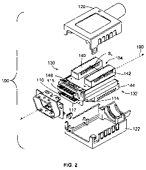
[0019] Figure 2 is a partially exploded view of the connector 100.
As shown, the connector 100 includes a pair of board assemblies 130 and 132
that are
configured to be enclosed by the housing shells 120 and 122 (i.e., within the
interior
of the connector 100) when the connector 100 is fully assembled. The housing
shells
120 and 122 may be manufactured (e.g., die-cast) from a metal material or a
nonconductive material. As shown, the board assembly 130 includes the circuit
board
-4-
CA 02768624 2012-01-19
WO 2011/019376
PCT/US2010/002196
114 and a pair of shielded terminal blocks 140 and 142 mounted to the circuit
board
114, and the board assembly 132 includes the circuit board 116 and a shielded
terminal block 144 mounted thereto. (Although not shown, the board assembly
132
may also include another terminal block mounted thereto.) In
alternative
embodiments, the board assemblies 130 and 132 may have only one or more than
two
terminal blocks mounted to each other. Furthermore, in alternative
embodiments, the
circuit boards 114 and 116 may sandwich one or more terminal blocks between
the
circuit boards 114 and 116. The sandwiched terminal block(s) may be mounted or
electrically connected to both circuit boards 114 and 116.
[0020] The terminal blocks 140 and 142 may be located proximate to
the loading end 104 and extend parallel to or along the central axis 190. As
shown,
the terminal blocks 140 and 142 may be separated or spaced apart from each
other by
a spacing SI. Also shown, the board assemblies 130 and 132 may be held side-by-
side (e.g., stacked) by a board frame 148. The circuit boards 114 and 116 may
also be
staggered so that the mating ends 115 and 117 are not aligned with each other.
[0021] Figure 3 is a rear exploded perspective view of the board
assembly 130 and is shown with reference to a longitudinal axis 290, a lateral
axis
292, and a vertical axis 294. In the illustrated embodiment, the longitudinal
axis 290
extends parallel to the central axis 190 (Figure 1) of the connector 100
(Figure 1). As
shown, the circuit board 114 has a length Li that extends between a loading
end 160
and the mating end 115 and a width W1 that extends between a pair of side
edges 204
and 206. The circuit board 114 also has opposing board surfaces 208 and 210
with a
thickness T1 of the circuit board 114 extending therebetween. Although the
circuit
board 114 is shown as being substantially rectangular, the circuit board 114
may have
other shapes in alternative embodiments.
[0022] As shown, the circuit board 114 has an array 215 of plated
thru-holes or vias 214 that are configured to receive and electrically engage
terminal
contacts 218. The array 215 may be configured to achieve a desired performance
for
the connector 100. For example, moving from the loading end 160 to the mating
end
115, the vias 214 may be staggered with respect to each other such that the
vias 214
-5-
CA 02768624 2012-01-19
WO 2011/019376
PCT/US2010/002196
alternate between a first lateral distance X1 and a second lateral distance X2
away
from the side edge 204. Furthermore, the vias 214 may be grouped in pairs 220.
The
vias 214 of one pair 220 may be separated from each other by a longitudinal
distance
Y1 and adjacent vias 214 of different pairs 220 may be separated from each
other by a
longitudinal distance of Y2. The distances X1, X2, Y1, and Y2 may be
configured to
achieve a desired performance for the connector 100. However, the array 215 of
vias
214 may have different configurations. For example, in an alternative
embodiment,
the vias 214 may be located on the circuit board 114 widthwise (i.e., along
the lateral
axis 292). The vias 214 may have other arrangements in order to achieve a
desired
performance. For example, the vias 214 may be arranged in rows and columns.
[0023] The mating end 115 includes a mating edge 202 having a
plurality of pads 212 that are located proximate thereto and on both surfaces
208 and
210. The pads 212 may be arranged in a predetermined array and configured to
engage mating contacts or beams of another electrical connector that mates
with the
connector 100. In addition, the pads 212 are electrically connected through
the circuit
board 114 to corresponding vias 214. In some embodiments, the circuit board
114
includes traces (not shown) that extend through the circuit board in
predetermined
patterns that are configured to tune the transmission of signals through the
connector
100. For example, the circuit board 114 may include non-ohmic plates, fingers,
and
the like that are configured to reduce return loss and/or compensate for
offending
crosstalk.
[0024] In alternative embodiments, the pads 212 (or the mating end
115) and the vias 214 are not directly connected through the circuit board
114. For
example, the connector 100 may be configured like an RJ-45 jack where each via
214
is electrically coupled to another plated thru-hole within the circuit board
114, which,
in turn, is coupled to a pin contact that engages a plug contact at a mating
end. As
such, the terminal blocks 140, 142, and 144 (Figure 1) are not required to be
mounted
to a circuit board that also directly engages a mating connector. Furthermore,
in other
embodiments, the connector 100 does not include the circuit board 114 and may
use,
alternatively, a non-conductive electrical component or body configured to
house
conductive pathways that interconnect the terminal contacts 218 and the pads
212 (or
-6-
CA 02768624 2012-01-19
WO 2011/019376
PCT/US2010/002196
other contacts configured to engage the mating connector). Accordingly, as
used
herein, an "electrical component" includes a circuit board and as well as
other bodies
formed from a non-conductive material that house conductive pathways.
[0025] Also shown in Figure 3, the terminal block 142 includes a
terminal base portion 230 and an organizer portion 232 having a body 234. The
base
portion 230 may be substantially rectangular and have a length L2 that extends
along
the direction of longitudinal axis 290 and a width W2 that extends along the
direction
of lateral axis 292. The width W2 may be configured to reduce or optimize
electrical
coupling between adjacent conductors. In other words, the width W2, as shown
in
Figure 3, may be reduced to limit a length of the conductors in which the
conductors
are not in a preferred arrangement (e.g., twisted pair arrangement).
[0026] The base portion 230 is configured to be mounted to the
circuit board 114 and to facilitate holding terminal contacts 218 in a
predetermined
orientation. As shown, the base portion 230 also has a mating side 235 that
includes a
plurality of contact slots 240A and 240B and shield slots 242. The contacts
slots
240A and 240B are configured to support the terminal contacts 218 therein, and
the
shield slots 242 are configured to support shields 246 therein. When the
terminal
block 142 is fully assembled, the organizer portion 232 is stacked onto the
mating
side 235 of the base portion 230. As shown, the base portion 230 may include
holes
248 along the mating side 235.
[0027] The contact slots 240A and 240B are located in
predetermined positions with the base portion 230. More specifically, the
contacts
slots 240 are positioned so that the terminal contacts 218 may electrically
engage with
the vias 214. As such, in the illustrated embodiment, the contact slots 240A
and 240B
have a staggered relationship similar to the vias 214. The terminal contact
218 may
be, for example, an insulation piercing contact (IPC). In other embodiments,
the
terminal contacts 218 may be an insulation displacement contact (IDC).
Moreover,
the terminal contacts 218 may include tails or pin portions 219. In the
illustrated
embodiment, the contact slots 240 extend entirely through a thickness T2 of
the base
portion 230 so that the pin portions 219 of the terminal contacts 218 may be
inserted
-7-
CA 02768624 2012-01-19
WO 2011/019376
PCT/US2010/002196
into corresponding vias 214 to electrically and mechanically couple
corresponding
terminal contacts 218 and vias 214.
[0028] Figure 4 illustrates the organizer portion 232 in greater detail.
The body 234 of the organizer portion 232 has a length L3 that extends along
the
direction of the longitudinal axis 290, a width W3 that extends along the
direction of
the lateral axis 292, and a thickness T3 that extends along the direction of
the vertical
axis 294. The organizer portion 232 includes opposite mating and distal sides
250
and 253 and a loading side 252. The mating side 250 is configured to engage
the
mating side 235 (Figure 3) of the base portion 230 (Figure 3) when the
organizer
portion 232 is stacked with respect to the base portion 230. The loading side
252 has
a plurality of openings 254 that lead into corresponding channels 256 (shown
in
Figure 5). The channels 256 may extend in an axial direction from the loading
side
252 to the distal side 253. Each opening 254 may be configured to receive one
or
more conductors 276 (shown in Figure 5) and lead into one or more channels
256.
For example, each opening 254 shown in Figure 4 has a pair of opposing
protrusions
255 and 257 that are configured to hold separate two conductors 276 within a
common channel 256. The two conductors 276 may be from one differential pair.
The channels 256 may extend along the direction of the lateral axis 292
perpendicular
to the longitudinal axis 290. In some embodiments, the channels 256 may extend
substantially parallel to the board surface 208. Alternatively or in addition
to, the
channels 256 may extend substantially perpendicular to the slots 240. As
shown, the
organizer portion 232 may receive twelve total conductors 276. However, in
alternative embodiment, the organizer portion 232 may receive more or less
conductors 276.
[0029] The mating side 250 includes several openings 260 that lead
into corresponding passages 270 (shown in Figure 5). For instance, the mating
side
250 has several pairs of openings 260A and 260B. The openings 260A and 260B
are
configured to have a similar spatial relationship as the vias 214 (Figure 3).
For
example, the openings 260A and 260B may have a staggered relationship.
Furthermore, the mating side 250 may have a plurality of openings 262 that
lead into
corresponding passages 272 (shown in Figure 5). The passages 270 are sized and
-8-
CA 02768624 2012-01-19
WO 2011/019376
PCT/US2010/002196
shaped to receive the terminal contacts 218 (Figure 3) that project from the
mating
side 235 of the base portion 230, and the passages 272 are sized and shaped to
receive
the shields 246 (Figure 3) from the base portion 230. Also shown, the mating
side
250 may have guide posts 268 that project from the mating side 250 along the
vertical
axis 294. The guide posts 268 are sized and shaped to be received by the holes
248
(Figure 3) of the base portion 230.
[0030] Figure 5A is a cross-sectional view of the terminal block 142
taken along a plane that is parallel to the axes 290 and 292 (Figure 3) and
intersects
the channels 256. In the illustrated embodiment, the channels 256 are enclosed
such
that the conductors are surrounded by the body 234. The channels 256 may be co-
planar with respect to each other (i.e., extend along a common plane) and/or
oriented
in a common direction. However, the channels 256 may not be co-planar and may
be
oriented in different directions in alternative embodiments.
[0031] Figures 5B and 5C are cross-sections taken along a plane that
extends along the axes 292 and 294 (Figure 3). Figures 5B and 5C are through
adjacent passages 270A and 270B, respectively, of one channel 256. The base
portion
230 may have a mounting side 236 that is configured to be mounted on the board
surface 208 of the circuit board 114. The contact slots 240 may extend from
the
mounting side 236 therethrough. When the base portion 230 is mounted on the
board
surface 208, the board surface 208 and the mounting side 236 extend along an
interface I. In order to assemble the terminal block 142, the terminal
contacts 218
and shields 246 may be inserted into the corresponding contact slots 240 and
shield
slots 242 (Figure 4) within the base portion 230. The base portion 230 may
then be
mounted onto the circuit board 114 by inserting pin portions 219 of the
terminal
contacts 218 into corresponding vias 214. With respect to the organizer
portion 232,
the conductors 276 may be inserted into the openings 254 and advanced through
the
corresponding channels 256 for a predetermined length. With the terminal
contacts
218 and shields 246 projecting from the mating side 235 of the base portion
230 as
shown in Figure 3, the organizer portion 232 may be mounted or stacked onto
the
base portion 230. The terminal contacts 218 advance into the corresponding
passages
270 and electrically couple to the corresponding conductor 276.
-9-
CA 02768624 2012-01-19
WO 2011/019376
PCT/US2010/002196
[0032] However, in alternative embodiments, the terminal block 142
may be assembled by other methods. For example, the terminal contacts 218 and
the
shields 246 may first be inserted into the organizer portion 232 and then
lowered onto
the base portion 230 such that the terminal contacts 218 are inserted into the
corresponding contacts slots 240 and the shields 246 are inserted into the
corresponding shield slots 242.
[0033] As shown in Figures 5B and 5C, when the organizer portion
232 is engaged with the base portion 230, the mating sides 235 and 250 extend
along
an interface 12. In some embodiments, the mating sides 235 and 250 are
substantially
planar. However, in other embodiments, the mating sides 235 and 250 may not be
substantially planar and may (or may not) have complementary surfaces. Each
contact slot 240A aligns with a corresponding opening 260A of a corresponding
passage 270A, and each contact slot 240B aligns with a corresponding opening
260B
of a corresponding passage 270B. The terminal contacts 218 advance through
corresponding passages 270 when the organizer portion 232 and the base portion
230
are engaged. When the terminal contacts 218 reach the corresponding channels
256,
the terminal contacts 218 electrically couple or engage with the corresponding
conductor 276. For example, the terminal contact 218 may pierce or slice
through a
jacket of the conductor 276 and connect to a conductive core therein.
[0034] As shown, the terminal contact 218 within the passage 270A
electrically couples to the conductor 276A approximately at a point P1, and
the
terminal contact 218 within the passage 270B electrically couples to the
conductor
276B approximately at a point P2. The points P1 and P2 are separated from each
other
by the longitudinal distance Y1 and by a lateral distance X3. (The lateral
distance X3
is approximately equal to a difference between lateral distances X1 and X2
shown in
Fig 3.) Accordingly, two conductors 276 of one differential pair may be
engaged at
separate axial locations within one channel 256. Separating the points P1 and
P2 may
facilitate improving the performance of the connector 100 (Figure 1).
[0035] Furthermore, in the illustrated embodiment, the shields 246
are located within the passages 272. The passages 272 extend between adjacent
-10-
CA 02768624 2012-01-19
WO 2011/019376
PCT/US2010/002196
conductors 276 from separate differential pairs. The shield 246 may be sized
and
shaped to improve the performance of the connector 100. For example, the
shields
246 may be configured to reduce electromagnetic coupling between adjacent
conductors 276 and/or to dissipate heat generated by the conductors 276 within
the
channels 256. Accordingly, the distances X3 and Y1 and the shields 246 may be
configured for a desired performance.
[0036] Figures 6-8 illustrate alternative embodiments of terminal
blocks and board assemblies. Figure 6 is a perspective view of a terminal base
portion 330. The base portion 330 has a mating side 335 and a mounting side
336 that
is configured to be mounted onto a board surface of a circuit board (not
shown). The
base portion 330 also includes pairs 320 of contact slots 340 that are
configured to
hold terminal contacts 318. The contact slots 340 of each pair 320 are aligned
with
one another side-by-side (i.e., each contact slot 340 of one pair 320 is a
common
distance X4 or X5 away from a loading side 352 of the base portion 330). As
such, the
pairs 320 of the contact slots 340 are staggered along a length L4 of the base
portion
330.
[0037] Also shown in Figure 6, each pair of terminal contacts 318
may be separated by two shields 346. The shields 346 are sized and shaped to
prevent
electrical interference between adjacent pairs of terminal contacts 318. As
shown, the
terminal contacts 318 are similar to the terminal contacts 218, and the
shields 346 are
similar to the shields 246. However, other terminal contacts and shields may
be used.
Furthermore, although not shown, an organizer portion may have channels with
or
without passages leading into the channels that align with the terminal
contacts when
the organizer portion is mounted onto the base portion.
[0038] Figure 7 is a perspective view of a board assembly 430
formed in accordance with an alternative embodiment. The board assembly 430
may
have similar features as described above with respect to the board assembly
130. For
example, the board assembly 430 has a loading end 460, a mating end 415, and a
length L5 of a circuit board 414 extending therebetween. Furthermore, the
board
assembly 430 may include a pair of terminal blocks 442 and 443 that are
mounted
-11-
CA 02768624 2012-01-19
WO 2011/019376
PCT/US2010/002196
onto a board surface 408 of the circuit board 414. The terminal blocks 442 and
443
may each include a terminal base portion 431 and an organizer portion 432 that
facilitate electrically coupling terminal contacts 418 to conductors (not
shown). The
base portion 431 may have contact slots 440 and shield slots 444 configured to
hold
the terminal contacts 418 and shields 446, respectively.
[0039] However, as shown in Figure 7, the organizer portion 432
may include a mating side 450 that has open-sided channels 456 extending
therealong. The open-sided channels 456 may be configured to receive two
conductors, such as two conductors from a differential pair. The organizer
portion
432 also includes a loading side 452 having openings 454 therealong. In the
illustrated embodiment, the open-sided channels 456 are configured for an
interference fit with the corresponding conductors.
[0040] Also shown in Figure 7, the shields 446 may be substantially
cross-shaped and configured for an interference fit with the shield slots 444
and
corresponding passages (not shown) within the organizer portion 432. More
specifically, the shield 446 may include a laterally oriented base 448 and a
pair of
vertically oriented retention features 447 and 449. The retention features 447
and 449
may extend away from the base 448 in opposite directions with respect to each
other.
Also, the retention features 447 and 449 may extend substantially
perpendicular to the
base 448. As shown, the retention features 447 and 449 may be shaped to form
interference fits with the base and organizer portions 431 and 432. For
example, the
retention features 447 and 449 may include barbs 451 that project laterally
away from
the corresponding retention feature 447 or 449. As such, the shields 446 may
facilitate shielding and/or dissipating heat generated by the conductors and
may also
facilitate securing the base and organizer portions 431 and 432 together.
[0041] Also shown, when the terminal block 442 is fully assembled,
the loading side 452 of each terminal block 443 and 442 may be separated by
and face
each other across a spacing S2 along a width W4 of the board assembly 430. The
spacing S2 is sized so that a plurality of twisted pairs of conductors (not
shown) may
fit between the terminal blocks 443 and 442. In particular, the spacing S2 may
be
-12-
CA 02768624 2012-01-19
WO 2011/019376
PCT/US2010/002196
sized so that numerous differential pairs may be received along the board
surface 408
of the circuit board 414. The conductors may extend lengthwise along the
circuit
board 414 and then bend into the corresponding openings 454 along the loading
sides
452. Accordingly, the board assembly 430 may be configured to receive numerous
differential pairs and electrical engage the corresponding conductors to the
circuit
board 414.
[0042] Figure 8 illustrates a pair of board assemblies 530 and 531
that are coupled together by a board frame 502. The board assemblies 530 and
531
may have similar or identical elements and features and include circuit boards
514
and 513, respectively, with respective board surfaces 508 and 509. However,
the
board surfaces 508 and 509 may face away from each other in opposite
directions.
The board assembly 530 includes terminal blocks 541 and 542, and the board
assembly 531 includes terminal blocks 543 and 544. Each terminal block 541-544
includes an organizer portion 532 that has open-sided channels 556 extending
along a
mating side 550 of the organizer portion. Each open-sided channel 556 may be
configured for an interference fit with a corresponding conductor (not shown).
As
such, the organizer portion 532 can hold conductors therein during the
assembly of
the corresponding terminal block and the board assemblies 530 and 531 such
that the
conductors do not inadvertently fall out of the channels 556.
[0043] Each terminal block 541-544 may electrically couple twelve
conductors (not shown) to corresponding terminal contacts 518. The terminal
contacts 518 are shown as IDC' s in Figure 8 having eye-of-needle contacts
that form
an interference fit with corresponding vias 517. In the illustrated
embodiment, the
terminal contacts 518 are staggered with respect to each other and do not have
a
shield therebetween. Accordingly, the board assemblies 530 and 531 may be
coupled
together by the board frame 502 and inserted into an interior of a connector
housing
(not shown). The coupled board assemblies 530 and 531 may electrically
interconnect, for example, forty-eight (48) conductors from a cable.
[0044] In addition, many modifications may be made to adapt a
particular situation or material to the teachings of the invention without
departing
-13-
CA 02768624 2012-01-19
WO 2011/019376
PCT/US2010/002196
from its scope. For example, although Figures 3-8 show terminal blocks as
being
constructed by separate base portions and organizer portions, embodiments may
include terminal blocks that are integrally formed with the features of the
base
portions and organizer portions described above. Figure 9 illustrates such an
example
and, more particularly, a cross-section that is similar to the cross-sections
shown in
Figures 5B and 5C, except without the interface 12. As shown, a base portion
630 and
organizer portion 632 may be integrally formed into a terminal block 642
(e.g.,
through an injection molding process). As such, the base portion 630 is
positioned
between the organizer portion 632 and a circuit board 614, and the organizer
portion
632 extends away from the base portion 630 and the circuit board 614.
[0045] As shown in Figure 9, a terminal contact 618 may be inserted
through the bottom of the terminal block (i.e., through a mounting side 636
that
eventually forms an interface 13 with a board surface 608 of the circuit board
614).
Conductors 676 may be inserted into channels 656 before the terminal block 642
is
interfaced with the circuit board 614 along the interface 13 and before the
terminal
contacts 618 are inserted into the terminal block 642. After the conductors
676 are
inserted into the channels 656, the integrally formed terminal block 642 may
be
mounted on the board surface 608. Accordingly, a "base portion" and an
"organizer
portion" may be portions of a terminal block having one integrally formed body
or
may be separate components. Also, although not shown, the terminal block 642
may
include shield slots configured to form an interference fit with shields. The
shields
may be inserted into the terminal block 642 through the mounting side 636 or
any
other side of the terminal block 642.
[0046] In other alternative embodiments, the base portions and the
organizer portions may be integrally formed with other components of the
connector.
For example, the organizer portion 232 of Figure 3 may be integrally formed
with the
housing shell 120 (Figure 1). Furthermore, in alternative embodiments where
the
circuit board 114 is substituted with a plastic electrical component that
houses
conductive pathways, the base portion 230 may be integrally formed with the
plastic
component.
-14-