Note: Descriptions are shown in the official language in which they were submitted.
CA 02768750 2012-01-20
WO 2011/012171 PCT/EP2009/059973
1
CONFIGURABLE HYBRID CONVERTER CIRCUIT
The invention relates to a circuit for a
hybrid voltage source converter suitable for high
voltage direct current (DC) power transmission and
reactive power compensation.
In power transmission networks alternating
current (AC) power is typically converted to direct
current (DC) power for transmission via overhead lines
and/or under-sea cables. This conversion removes the
need to compensate for the AC capacitive load effects
imposed by the transmission line or cable, and thereby
reduces the cost per kilometer of the lines and/or
cables. Conversion from AC to DC thus becomes cost-
effective when power needs to be transmitted over a
long distance.
The conversion of AC power to DC power is
also utilized in power transmission networks where it
is necessary to interconnect the AC networks operating
at different frequencies.
In any such power transmission network,
converters are required at each interface between AC
and DC power to effect the required conversion, and one
such form of converter is a voltage source converter
(VSC).
Voltage source converters may employ
switches based on semiconductor technology that control
the flow of current. When combined with passive
components that provide temporary energy storage, the
ability of these switches to operate rapidly permits
CA 02768750 2012-01-20
WO 2011/012171 PCT/EP2009/059973
2
electrical power in practically any form to be
converted to a different form with minimal losses.
The emphasis on making such power
conversion efficient and compact has focused
development on increasing the frequency of operation so
that the size of the passive components can be reduced.
For power conversion equipment involving
high voltages, high frequency switching is not
desirable since it creates high stressing on
insulation, and series semiconductor switches must be
configured to operate within the operating parameters
of the poorest of the switches. The converter losses
therefore become exaggerated.
The size of the passive components in power
conversion equipment, such as capacitors and inductors,
are typically large to accommodate various tasks
including constraining of voltage variation and current
flow regulation. In addition the size of the power
conversion scheme may also be increased by the
provision of electrical insulation or protective
conductive shields around the converter for safety
purposes. The size and weight of converters also affect
the footprint of the HVDC station, which can be costly
due to the high costs of real estate.
It is known in voltage source converters to
use six-switch (two-level) and three-level converter
topologies 110,112 with insulated gate bipolar
transistors (IGBT) 114, as shown in Figures la and lb.
The IGBT devices 114 are connected and switched
together in series to enable high power ratings of 10's
to 100's of MW to be realized.
CA 02768750 2012-01-20
WO 2011/012171 PCT/EP2009/059973
3
This conventional approach may however
require a complex and active IGBT drive, and typically
requires large passive snubber components to ensure
that the high voltage across the series strings of IGBT
devices 114 shares properly during converter switching.
In addition, the IGBT devices 114 need to switch on and
off several times at high voltage over each cycle of
the AC supply frequency to control the harmonic
currents being fed to the AC network. These factors
lead to high losses, high levels of electromagnetic
interference and a complex design.
It is also known in voltage source
converters to use a multilevel converter arrangement
116 such as that shown in Figure 2. In such a
conventional multi-level converter 116 converter
bridges or cells 118 are connected in series, each cell
118 being switched at a different time.
The conventional multilevel converter
arrangement 116 eliminates the problems associated with
direct switching of series connected IGBT devices 114
because the individual cells 118 do not switch
simultaneously and the converter voltage steps are
comparatively small. Each cell 118 however requires a
large DC link capacitor 120 to carry fundamental
frequency and direct current components. Six DC side
reactors 122 are required to enable a parallel
connection and operation of converter limbs, and are
primarily used to limit transient current flow between
the converter limbs. These factors lead to expensive,
large and heavy equipment with significant amounts of
printed 14/06120 DESCPAMD' ET Uf S
Brtvalex Fax 0115638333 30 Mai 2011 15;73 P0118/016
PCT/EP 2009/059 973 - 30-05-2011
41? 35290 JL
4
stored energy. This makes pre-assembly, testing and
transportation of the equipment difficult.
WO 02/063758 discloses a voltage source
converter which, like all known voltage source
converters, has the ability to respond to an
Alternating Current (AC; side short circuit event. The
WO 02/063758 converter is able to switch its
serniconductor switches in order to reduce the converter
AC side terminal voltage to equal that of the AC
network attached thereto, and thereby limit and control
the fault current flowing into the converter.
Alternatively the WO 02/063758 converter may switch off
its semiconductor switches to block the flow of fault
current into the converter. Under such circumstances
the WO 02/063758 converter acts as a diode rectifier
with the Direct Current ;DC) side voltage being higher
than the AC side voltage, i.e. with the diode
associated with each of the semiconductor switches
being reversed biased, and so the fault current is
extinguished.
DE 195 35 552 Al discloses a self-
commutated inverter with capacitive store arrangement
having its fundamental power yield increased by
incorporating a device whereby the outputs of the
inverter are provided with the device which has per
phase at least cre single-phase cascade consisting of a,
capacitive store and a switching device, with which the
capacitive store can be connected into cx disconnected
from the phase at will. The switching devices used with
the inverter and device may comprise GTO thyristors.
is 30.05.2011 16:22:33 - 30.05.2011 16:24:16. This page 8 of 1fAMENDED SHEET
311 16:23:32
;eived at the EPO on May 30, 2011 16:24:16. Page 8 of 16
30/x5/20.11
CA 02768750 2012-01-20
Printed: 1"O/20,J1 DESOPAMD EF?2 p 599
Brevai x Fax 018639333 30 Mai 2011 15;23 PO09/016
'PCT/EP 2009/059 973 - 30-05-2011
SF 35290 JL
4a
DE 101 03 031 Al dicloses a current +
rectification circuit comprising single or multi-phase
voltage source inverters haying switchable energy
stores comprising unipolar capacitors which can take up
energy during overvoltage conditions. and prevent short
circuits and other uncontrolled energy emission. A
current rectification circuit comprising single or
multi-phase voltage source conxrerters has phase blocks
replaced by connection-compatible tripolar units
comprising switchable internal energy stores in the
form o unipolar capacitors so that energy is taken up
during overvoltage conditions and urncontro=led energy
emissions, especially short circuits, are prevented and
a given capacitance between the' P and N terminals and
the energy content of the substitute units can be
established.. This document also discloses a process for
controlling the circuit above-
WO 2007/029 349 relates to a device for
electron energy transfer which comprises at least one
current converter. Every current converter has phase
elements with respective arrangements of circuit
elements that comprise at least two turn-off power
conductors each and at least-two free-wheeling diodes,
each connected in parallel thereto, and energy storing
means. The aim of the invention is to improve the
transfer properties in or between power distribution
networks. For this purpose, the device is provided with
means for controlling the current converter in such a
manner that epoch, amplitude and/or the instantaneous
values of an alternating current of a transfer network
that can be connected to tl',.e device and/or the direct
m: 30.05.2011 16:22:33 - 30.05.2011 16:24:16. This page 9 of 1EAMENDED
SHEETD11 16:23:39
ceived at the EPO on May 30, 2011 16:24:16. Page 9 of 16
3Q/05/20.11:
CA 02768750 2012-01-20
Printed... #161201 DESCPAMD
::1:'
Brevalex Fax 0145638333 30 Mai 2011 15:23 P010/016
PCT/EP 2009/059 973 - 30-05-2011
SP 35290 JL
4b
current of a direct current line that connects at least
one current converter to a direct current source,
and/or the direct voltage and he direct current can be
controlled by at least three interconnected current
converters.
G3 2 418 079 A discloses a high voltage
direct current (HVDC) installation operable as an HVDC
converter and convertible to operate as a static var
compensator (SVC), the installation comprising an AC
input; a DC output; first and second Graetz bridges
connected in parallel between the AC input and the DC
output such' that all of the thyristor levels of the
bridges are utilized, a switch circuit operable to
disconnect the DC output such that one or both of the
bridges forms a thyrista_ controlled reactor (TOR) and
a reduced number of the thyristor 'levels of the bridges
are utilized; and means to reduce the size of the input
voltage provides by the AC input when the DC output is
disconnected.
According to an aspect of the invention
there is provided a circuit for a hybrid voltage source
converter suitable. for high voltage DC power
transmission and reactive power compensation, the
circuit comprising an assembly of electrically
interconnected elements including a plurality of first
elements and a plurality of second elements, the
circuit further including AC terminals connectable, in
use, to an AC network and DC terminals connectable, in
use, to a DC network, characterized in that a first set
of the plurality of second elements is connected
between the AC terminals and the p=uralz 7y of first
on: 30.05.2011 16:22:33 - 30.05.2011 16:24:15. This page 10 of -AMENDED
SHEET2011 16:23:46
:ceived at the EPO on May 30, 2011 16:24:16. Page 10 of 16
3; CA 02768750 2012-01-20 .... 1 ~`
CA 02768750 2012-01-20
Pr1n d 14/06. C24. ?# E PAM ._P200 9`
Brevalex Fax 0145638333 30 Mai 2011 15:23 P011/018
SP 35290 JL PCT/EP 2009/059 973 - 30-05-2011
4c
elements and a second set of the plurality of second
elements interconnected between the plurality of first
elements and the DC terminals, the circuit allowing
each of the first and second elements being configured
to be bypassed, to bbe a'sconnected or to include a
circuit arrangement of one or more electronic
components to construct, in use, a hybrid voltage
source converter including at least one first element
and at least one second element and in which the
circuit arrangement included i a the or each first
eemen.t is different to the circuit arrangement
included in the or each second element.
The circuit of the invention facilitates
the creation of a voltage source converter structure in
which at least two different circuit arrangements are
connected to each other and therefore facilitates the
creation. of a hybrid structure having the different
advantages of the respective circuit arrangements. Such
advantages may include, depending on the actual circuit
arrangements employed, reduction in DC link
capacitance, reduction in DC side reactors,
simplification of series IGBT converter components and
reduction in energy losses.
The assembly of electrically interconnected
elements effectively defines a flexible circuit
ion: 30.05.2011 16:22:33 - 30.05.2011 16:24:16. This page 11 of 1AMENDED
SHEET?011 16:23:51
eceived at the EPO on May 30, 2011 16:24:16. Page 11 of 16
4 .30/05.f201.1.
Printed. 14/0612011 DEStPAMQ: 0EP90x97
13revalex Fax 0145638333 30 Mai 2011 15:23 P012/016
PCT/EP 2009/059 973 - 30-05-2011
SP 352.90 JL
structure for the construction of a hybrid voltage
source converter that allows a designer of such power
converters to include standard circuit arrangements in
selected elements whilst bypassing or disconnecting the
5 other elements, and therefore easily allows a variety
of different possible configurations of voltage source
converter to be produced.
The circuit of the invention therefore
provides an effective means for identifying the best
possible configuration for a particular power
conversion problem in that it allows a nix ber of
different configurations of voltage source converter to
undergo investigation, comparison and optimization
quickly. It therefore allows the time required tc
develop a converter design to be shortened.
The flexibility provided by the assembly of
electrically interconnected components allows a hybrid
voltage source converter including the circuit to cope
with the demands of different AC and DC networks.
This arrangement maximizes the flexibility
of the circuit in that it allows one or more second
ion: 30.05.2011 16:22:33 - 30.05.2011 16:24:16. This page 12 of AMENDED
SHEET2011 16:23:56
aceived at the EPO on May 30, 2011 16:24:16. Page 12 of 16
5: CA 02768750 2012-01-20 3QICl......ir2..1:
CA 02768750 2012-01-20
WO 2011/012171 PCT/EP2009/059973
6
elements to be included in the AC power lines and/or
the DC power lines.
To further maximize the flexibility of the
circuit, a third set of the plurality of second
elements is preferably interconnected between neutral
point connections defined by the second set of the
plurality of second elements and the DC terminals.
In embodiments of the invention each of the
first elements may be configurable to include a
plurality of semiconductor switches connected in
series.
Such an arrangement allows the
implementation of near zero voltage and or current
switching of the series connected semiconductor
switches in a hybrid voltage source converter, reducing
switching losses and simplifying the hardware required
to control dynamic and steady-state voltage sharing.
In other embodiments of the invention each
of the first elements may be configurable to include a
plurality of semiconductor switches connected to define
a multi-level converter element so as to allow the
creation of a multi-level converter without affecting
the other elements of the hybrid voltage source
converter.
Each of the second elements is preferably
configurable to include:
- at least one energy storage device to provide
a nominally fixed voltage source; and/or
- at least one module, the or each module
including an energy storage device connected
with at least one pair of semiconductor
CA 02768750 2012-01-20
WO 2011/012171 PCT/EP2009/059973
7
switches that are controllable, in use, to
provide a continuously variable voltage
source.
Preferably, in embodiments in which at
least one of the second elements is configurable to
include at least one module, the or each of the
respective second elements is configurable to include a
plurality of modules connected in series so as to
define a chain-link converter element.
In such embodiments the circulating path
for switching is contained within the module, which
provides minimum self-inductance and makes the
switching operation more efficient.
The or each module may include an energy
storage device connected in parallel with a pair of
semiconductor switches in a half-bridge arrangement to
define a 2-quadrant unipolar module that can develop
zero or positive voltage and can conduct current in
both directions.
In other embodiments, the or each module
may include an energy storage device connected in
parallel with two pairs of semiconductor switches in a
full-bridge arrangement to define a 4-quadrant bipolar
module that can develop zero, positive or negative
voltage and can conduct current in both directions.
The or each energy storage device may be
connected to an auxiliary power bus so as to enable
real power to be transferred into and out of the or
each energy storage device to maintain a voltage
balance.
CA 02768750 2012-01-20
WO 2011/012171 PCT/EP2009/059973
8
In other embodiments the or each energy
storage device may be connectable temporarily to an
external voltage source to reset the energy storage
device.
Preferably the or each energy storage
device is a capacitor, which can be charged to store
energy and inserted into circuit to provide a voltage
step.
In other embodiments, the or each energy
storage device may be a battery, a fuel cell, a photo-
voltaic cell or an AC generator-rectified source, each
of which allows power to be transferred into or out of
the energy storage device to maintain voltage balance.
The semiconductor included in any of the
first and second elements is preferably provided in the
form of an insulated gate-bipolar transistor, a gate
turn-off thyristor or a field-effect transistor.
The use of semiconductor switches in a
voltage source converter is advantageous because such
devices are small in size and weight, and have
relatively low power dissipation, which minimizes the
need for cooling equipment. It therefore leads to
significant reductions in power converter cost, size
and weight.
Preferred embodiments of the invention will
now be described, by way of non-limiting examples, with
reference to the accompanying drawings in which:
Figures la and lb show schematic
illustrations of two prior art voltage source
converters for HVDC power transmission;
CA 02768750 2012-01-20
WO 2011/012171 PCT/EP2009/059973
9
Figure 2 shows a schematic illustration of
another prior art voltage source converter for HVDC
power transmission;
Figure 3 shows a schematic illustration of
a circuit according to an embodiment of the invention;
Figure 4a shows a first element configured
to include semiconductor switches connected in series;
Figure 4b shows a first element configured
to include semi-conductor switches connected to form a
multi-level converter element;
Figure 5a shows a 2-quadrant unipolar
module;
Figure 5b shows a 4-quadrant bipolar
module;
Figure 6 shows a schematic illustration of
a second element configured to include a plurality of
modules connected in series to form a chain-link
converter;
Figure 7 shows synthesis of a 50Hz waveform
using the chain-link converter of Figure 6;
Figure 8 shows a first hybrid voltage
source converter constructed in accordance with the
invention;
Figure 9 shows a second hybrid voltage
source converter constructed in accordance with the
invention;
Figure 10 shows a third hybrid voltage
source converter constructed in accordance with the
invention;
CA 02768750 2012-01-20
WO 2011/012171 PCT/EP2009/059973
Figure 11 shows a fourth hybrid voltage
source converter constructed in accordance with the
invention; and
Figure 12 shows a fifth hybrid voltage
5 source converter constructed in accordance with the
invention.
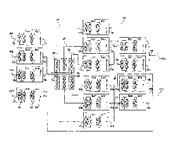
A circuit 22 for a hybrid voltage source
converter suitable for high voltage DC power
transmission and reactive power control is shown in
10 Figure 3. The circuit 22 comprises an assembly of
electrically interconnected elements, which include a
plurality of first elements, Elements 1 to 6 and a
plurality of second elements, Elements 7 to 20.
In the embodiment shown in Figure 3, the
first and second elements are interconnected to define
three converter limbs 24,26,28, each limb extending
between a first connection point 30 and a second
connection point 32.
More specifically, Elements 1, 2, 11 and 16
are connected in series between the first and second
terminals 30,32 of the first converter limb 24 so that
a first end 11a of Element 11 is connected to the first
connection point 30 and a second end llb of Element 11
is connected to Element 1. A first end 16a of Element
16 is connected to the second connection point 32 and a
second end 16b of Element 16 is connected to Element 2.
Elements 1 and 2 are connected to each other at a
midpoint 34 of the first converter limb 24, which is
also connected to a first end 9a of Element 9. A second
end 9b of Element 9 is connected to an AC terminal 36a
for connection to an AC network.
CA 02768750 2012-01-20
WO 2011/012171 PCT/EP2009/059973
11
Elements 3, 4, 12 and 15 are connected in
series between the first and second terminals 30,32 of
the second converter limb 26 so that a first end 12a of
Element 12 is connected to the first connection point
30 and a second end 12b of Element 12 is connected to
Element 3. A first end 15a of Element 15 is connected
to the second connection point 32 and a second end 15b
of Element 15 is connected to Element 4. Elements 3 and
4 are connected to each other at a midpoint 38 of the
second converter limb 26, which is also connected to a
first end 8a of Element 8. A second end 8b of Element 8
is connected to an AC terminal 36b for connection to an
AC network.
Elements 5, 6, 13 and 14 are connected in
series between the first and second terminals 30,32 of
the third converter limb 28 so that a first end 13a of
Element 13 is connected to the first connection point
30 and a second end 13b of Element 13 is connected to
Element 5. A first end 14a of Element 14 is connected
to the second connection point 32 and a second end 14b
of Element 14 is connected to Element 6. Elements 5 and
6 are connected to each other at a midpoint 40 of the
third converter limb 28, which is also connected to a
first end 7a of Element 7. A second end 7b of Element 7
is connected to an AC terminal 36c for connection to an
AC network.
The first connection point 30 of each of
the first, second and third converter limbs 24,26,28 is
connected to a first end 17a of Element 17. The second
connection point 32 of each of the first, second and
CA 02768750 2012-01-20
WO 2011/012171 PCT/EP2009/059973
12
third converter limbs 24,26,28 is connected to a first
end 20a of Element 20 of Element 20.
Elements 17, 18, 19 and 20 are connected in
series so that a second end 17b of Element 17 is
connected to a second end 18b of Element 18, a second
end 18a of Element 18 is connected to a first end 19a
of Element 19 and a second end 19b of Element 19 is
connected to a second end 20b of Element 20.
A first DC terminal 42a is connected to a
midpoint 44 between Elements 17 and 18 and a second DC
terminal 42b is connected to a midpoint 46 between
Elements 19 and 20.
The final element, Element 10, is connected
between an AC terminal 36d and a midpoint 48 between
Elements 18 and 19, the first end 10a of Element 10
being connected to the midpoint 48 and the second end
10b of Element 10 being connected to the AC terminal
36d.
The circuit 22 therefore includes:
- a first set of second elements, Elements 7 to 9
connected between the AC terminals 36a-36c and
an AC side of the first elements, Elements 1 to
6;
- a second set of second elements, Elements 11 to
16 connected between a DC side of the first
elements, Elements 1 to 6 and a third set of
second elements, Elements 17 to 20; and
- a third set of second elements, Elements 17 to
20, connected between neutral point connections
30,32 of the second set of second elements,
CA 02768750 2012-01-20
WO 2011/012171 PCT/EP2009/059973
13
Elements 11 to 16, and the DC terminals
42a,42b.
During use of the circuit 22 to construct a
hybrid voltage source converter, each of the first and
second elements is configurable to be bypassed, to be
disconnected or to include a circuit arrangement of one
or more electronic components.
In the embodiment shown in Figure 3, each
of the first elements, Elements 1 to 6, is configurable
to include a plurality of series connected
semiconductor switches 50 (Figure 4a) and may allow the
implementation of near zero voltage and or current
switching of the semiconductor switches 50 in the
hybrid voltage source converter.
In other embodiments, each of the first
elements, Elements 1 to 6, may include a plurality of
semiconductor switches 52 (Figure 4b) connected to
define a multi-level converter element so as to allow
the creation of a multi-level converter without
affecting the other elements.
In the embodiment shown in Figure 3, each
of the second elements, Elements 7 to 20, is
configurable to include a fixed capacitor 54, one or
more unipolar modules 56 and/or one or more bipolar
modules 58
Referring to Figure 5a, a unipolar module
56 includes a capacitor 60 connected in parallel with a
pair of semiconductor switches 62 in a half-bridge
arrangement that can develop zero or positive voltage
and can conduct current in both directions.
CA 02768750 2012-01-20
WO 2011/012171 PCT/EP2009/059973
14
Referring to Figure 5b, a bipolar module 58
includes a capacitor 64 connected in parallel with two
pairs of semiconductor switches 66 in a full-bridge
arrangement that can develop zero, positive or negative
voltage and can conduct current in both directions.
It is envisaged that each of the second
elements is configured to include one or more fixed
capacitors 54 or a chain of series connected unipolar
modules 56 or a chain of series connected bipolar
modules 58.
It is also envisaged that each of the
second elements may be configured to include a
combination of fixed capacitors 54 and/or unipolar
modules 56 and/or bipolar modules 58 depending on the
power conversion requirements.
The use of a chain of series connected
unipolar or bipolar modules 56,58 allows the
incorporation of a chain-link converter 68 (Figure 6)
into the hybrid voltage source converter, the chain-
link converter 68 including a series of modules M1rM2,
M3....Mn that each include a charged capacitor 70 that may
be bypassed or connected in series in either a forward
or reverse direction using one or more pairs of
semiconductor switches 72 to yield a continuously
variable voltage source.
The circulating path for the semiconductor
switching is contained within each module M1rM2, M3....Mn
leading to minimum self-inductance and making the
switching operation more efficient.
The use of a chain-link converter including
a plurality of bipolar modules is exemplified in Figure
CA 02768750 2012-01-20
WO 2011/012171 PCT/EP2009/059973
7 in which a 50Hz power waveform is synthesized by
staggering the switching of the individual modules.
Although many switching operations are taking place,
they are contained within individual modules and the
5 number of switching operations may be as low as the
frequency of the power voltage.
Configuration of one or more of the second
elements to include a chain-link converter during
construction of a hybrid voltage source converter is
10 desirable because, in the event of a DC side fault
during use of the hybrid voltage source converter, the
chain-link converter may be used to create voltage
steps to oppose any driving voltage from the AC side of
the converter and thereby extinguish any fault current.
15 Preferably the semiconductor switches
50,52,62,66 are constructed from insulated gate bipolar
transistors, gate turn-off thyristors, field-effect
transistors or any similar self-commutated
semiconductor switch.
The first and second elements of the
circuit 22 are configurable during construction of a
hybrid voltage source converter so that at least one
first element, Elements 1 to 6, is connected to at
least one second element, Elements 7 to 20, and the
circuit arrangement included in the first and second so
connected elements are different.
A first hybrid voltage source converter 74
constructed using the circuit 22 shown in Figure 3 is
shown in Figure 8.
CA 02768750 2012-01-20
WO 2011/012171 PCT/EP2009/059973
16
The hybrid voltage source converter 74
includes three AC terminals 36a-36c and a pair of DC
terminals 42a,42b.
Each of the first elements included in the
circuit 22, Elements 1 to 6, is configured to include a
plurality of semiconductor switches 50 connected in
series.
Of the second elements included in the
circuit 22, each of Elements 11 to 16 is configured to
include a plurality of bipolar modules 58 connected in
series to form a chain-link converter 68 and each of
Elements 18 and 19 is configured to include a fixed
capacitor 54.
The other second elements included in the
circuit 22, Elements 7 to 10, 17 and 20 are configured
to be bypassed.
A second hybrid voltage source converter 76
constructed using the circuit 22 shown in Figure 3 is
shown in Figure 9.
The hybrid voltage source converter 76
includes three AC terminals 36a-36c and a pair of DC
terminals 42a,42b.
Each of the first elements included in the
circuit 22, Elements 1 to 6, is configured to include a
plurality of semiconductor switches 50 connected in
series.
Of the second elements included in the
circuit 22, each of Elements 7 to 9 is configured to
include a plurality of bipolar modules 58 connected in
series to form a chain-link converter 68 and each of
CA 02768750 2012-01-20
WO 2011/012171 PCT/EP2009/059973
17
Elements 18 and 19 is configured to include a fixed
capacitor 54.
The other second elements included in the
circuit 22, Elements 10 to 17 and 20 are configured to
be bypassed.
A third hybrid voltage source converter 78
constructed using the circuit 22 shown in Figure 3 is
shown in Figure 10.
The hybrid voltage source converter 78
includes three AC terminals 36a,36b,36d and a pair of
DC terminals 42a,42b.
Each of Elements 1 to 4 of the first
elements included in the circuit 22 is configured to
include a plurality of semiconductor switches 50
connected in series. The other first elements included
in the circuit 22, Elements 5 and 6, are configured to
be disconnected.
Of the second elements included in the
circuit 22, each of Elements 11, 12, 14 and 15 is
configured to include a plurality of bipolar modules 58
connected in series to form a chain-link capacitor 68
and each of Elements 18 and 19 is configured to include
a fixed capacitor 54.
Of the other second elements included in
the circuit 22, Elements 10, 17 and 20 are configured
to be bypassed and Elements 13 and 16 are configured to
be disconnected.
While the voltage source converter 78
includes three AC terminals 36a,36b,36d, it only
includes two active converter limbs 24,26, which may be
CA 02768750 2012-01-20
WO 2011/012171 PCT/EP2009/059973
18
connected to two phases of an AC network via two of the
AC terminals 36a,36b.
The third phase of the AC network is
connected via the other AC terminal 36d directly to the
DC side neutral point connection 46 between Elements 18
and 19.
The generation of voltage waveforms in the
first two active limbs 24,26 causes a similar voltage
waveform to be generated at the DC side neutral point
connection 48. As a result, the voltage source
converter 78 only requires the use of two converter
limbs 24,26 to provide power conversion between a DC
network and a three-phase AC network.
A fourth hybrid voltage source converter 80
constructed using the circuit 22 shown in Figure 3 is
shown in Figure 11.
The hybrid voltage source converter 80
includes two AC terminals 36a,36b and a pair of DC
terminals 42a,42b.
Each of Elements 1 to 4 of the first
elements included in the circuit 22 is configured to
include a plurality of semiconductor switches 50
connected in series. The other first elements included
in the circuit 22, Elements 5 and 6, are configured to
be disconnected.
Of the second elements included in the
circuit 22, each of Elements 18 and 19 is configured to
include a unipolar module 56, Element 18 including two
unipolar modules 56 and Element 19 including one
unipolar module 56.
CA 02768750 2012-01-20
WO 2011/012171 PCT/EP2009/059973
19
Of the other second elements included in
the circuit 22, Elements 8, 9, 11, 12, 15, 16, 17 and
20 are configured to be bypassed and Elements 7, 10, 13
and 14 are configured to be disconnected.
The voltage source converter 80 is suitable
for interconnecting a single-phase AC network and a DC
network. This shows that the circuit 22 is flexible
enough to provide different configurations of voltage
source converter for connection to three-phase or
single-phase AC networks.
In other embodiments it is envisaged that
the arrangement of fixed capacitors 54 and/or unipolar
modules 56 and/or bipolar modules 58 in Elements 18 and
19 may be varied without affecting the functionality of
the voltage source converter. For example, in a variant
of the voltage source converter 80 shown in Figure 11,
two unipolar modules 56 may be included in Element 19
and one unipolar module 56 may be included in Element
18. It is also envisaged that in other variants all of
the unipolar modules 56 may be included in one of
Elements 18 and 19 with the other of Elements 18 and 19
being bypassed.
In other embodiments, where a DC mid
(neutral) point is required between Elements 18 and 19,
an equal number of fixed capacitors 54 and/or unipolar
modules 56 and/or bipolar modules 58 may be included in
each of Elements 18 and 19 so that Elements 18 and 19
contain equal and balanced arrangement of electronic
components.
Each of the voltage source converters
74,76,78,80 shown in Figures 8 to 11 may be
CA 02768750 2012-01-20
WO 2011/012171 PCT/EP2009/059973
controllable, in use, to produce desirable results in
the conversion of power between AC and DC networks. For
example, the semiconductor switches may be controllable
to switch at low frequency, giving a low-loss converter
5 design. In addition, harmonic components may be
deliberately created to control harmonic voltages and
currents on both the AC and DC sides of the converter.
Other configurations of voltage source
converter may be created by modifying the electrical
10 components that each of the first and second elements
is configurable to include.
Net real power may be transferred into or
out of the capacitors in some configurations when
unipolar modules 56 or fixed capacitors 54 are used on
15 the DC side of the converter when the direction of the
current cannot be switched. The transfer of real power
causes continuous charging or discharging of the
capacitors 60 of the unipolar modules and the fixed
capacitors 54 leading to an unsustainable converter
20 operation.
In order to mitigate this effect, an
auxiliary power bus may be provided and a voltage
source converter 82 including an auxiliary power bus 84
is shown in Figure 12.
The voltage source converter 82 is
essentially the same as the voltage source converter 74
shown in Figure 8 except that each of Elements 11 to 16
is configured to include a plurality of unipolar
modules 56, in place of bipolar module 58, connected in
series to form a chain-link converter 68.
CA 02768750 2012-01-20
WO 2011/012171 PCT/EP2009/059973
21
The capacitor 60 of each of the unipolar
modules 56 is connected to a first winding 86 of a
transformer arrangement 88 via a DC to AC inverter 90.
A second winding 92 of the transformer arrangement 88
is connected to the auxiliary power bus 84.
The electrical connection of the auxiliary
power bus 84 to the individual capacitors 60 allows
real power to be transferred between the capacitors 60
and the auxiliary power bus 84 to maintain voltage
balance in the capacitors 60.
Another option for mitigating the effect of
the transfer of net real power is to reset any fixed
capacitors 54 or the capacitors 60 of an unipolar
modules 56 through temporary connection, in use, to a
voltage source. For example when a voltage source
converter is connected between an AC network and a DC
network, the capacitors may be temporarily connected to
the DC network so as to restore the voltage balance in
the capacitors and prevent long term voltage drift.
A further option for mitigating the effect
of the transfer of net real power is to use real power
sources, such as batteries, fuel cells, photovoltaic
cells or AC generater-rectified units, instead of
capacitors.