Note: Descriptions are shown in the official language in which they were submitted.
CA 02771787 2012-02-21
1
DESCRIPTION
TITLE OF THE INVENTION CONTACTLESS COMMUNICATION MEDIUM
TECHNICAL FIELD
[0001] The present invention relates to a contactless communication
medium.
BACKGROUND ART
[0002] Conventionally, a technology of providing an antenna on a
substrate and
connecting the antenna to an IC module to form a contactless communication
medium such as an
IC card, an IC tag or the like which can perform data communication with an
external read/write
device is known.
CITATION LIST
[PATENT LITERATURE]
[0003] [PTL 1] Japanese Patent Publication No. 3721520
SUMMARY OF THE INVENTION
PROBLEMS TO BE SOLVED BY THE INVENTION
[0004] With the above-described conventional technology, when an inlet
including an IC
module mounted on an antenna sheet which has an antenna is combined with an
insulating
substrate or the like and the resultant assembly is used as a contactless
communication medium,
the substrate is made thick due to the thickness of a mold part or the like
containing an IC chip
sealed therein. Therefore, the inlet including the IC module mounted on the
antenna sheet is
combined with an inlay substrate having an opening in positional
correspondence with the mold
part so that the mold part is exposed from the opening.
[0005] In an IC card or the like, the outermost layer of the inlay is
held between
insulating resin substrates in a laminated manner; thus no serious problem
occurs even with the
above-described structure. However, especially, in the case where the inlay is
in the outermost
layer and thus the IC module part is exposed to the outermost layer, as in an
electronic passport
or the like, or in the case where the inlay is covered merely with a paper
material or the like
which is weak against electricity, the IC module is likely to be influenced by
an external impact
or the like. This causes malfunction or communication disorders of the
contactless
communication medium.
[0006] The present invention, made in order to solve the above-described
problems, has
an object of providing a contactless communication medium for reducing the
influence of an
CA 02771787 2012-02-21
= =
2
external impact or the like on an IC module and thus reducing the possibility
of malfunction or
communication disorders, even with a structure in which a mold part of the IC
module is
exposed from an opening provided in a substrate of the inlay.
SOLUTION TO THE PROBLEMS
[0007] To achieve the above objects, a contactless communication
medium according to
the present invention comprises a first substrate, a second substrate, an
antenna formed on the
second substrate, and an IC module connected to the antenna. The IC module has
at least a lead
frame, an IC chip mounted on the lead frame, and a mold part for sealing the
IC chip; the first
substrate has an opening for exposing the mold part; the second substrate has
a hole or recessed
part for accommodating at least the mold part, the hole or recessed part
having an area size larger
than the mold part; a sealing member having an insulating layer and an
adhesive layer in a
stacked manner is located so as to cover the mold part, the sealing member
being bonded to the
mold part via the adhesive layer; and where the sealing member has a
transverse width x and a
longitudinal width y, the hole or recessed part of the second substrate has a
transverse width a
and a longitudinal width b, and the first substrate has a thickness of d, at
least one of expressions:
x < a + 2d ... (1) and
y < b + 2d ... (2)
is fulfilled.
[0008] In a contactless communication medium according to the present
invention, only
numerical expression (2) is fulfilled.
[0009] In a contactless communication medium according to the present
invention, the
sealing member further fulfills at least one of expressions:
x < a + 2d - 0.2 mm ... (3) and
y < b + 2d - 0.2 mm ... (4).
[0010] In a contactless communication medium according to the present
invention, only
numerical expression (4) is fulfilled.
[0011] A contactless communication medium according to the present
invention
comprises a first substrate, a second substrate, an antenna formed on the
second substrate, and an
IC module connected to the antenna. The IC module has at least a lead frame,
an IC chip
mounted on the lead frame, and a mold part for sealing the IC chip; the first
substrate has an
opening for exposing the mold part; the lead frame is connected at a
connection part of the
antenna provided on the second substrate; a sealing member having an
insulating layer and an
adhesive layer in a stacked manner is located so as to cover the mold part,
the sealing member
being bonded to the mold part via the adhesive layer; and the sealing member
is bonded to the
CA 02771787 2012-02-21
3
second substrate via the adhesive layer in one direction in which the IC
module and the antenna
are connected to each other, among two directions parallel to sides of the
mold part for sealing
the IC chip; and the sealing member is provided so as not to contact the
second substrate in the
direction perpendicular to the one direction.
[0012] In a contactless communication medium according to the present
invention, an
outer surface of the first substrate and an outer surface of the sealing
member are formed to be
generally flat.
[0013] In a contactless communication medium according to the present
invention, a step
between the outer surface of the first substrate and the outer surface of the
sealing member is 20
p.m or less.
[0014] In a contactless communication medium according to the present
invention, at
least one of the insulating layer and the adhesive layer of the sealing member
has a longitudinal
elastic modulus which is smaller than that of the mold part.
ADVANTAGEOUS EFFECTS OF THE INVENTION
[0015] According to the present invention, even in the case where the
mold part of the IC
module is exposed from the opening provided in the substrate of the inlay,
adverse influences
such as an external impact or the like on the IC module are reduced, and the
possibility of
malfunction or communication disorders is reduced.
BRIEF DESCRIPTION OF THE DRAWINGS
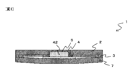
[0016] [FIG 1] FIG 1 is a cross-sectional view of an embodiment of a
contactless
communication medium according to the present invention.
[FIG 2] FIG 2 shows an embodiment of an IC module. Part (a) shows a plan
view, part (b) shows a cross-sectional view of part (a) as seen in an MD
direction, and part (c)
shows a cross-sectional view of part (a) as seen in a CD direction.
[FIG 3] FIG 3 shows an embodiment of an antenna sheet as a second substrate.
Part (a) shows a front surface, and part (b) shows a rear surface.
[FIG 4] FIG 4 provides cross-sectional views showing an example of form of a
sealing member. Part (a) shows a cross-sectional view as seen in the MD
direction, and part (b)
shows a cross-sectional view as seen in the CD direction.
[FIG 5] FIG 5 provides cross-sectional views showing an embodiment of a
sealing member according to the present invention. Part (a) shows a cross-
sectional view as
seen in the MD direction, and part (b) shows a cross-sectional view as seen in
the CD direction.
[FIG 6] FIG 6 provides cross-sectional views showing another embodiment of a
CA 02771787 2012-02-23
4
sealing member according to the present invention. Part (a) shows a cross-
sectional view as
seen in the MD direction, and part (b) shows a cross-sectional view as seen in
the CD direction.
[FIG 7] FIG 7 is a view illustrating expressions (1) through (4) according to
the
present invention.
[FIG: 8] FIG 8 provides cross-sectional views showing another embodiment of a
contactless communication medium according to the present invention. Part (a)
shows a cross-
sectional view as seen in the MD direction, and part (b) shows a cross-
sectional view as seen in
the CD direction.
[FIG 9] FIG 9 is a schematic view in the case where a contactless
communication medium according to the present invention is an electronic
passport.
DESCRIPTION OF EMBODIMENTS
[0017] Now, an embodiment of the present invention will be described
based on the
drawings.
FIG 1 is a cross-sectional view showing an example of a contactless
communication medium according to the present invention. As shown in FIG 1, a
contactless
communication medium 1 includes a first substrate 2, a second substrate 3, and
an IC module 4.
As described later, an antenna is formed on the second substrate and is
connected to the IC
module 4. The first substrate has an opening for exposing the IC module 4 and
a sealing
member is located so as to cover a mold part of the IC module.
[0018] The contactless communication medium 1 shown in FIG. 1 has a
structure in which
an antenna sheet as the second substrate 3 and an inlet including the antenna
and the IC module
are held between the first substrate 2 and an inlay sheet 7. The antenna sheet
has a hole, and
the IC module 4 is fit into the hole and connected to the antenna. In the
contactless
communication medium, the inlet is held between the inlay sheet and the first
substrate, and
these elements are bonded in a laminated manner and integrated. Thus, the
contactless
communication medium is formed to have a desired thickness.
[0019] For the first substrate 2 and the inlay sheet 7, for example, an
insulating plastic film
(PET-G: noncrystalline copolyester; PVC: vinyl chloride resin, etc.),
insulating synthetic paper
(polyolefin-based synthetic paper produced by PPG; trade name: "Teslin"
(registered trademark);
or polypropylene-based synthetic paper produced by Yupo Corporation; trade
name: "YUPO"
(registered trademark)) or the like is used. The plastic film mentioned above
is preferably a
flexible plastic film. Regarding the thickness, a material having a thickness
of, for example,
about 100 p.m to about 1000 gm, preferably about 100 gm to about 500 gm is
usable. Owing to
this, the material can fully exhibit functions as a substrate including a
strength and the like, and
CA 02771787 2012-02-21
also is provided with a sufficient flexibility and so is applicable to booklet-
shaped uses.
[0020] The opening of the first substrate 2 and the hole of the second
substrate 3 may be
formed by punching or the like. After the first substrate and the second
substrate are brought
together, the hole of the second substrate 3 may be sealed in a similar manner
to the opening of
the first substrate 2. For sealing, an insulating resin material or the like
is usable.
Alternatively, an adhesive such as a two-liquid curable epoxy resin or the
like is usable.
Especially where a shock-resistant elastic epoxy resin is used, the IC module
can be protected
against impacts.
[0021] For the sealing member 5 for covering the mold part, for example, a
resin tape
including an insulating layer and an adhesive layer is used. The insulating
layer has electric
insulation, heat resistance and moisture resistance. For the insulating layer,
resin materials such
as polyester-based resins, polypropylene-based resins, polyethylene-based
resins, polystyrene-
based resins, polyimide-based resins and the like are usable independently or
in a mixed state.
It is especially preferable to use a biaxially stretchable polyester resin. An
adhesive such as an
epoxy resin or the like is also usable. It is preferable that the insulating
layer have a dielectric
constant of, for example, about 1 to 5 ES.
[0022] For the adhesive layer, for example, a general viscous material such
as an acrylic-
based resin or the like is usable. The adhesive layer desirably has a
thickness of 20 gm or
greater in order to obtain a sufficient level of viscosity, but the thickness
may be appropriately
adjusted in consideration of the viscosity of the adhesive layer, the overall
thickness of the
sealing member and the like.
[0023] The sealing member 5 may have an overall thickness of about 25 pm to
100 lam,
and more desirably 80 pm or less, for the following reasons. When the resin
material is too thin,
the sealing effect is lowered. When the resin material is too thick, a step
may be caused when
the sealing member 5 is combined with the first substrate.
[0024] The sealing member 5 in this embodiment is formed such that an outer
surface of
the first substrate and an outer surface of the sealing member 5 are
continuous with each other
and are generally flat, and such that the outer surface of the sealing member
5 is generally flush
with the outer surface of the first substrate. Specifically, when the surfaces
are "generally flat"
or "generally flush", it is preferable that the step between the outer surface
of the first substrate
and the outer surface of the sealing member is 20 gm or less.
[0025] When a resin material is used for the sealing member 5, it is
preferable to use a
resin material having a longitudinal elastic modulus smaller than that of the
mold part 42 of the
IC module 4. When a resin tape including an adhesive layer is used for the
sealing member, it
is preferable to use a material in which at least one layer among the resin
material and the
CA 02771787 2012-02-23
6
adhesive layer has a longitudinal elastic modulus smaller than that of the
mold part of the IC
module.
[0026] FIG 2 shows cross-sectional views of the IC module 4 usable for the
present
invention. (a) of FIG. 2 is a plan view of the IC module in this embodiment,
(b) of FIG. 2 is a
cross-sectional view of (a) of FIG. 2 as seen in an MD direction and (c) of
FIG. 2 is a cross-
sectional view of (a) of FIG 2 as seen in a CD direction. CD and MD are two
directions
parallel to sides of the mold part.
As shown in (a) of FIG. 2 and (b) of FIG. 2, the IC module includes a lead
frame 43,
an IC chip 41 mounted on the lead frame, and the mold part 42 for sealing the
IC chip.
[0027] The lead frame is formed of, for example, a copper filament metal
film or the like
obtained by knitting copper filaments into a film form and plating the film
form with silver.
The lead frame includes a die pad 431 for supporting and fixing the IC chip
and terminal parts
432 connected to input/output pads of the IC chip.
[0028] The die pad 431 is formed to be larger by a certain degree than an
outer profile of
the IC chip 41, and is fixed to a bottom part of the IC chip. The die pad and
each terminal part
have a gap formed therebetween and are electrically insulated from each other.
The terminal parts are connected to the input/output pads (not shown) of the
IC chip
via bonding wires 44 of, for example, gold (Au) or the like.
[0029] The mold part 42 is formed of, for example, a resin material such
as an epoxy resin
or the like, and is formed so as to cover the IC chip, the input/output pads
of the IC chip, the
bonding wires, connection parts of the terminal parts and the bonding wires,
and the like. The
gaps between the die pad and the terminal parts are also filled with the mold
part. The IC
module is formed to have a thickness of, for example, about 0.3 mm.
[0030] FIG 3 shows an embodiment of the antenna sheet as the second
substrate. (a) of
FIG 3 shows a front surface of the antenna sheet, and (b) of FIG. 3 shows a
rear surface thereof.
The antenna sheet is formed of, for example, a flexible material formed of PEN
(polyethylene
naphthalate) or PET (polyethylene terephthalate). The thickness of the antenna
sheet is
appropriately selected from a range of, for example, about 0.02 mm to about
0.10 mm. The
antenna sheet shown in FIG. 3 is an example of an etched-type antenna formed
as an antenna 61.
On the front surface of the antenna sheet, the antenna 61 is formed, and on
the rear surface
thereof, a jumper wire 62 is formed.
[0031] The antenna 61 and the jumper wire 62 are electrically connected to
each other by
conduction parts 63 respectively provided therein. It is preferable to form
the conduction parts
to have a large area size so that the conduction is realized certainly with
such an arrangement.
The conduction of the antenna and the jumper wire is realized by, for example,
crimping
CA 02771787 2012-02-21
. =
7
processing of pressurizing and caulking the antenna and the jumper wire from
both sides and
breaking the antenna sheet, or by forming a through-hole and filling the
through-hole with a
conductive paste such as a silver paste or the like. There is no specific
limitation on the method
of conduction as long as the antenna and the jumper wire are physically or
electrically connected
to each other.
[0032] The antenna 61 has connection parts 64 formed to connect
the antenna 61 to the IC
module. It is preferable to form the connection parts to have a large area
size so that the
connection to the IC module is realized easily with such an arrangement.
However, the antenna
may be formed to have a shape corresponding to a communication characteristic
to be used by
the contactless communication medium. Depending on the type of the antenna,
the jumper wire
may need to be formed on the front surface of the antenna sheet or no jumper
wire may be
necessary. The shape of the antenna is not limited to that shown in FIG 3.
[0033] The antenna 61 and the jumper wire 62 are preferably, for
example, an etched-type
antenna formed by forming a thin film having a thickness of about 0.02 mm to
0.05 mm of
aluminum, copper, silver or the like on the front surface of the antenna
sheet, and patterning the
thin film by etching or the like. The reason for this is that when the inlet
is subjected to
repeated flexure, stress caused by the repeated flexure is applied to parts in
which the terminal
parts of the IC module are connected to the connection parts of the antenna
sheet, which
improves the flexibility of the etched-type antenna and prevents stress from
being concentrated
on a specific site. However, the antenna according to the present invention is
not limited to an
etched-type antenna, and may be an antenna of a wound coil formed of a
conductive wire, an
antenna provided with conductive ink by printing, or the like.
[0034] The antenna sheet has a hole 65 for accommodating the IC
module. This further
reduces and also uniformizes the thickness of the contactless communication
medium, prevents
action of a local stress, and improves the resistance against flexure. By
allowing even the lead
frame of the IC module to be accommodated in the hole, the IC module can be
fixed. In the
case where the parts of the antenna to be connected to the IC module are, for
example, increased
in area size and provided as the connection parts 64, the connection is
realized easily.
[0035] In FIG 3, the hole 65 has a size corresponding to the area
size of the module part,
but the present invention is not limited to this. In the case of, for example,
a coil antenna which
is connectable to the die pad without being fixed to the substrate, the hole
may have such a size
as to contain the die pad. Alternatively, connection parts with the antenna
may be provided on
the second substrate and thus the IC module may be directly mounted on the
second substrate
without forming the hole (see FIG 8 described later).
[0036] The connection parts 64 of the antenna desirably have a
width which is generally
CA 02771787 2012-02-21
,
=
8
equivalent to, or slightly smaller than, that of the terminal parts of the IC
module. Owing to
this, stress can be dispersed in the width direction and can be prevented from
being concentrated.
In addition, the connection parts of the antenna may be connected, with
certainty, over the entire
width of the terminal parts of the IC module, and so the reliability of the
antenna and the inlet
can be improved.
[0037] The connection parts 64 of the antenna desirably have a length
which is larger than
that of parts in which the terminal parts of the IC module overlap the
connection parts of the
antenna. Owing to this, edges of the terminal parts are connected so as to be
located at
generally central parts of the connection parts of the antenna, which are
internal to the ends of
the connection parts of the antenna. Therefore, the edges of the terminal
parts contact the
generally central parts of the connection parts of the antenna which have a
larger width than that
of the antenna coil.
[0038] On the rear surface of the second substrate, reinforcing
patterns (not shown) for
reinforcing the connection parts of the antenna may be formed in positional
correspondence with
the areas in which the connection parts of the antenna are formed. Owing to
this, the
connection parts of the antenna can be supported and reinforced both by the
second substrate and
the reinforcing patterns formed on the rear surface thereof.
[0039] Accordingly, when the parts in which the terminal parts of the
IC module and the
connection parts of the antenna are connected to each other are subjected to
repeated flexure, the
edges of the terminal parts can be supported by the generally central parts of
the connection parts
of the antenna having the larger width. Owing to this, the concentration of
stress on the antenna
can be prevented and so breakage of the antenna can be prevented.
[0040] Now, the sealing member will be described in more detail with
reference to FIG 4
and FIG. 5. In FIG. 4 and FIG 5, the contactless communication medium has a
structure in
which the antenna sheet as the second substrate and the inlet including the
antenna and the IC
module are held between the first substrate, the inlay sheet and a cover
sheet. In the contactless
communication medium shown in FIG 4 and FIG 5, the inlay sheet has a hole for
accommodating the IC module in order to reduce the thickness of the IC module
part, but the
present invention is not limited to this. The hole may be a recessed part.
[0041] It is desirable to combine the sealing member so as to cover a
part of the antenna
sheet in addition to the mold part as shown in (a) of FIG 4 and (b) of FIG 4,
because with such
an arrangement, the bonding strength of the IC module and the antenna sheet is
improved, and
especially in the CD direction, the bonding strength of the IC module and the
connection parts of
the antenna is improved. By contrast, because the sealing member covers a
large area, stress is
likely to be applied on the mold part in the MD direction when a line pressure
test is perfoimed
CA 02771787 2012-02-21
,
9
in the CD direction and stress likely to be applied on the mold part in the CD
direction when a
line pressure test is performed in the MD direction. This causes cracks.
[0042] The reason for this is as follows. When a line pressure is applied
from a bottom
surface of the IC module, a force of pressing the IC module upward is applied.
However,
where the sealing member is combined with the antenna sheet, there is no
escape of the force
because the antenna sheet is held between the first substrate and the inlay
sheet, etc. and is firmly
fixed. As a result, stress is applied on the mold part. By contrast, when ends
of the sealing
member are not in contact with the antenna sheet, the IC module is slightly
movable, and the
concentration of stress on the mold part can be prevented.
[0043] Thus, it is desirable that, as shown in (a) of FIG. 5, (b) of FIG.
5, (a) of FIG. 6 and
(b) of FIG. 6, the sealing member has a size by which the sealing member does
not contact the
antenna sheet in at least one of the MD direction and the CD direction.
FIG 5 shows a structure in which the ends of the sealing member are located
between the opening of the first substrate and side surfaces of the mold part.
By matching the
opening of the first substrate to the diameter of the mold part, the sealing
member is pressed by
inner side surfaces of the opening of the first substrate when the first
substrate is combined, and
is bonded to the side surfaces of the mold part. Thus, the ends of the sealing
member are fixed.
In FIG 6, the width of the hole of the second material is larger than the
diameter of the module
by a degree at which the ends of the sealing member do not contact the
substrate. Therefore,
the sealing member does not contact the antenna sheet.
In order to realize this structure, a sealing member fulfilling at least one
of:
x < a + 2d ... (1) and
y < b + 2d ... (2)
may be used where the transverse width of the sealing member (CD direction) is
x, the
longitudinal width of the sealing member (MD direction) is y, the transverse
width of the hole of
the second substrate is a, the longitudinal width of the hole of the second
substrate is b, and the
thickness of the first substrate is d (see FIG 7).
[0044] The conditions of (1) and (2) are provided in consideration that the
sealing member
is bonded to both side surfaces of the mold part by being pressed to both of
the side surfaces of
the mold part 42 by the inner side surfaces of the opening of the first
substrate. When these
conditions are fulfilled, a part of the sealing member which is not pressed by
the inner side
surfaces of the opening of the first substrate may be naturally hung, or a
part of the sealing
member may contact the side surfaces of the mold part because of some reason,
etc. When this
occurs, the sealing member is necessarily prevented from contacting the
antenna sheet. Even
taking a form of expanding in a horizontal direction, the sealing member does
not contact
CA 02771787 2012-02-23
antenna sheet (see FIG 6).
[0045] Therefore, when the sealing member 5 fulfilling at least one of
expressions (1) and
(2) is used, the sealing member can be prevented with certainty from
contacting the antenna
sheet in at least one of the MD direction and the CD direction. When a line
pressure test is
performed, generation of cracks due to the application of stress on the mold
part 42 can be
prevented.
[0046] At least one of (1) and (2) needs to be fulfilled, but it is
preferable to fulfill only the
condition of (2). The reason for this is that the sealing member is formed so
as to cover the
connection parts in the CD direction in which the IC module 4 and the antenna
are connected to
each other and so the sealing member is not bonded to the second substrate
(antenna sheet) 31 in
the MD direction perpendicular to the CD direction. The reason for this is as
follows. The
CD direction is the direction of the longer sides of the lead frame 43, and
the terminal parts are
formed so as to protrude from the mold part 42 and are connected to the
connection parts 64 of
the antenna at these sites. It is desirable to prioritize the secured
prevention of the invasion of
static electricity by covering the connection parts with the sealing member 5.
When the
condition in the MD direction is fulfilled, the generation of cracks in the
mold part can be
prevented when a line pressure is applied in the CD direction. Therefore, the
orientation of the
IC module 4 with respect to the contactless communication medium may be
determined where
the CD direction is a direction in which a line pressure is presumed to be
often applied due to
pressurization, etc. with a roller when, for example, the contactless
communication medium
passes through a machine during the production or actual use.
[0047] This condition is provided in consideration that the surface of the
first substrate 2
and the surface of the sealing member 5 are foinied to be generally flat, that
the thickness of the
sealing member is actually very thin as compared to the transverse width of
the mold part 42, etc.
although enlarged in the figure (for the sake of clarification), and the like.
[0048] Based on (1) and (2) mentioned above, precision of production
facilities will be
considered. Considering that the precision of combining the second substrate
31 with the IC
module 4 is generally 0.1 mm at the maximum and that the precision of
combining the sealing
member with the IC module is generally 0.1 mm at the maximum, the precision
of combining
the sealing member with the second substrate is 0.2 mm at the maximum.
[0049] Accordingly, it is preferable that the transverse width x and the
longitudinal width y
of the sealing member 5 further fulfill at least one of:
x < a + 2d - 0.2 mm ... (3) and
y < b + 2d - 0.2 mm ... (4).
Owing to this, even where the sealing member is combined with the second
CA 02771787 2012-02-23
11
substrate 31 with an offset of 0.2 mm at the maximum, the sealing member can
be prevented
with certainty from contacting the antenna sheet. Regarding expressions (3)
and (4), at least
one thereof needs to be fulfilled as in the case of expressions (1) and (2),
but it is more preferable
that only numerical expression (4) is fulfilled.
[0050] Where the width of the module in the CD direction is cd and the
width thereof in
the MD direction is md, the diameter of the module can be substituted into (1)
and (2) as follows
when there is no hole or when cd = a and md = b.
x < cd + 2d ... (1') and
y < md + 2d ... (2').
Similarly, where the width of the module in the CD direction is cd and the
width
thereof in the MD direction is md, the diameter of the module can be
substituted into (3) and (4)
as follows when there is no hole or when cd¨x and md=y.
x < cd + 2d - 0.2 mrn ... (3') and
y < md + 2d - 0.2 mm ... (4').
[0051] It is desirable that the sealing member 5 cover the entire outer
surface of the mold
part 42, or 90%, at the minimum, of both of the longitudinal width and the
transverse width of
the surface of the mold part. This is also applicable even where the sealing
member is
combined with an offset because of the lack of precision of production
facilities.
[0052] Now, the functions of this embodiment will be described.
In the contactless communication medium in this embodiment, as shown in FIG 1,
the opening for exposing the mold part 42 of the IC module 4 is formed in the
first substrate, and
the sealing member 5 including the insulating layer is combined so as to cover
the mold part.
Therefore, the occurrence of adverse influences due to the invasion of static
electricity on the IC
module part can be reduced.
[0053] By filling the gaps between the opening of the first substrate 2
and the mold part
with the sealing member 5, during a flatness test such as a ballpoint pen
test, a ballpoint pen is
prevented from being caught in the gaps. Thus, the flatness and smoothness of
the outer
surface of the contactless communication medium formed of the outer surface of
the first
substrate and the outer surface of the sealing member can be improved.
[0054] The sealing member 5 is disposed so as to cover the outer surface
of the IC module
4. In addition, the outer surface of the first substrate 2 and the outer
surface of the sealing
member are continuously formed to be generally flat and generally flush with
each other.
Therefore, even when a step is made between the outer surface of the first
substrate and the outer
surface of the IC module including the outer surface of the mold part 42, the
outer surface of the
first substrate and the outer surface of the sealing member can be generally
flush with each other.
CA 02771787 2012-02-21
ir '
12
Accordingly, the flatness and smoothness of the outer surface of the
contactless communication
medium formed of the outer surface of the first substrate and the outer
surface of the sealing
member can be improved.
[0055] The step between the outer surface of the first substrate 2
and the outer surface of
the sealing member 5 is 20 pm or less. Therefore, the outer surface of the
contactless
communication medium formed of the outer surface of the first substrate and
the outer surface of
the sealing member can be generally flat and flush with each other. The
criterion for passing a
flatness test such as a ballpoint pen test or the like can be fully satisfied.
The step is more
preferably 15 gm or less. Owing to this, the disorder ratio in the ballpoint
pen test can be made
generally 0%.
[0056] A resin tape is used for the sealing member 5. Therefore,
the positioning of the
sealing member is made easier, and so the production process of the
contactless communication
medium is simplified, the yield is improved, and the production cost is
reduced.
[0057] In the case where a resin tape, in which the insulating
layer or the adhesive layer
has a longitudinal elastic modulus smaller than that of the mold part 42 of
the IC module 4, is
used for the sealing member 5, the impact applied to the contactless
communication medium is
dispersed to the sealing member 5 as elastic energy. This provides an effect
of reducing the
impact applied to the IC module 4. The sealing member is elastically
deformable more easily
than the mold part of the IC module. Therefore, even when the outer surface of
the first
substrate is deformed and recessed by an external force received by the tip of
a ballpoint pen in a
ballpoint pen test, the sealing member is elastically deformed so as to reduce
the step between
the outer surface of the first substrate and the outer surface of the sealing
member while the tip
of the pen moves from a position on the outer surface of the first substrate
to a position on the
outer surface of the sealing member. Owing to this, stress in the advancing
direction of the tip
of the ballpoint pen, which is caused due to the step between the outer
surface of the first
substrate and the outer surface of the sealing member, can be reduced.
[0058] By limiting the size of the sealing member 5 to a size with
which the sealing
member 5 does not contact the second substrate in at least one of the MD
direction and the CD
direction, the generation of cracks caused by stress on the mold part 42
during a line pressure test
can be prevented. In the case where the size of the sealing member is
determined in
consideration of the offset which is caused by the precision of the production
facilities when, for
example, the IC module is combined with the second substrate or the sealing
member is
combined with the IC module, the sealing member can be prevented with more
certainty from
contacting the second substrate.
[0059] As described above, according to the contactless
communication medium of the
CA 02771787 2012-02-21
. ,
13
present invention, the invasion of the static electricity into the IC module
can be prevented, the
requirements regarding the flatness of the outer surface can be fulfilled, and
the generation of
cracks in the mold part can be prevented.
[0060] Now, a method for producing a contactless communication medium
according to
the present invention will be described.
Herein, a case of the contactless communication medium as shown in FIG 1
including a first substrate, an inlet including an antenna and an IC module
provided on an
antenna sheet as a second substrate, and an inlay sheet will be described.
[0061] Here, the contactless communication medium is produced as
follows. For
example, first, an IC module is located in a hole of the antenna sheet having
the antenna formed
thereon and is connected with the antenna, thus to form an inlet. A mold part
of the IC module
is covered with a sealing member. Next, this is held between the inlay sheet
and the first
substrate, and these elements are stacked such that the IC module is
accommodated in an
opening made in the first substrate.
[0062] Next, a pressing step of pressing the first substrate and the
inlay sheet from outside
so that the first substrate and the inlay sheet are mutually pressed is
performed. By this
pressing step, the first substrate, the inlet, the inlay sheet and the sealing
member in the opening
are compressed, and the outer surface of the first substrate and the outer
surface of the sealing
member are formed to be generally flat and generally flush with each other.
[0063] In the case where the synthetic paper as described above is used
for the first
substrate and the inlay sheet, the inlet, the first substrate and the inlay
sheet are bonded together
by an adhesive lamination method as follows. An adhesive is applied to the
antenna sheet of
the inlet or to a surface of the first substrate and a surface of the inlay
sheet which are to contact
the antenna sheet, and these elements are bonded together at a relatively low
temperature of, for
example, about 70 C to 140 C.
[0064] As the adhesive, for example, EVA (ethylene vinyl acetate resin)-
based, EAA
(ethylene - acrylic acid copolymerizable resin)-based, polyester-based,
polyurethane-based or
other adhesives are usable.
Instead of applying the adhesive, an adhesive sheet using any of the above-
mentioned resins usable as the adhesive may be held between the antenna sheet
and the first
substrate and between the antenna sheet and the inlay sheet.
[0065] In the case where a thermoplastic film is used for the first
substrate and the inlay
sheet, the inlet, the first substrate and the inlay sheet are bonded together
by a theimal lamination
method as follows. The inlet and the first substrate, and the inlet and the
inlay sheet, are
pressurized while being heated to a temperature exceeding the softening
temperature of the first
CA 02771787 2012-02-21
= '
14
substrate and the inlay sheet, for example, about 130 C to 170 C to cause melt-
bonding. Even
when the thermal lamination method is used, any of the above-mentioned
adhesives may also be
used in order to cause melt-bonding more certainly.
[0066] After the inlet, the first substrate and the inlay sheet
are bonded together, the
external shape of the integrated first substrate, inlay sheet and inlet is
processed into a desired
shape.
In this manner, the contactless communication medium shown in FIG 1 can be
produced.
[0067] In the above embodiment, the pressing step is introduced
for producing the
contactless communication medium, but the pressing step is not absolutely
necessary. Even
without the pressing step, the gaps between the IC module and the inner side
surfaces of the
opening of the substrate may be filled with the sealing member. The outer
surface of the
substrate and the outer surface of the sealing member can be formed to be flat
by use of, for
example, a roller, a scraper or the like instead of the pressing step.
[0068] Here, regarding the softening temperature of the first
substrate and the inlay sheet,
the softening temperature of PET-G is about 105 C to 150 C, and the softening
temperature of
PVC is about 80 C to 100 C.
By contrast, the antenna sheet as the second substrate is formed of PEN or PET
as
described above in the embodiment. The softening temperature of PEN is about
269 C, and the
softening temperature of PET is about 258 C. Namely, the heat-resistant
temperature can be
increased as compared with the thermoplastic material conventionally used for
the antenna sheet
such as PET-G or the like having a low softening temperature.
[0069] Therefore, when the first substrate, the antenna sheet as
the second substrate, and
the inlay sheet are heated to about 130 C to 170 C, the first substrate and
the inlay sheet are
softened but the antenna sheet is not softened. Owing to this, even when the
antenna sheet is
heated while the inlet including the antenna sheet, the first substrate and
the inlay sheet are
stacked and bonded by the thermal lamination method, fluidization due to
plasticization can be
prevented. Accordingly, the movement of the antenna due to the fluidization of
the antenna
sheet can be prevented to improve the reliability of data communication.
[0070] Even if the antenna sheet is overheated to a temperature
exceeding the softening
temperature and as a result, is plasticized and fluidized, if the antenna coil
is forMed of an
etched-type antenna, the contact area size between the antenna and the antenna
sheet is increased,
and the fluidization resistance of the antenna can be increased. Therefore,
the antenna can be
prevented from moving along with the fluidization of the antenna sheet, and
the reliability of
data communication can be improved.
CA 02771787 2012-02-23
[0071] FIG 8 provides cross-sectional views of another structural example
of a contactless
communication medium according to the present invention. (a) of FIG. 8 is a
cross-sectional
view taken along a straight line crossing the IC chip in the CD direction. (b)
of FIG. 8 is a
cross-sectional view taken along a straight line crossing the IC chip in the
MD direction. FIG 8
shows a structure in which the second substrate 31 forming the antenna also
acts as an inlay
sheet. The second substrate does not have a hole, and the connection parts 64
of the antenna
are directly connected to the lead frame 43 of the IC module provided on the
substrate. In this case
also, a structure is preferable in which, as shown in the figures, the sealing
member is formed so
as to cover the connection parts in the CD direction in which the IC module
and the antenna are
connected to each other, and the sealing member does not contact the second
substrate (antenna
sheet) 31 in the MD direction perpendicular to the CD direction.
[0072] Now, an electronic passport will be described as an example of a
contactless
communication medium according to the present invention. As shown in FIG 9,
the electronic
passport has the above-described contactless communication medium as cover
sheets, and has a
booklet part 9 held between such cover sheets. To one surface of the
contactless
communication medium, a cover material acting as the cover sheet of the
electronic passport is
bonded.
[0073] An inlay sheet is provided in a layer below the antenna sheet as the
second
substrate of the contactless communication medium, and in a layer below this
layer, a sheet
bonded with the cover sheet is used. Owing to this, the external appearance
and the feel of the
electronic passport provided with the contactless communication medium can be
made
equivalent to those of a conventional passport. The contactless communication
medium
prevents the invasion of static electricity and has an improved flatness of
the outer surface.
Therefore, an electronic passport having a high reliability of data
communication, improved
easiness of writing letters and improved printability of stamps, and a good
external appearance
can be provided. In the case where only the cover sheet is used as the second
substrate and the
antenna is formed directly on the cover sheet, the contactless communication
medium can be
further reduced in thickness and provided with improved flexibility.
[0074] In the above embodiment, an electronic passport is described as an
example of the
contactless communication medium, but the contactless communication medium
according to the
present invention is usable for, for example, electronic ID documents, various
types of electronic
certificates of activity history, and the like other than the electronic
passports.
Example 1
[0075] As the first substrate, polyolefin-based synthetic paper having a
thickness of
178 p.m and including an opening at a position at which the IC module would be
located was
CA 02771787 2012-02-21
'
16
used. As the second substrate, an antenna sheet was used. As the inlay sheet,
polyoleftn-
based synthetic paper having a thickness of 178 p.m was used.
First, an IC module was fit into a hole of the antenna sheet including an
antenna
and the hole and the IC module was connected to the antenna to obtain an
inlet.
Then, an aqueous emulsion adhesive (EAA) was applied to the first substrate
and
the inlay sheet, and a sealing member formed of a resin tape was located on
the IC module of the
inlet so as to cover the mold part. The antenna sheet was held between the
first substrate and
the inlay sheet such that the IC module and the opening of the first substrate
would match each
other positionally, and these elements were combined and pressurized to obtain
a contactless
communication medium. For the sealing member, a resin tape including an
insulating layer
formed of a 25 m-thick polyester film and a 25 pm-thick adhesive layer
stacked on the
insulating layer was used.
[0076] With respect to the contactless communication medium in which
the mold part had
a size of 4.8 mm x 5.1 mm (longitudinal x transverse) and the hole of the
antenna sheet had a
size of 5.2 mm x 5.3 mm (longitudinal x transverse), the longitudinal width of
the sealing
member was varied to obtain samples 1-1, 1-2, 1-3, 1-4, 1-5 and 1-6. Regarding
the sizes of the
sealing members, 1-1 had a size of 8 mm x 13 mm, 1-2 had a size of 7 mm x 13
mm, 1-3 had a
size of 6 mm x 13 mm, 1-4 had a size of 5.5 mm x 13 mm, 1-5 had a size of 5 mm
x 13 mm, and
1-6 had a size of 4.5 mm x 13 mm.
[0077] The cross-section of each obtained contactless communication
medium was
measured with an electronic microscope. In any of samples 1-1 through 1-5,
there was no gap
between the inner side surfaces of the opening of the first substrate and the
mold part of the IC
module. Sample 1-6 was confirmed to have gaps at both ends of the sealing
member in the
longitudinal width direction. The total size of the gaps was 0.5 mm. In all of
samples 1-1
through 1-6, the step between the outer surface of the sealing member covering
the IC module
and the outer surface of the first substrate was 20 lam or less.
[0078] Next, a static electricity test was performed on the obtained
samples in conformity
with IS010373-7 and JIS X6305-7.
First, the direction of the longer side of the rectangle of the contactless
communication medium was set as the right-left direction, and the direction of
the shorter side
thereof was set as the up-down direction. Each sample was located such that
the first substrate
would be on top and the opening would be at the upper right corner of the
rectangle as seen in a
plan view. From the outer surface of the substrate having the opening,
voltages of +6 kV, -6 kV,
+8 kV and -8 kV were sequentially applied. Each time a different voltage was
applied, the
basic operation of the IC chip was confirmed, and the communication response
of the contactless
CA 02771787 2012-02-21
17
communication medium was measured.
[0079] The voltages for the sequential measurement were applied at
25 positions in total,
namely, 20 areas (position: 20) obtained by dividing a rectangular area which
was enclosed by
the antenna coil as an outer perimeter and was longer in the transverse
direction into 4 in the
longitudinal direction and into 5 in the transverse direction (4x 5), the
center of the mold part of
the IC module (position: center), a position on the substrate left to the
opening (position: left), a
position on the substrate right to the opening (position: right), a position
on the substrate upper to
the opening (position: upper), and a position on the substrate lower to the
opening (position:
lower).
[0080] The result of the measurements in the static electricity
test shows a good
communication response with all of samples 1-1 through 1-6, at all the
voltages and at all the
positions.
[0081] Next, a ballpoint pen test was performed on the samples. The
ballpoint pen test
was performed by allowing a ballpoint pen to run on the outer surface of the
first substrate in the
direction of the longer side of the antenna coil so as to pass over the IC
module. A
commercially available ballpoint pen having a diameter of 1 mm was used. The
ballpoint pen
was allowed to run at a load of 600 g and a rate of 25 mm/sec. After the
ballpoint pen was run
in a reciprocating motion 25 times, the basic operation of the IC chip was
confirmed, and the
communication response of the contactless communication medium was measured.
[0082] The result of the ballpoint pen test shows a good
communication response was
obtained with all of samples 1-1 through 1-6.
[0083] A stamp test was performed on the samples. The stamp test
was performed by
applying a load on the outer surface of the substrate having the opening using
a stamp.
The diameter of the tip of the punch of the stamp used was 10 mm. After an
impact of a load of 250 g was applied 50 times at a height of fall of 320 mm,
the basic operation
of the IC chip was confirmed, and the communication response of the
contactless
communication medium was measured.
[0084] The result of the stamp test shows a good communication
response was obtained
with all of samples 1-1 through 1-6.
[0085] A line pressure test in the CD direction was performed on
the samples. The line
pressure test was performed by orienting the sample such that the cover sheet
side of the sample
would contact a jig and the central position of the mold would be at the
central position of a side
= of the jig, and pulling the sample from an end thereof with a load.
The jig used was a right-angled metal jig having a width of 50 mm and r = 2.5.
After the sample was pulled at a load of 250 N, the basic operation of the IC
chip was confiimed,
CA 02771787 2012-02-23
=
18
and it was checked whether the mold part had been cracked.
[0086] The result of the line pressure test shows the mold part was
cracked in all of
samples 1-1 through 1-3.
[0087] In sample 1-4, the mold part was not cracked because the
longitudinal width of the
sealing member was shorter than a sum of the longitudinal width of the hole
and twice the
thickness of the first substrate and so basically the sealing member did not
contact the antenna
sheet. However, when a plurality of samples were created in similar conditions
and tested, it
was confirmed that the sealing member contacted the antenna sheet on rare
occasions depending
on the lack of precision of the production facilities and the mold part was
cracked because of this
influence.
[0088] In samples 1-5 and 1-6, the sealing member had a size in
consideration of the
precision of the production facilities, and the mold part was not cracked in
either of the samples.
[0089] <Comparative Example 1>
A sample was created in substantially the same method as in Example 1 except
that
the sealing member was not used.
[0090] The cross-section of each obtained contactless communication
medium was
measured with an electronic microscope. Gaps of about 50 ium were made between
the inner
side surfaces of the opening of the first substrate and the IC module, and the
step between the
outer surface of the mold part of the IC module and the outer surface of the
substrate having the
opening was larger than 20 Rm.
[0091] The above-described static electricity test was performed.
Communication
response disorders occurred at some of the voltages and at some of the
positions. The result of
the above-described ballpoint pen test shows communication response disorders
occurred. The
result of the above-described stamp test shows communication response
disorders occurred. By
contrast, the result of the line pressure test shows the mold part was not
confirmed to have been
cracked even though there was no sealing member.
[0092] Based on the above-described results, in this embodiment
using the sealing
member, the invasion of static electricity into the IC chip can be prevented.
By fulfilling the
flatness requirements on the outer surface, the occurrence of disorders in the
ballpoint pen test or
the stamp test can be prevented. In addition, the sealing member is prevented
from contacting
the second substrate, and thus the mold part can be prevented from being
cracked in the line
pressure test. By contrast, in Comparative Example 1 in which the sealing
member is not used,
the probability that the communication response disorders occur after each of
the tests other than
the line pressure test is very high.
CA 02771787 2012-02-21
19
DESCRIPTION OF THE REFERENCE CHARACTERS
[0093] 1 ... contactless communication medium
2 ... first substrate
3 ... second substrate (antenna sheet)
4 ... IC module; 41 ... IC chip, 42 ... mold part, 43 ... lead frame, 431 ...
die pad,
432 ... terminal part, 44 ... bonding wire
... sealing member
61 ... antenna, 62 ... jumper wire, 63 ... conduction part, 64 ... connection
part,
65 ... hole
7 ... inlay sheet
8 ... cover sheet
9 ... booklet part