Note: Descriptions are shown in the official language in which they were submitted.
CA 02772158 2014-07-11
54106-1069
- 1 -
Multifilament Conductor and Method for its Production
FIELD OF INVENTION
The present invention relates to a multifilament conductor
comprising a ribbon-shaped substrate and at least one
superconducting layer. The at least one superconducting layer
is formed on at least one surface of the ribbon-shaped
substrate and is subdivided into filaments. The ribbon-shaped
substrate has a first direction parallel to its longitudinal
extent and the at least one filament has a second direction
parallel to its longitudinal extent. The invention furthermore
relates to a method for producing such a multifilament
conductor.
BACKGROUND
Multifilament conductors comprising superconducting layers are
used, inter alia, as conductors in superconducting devices.
They may be used for example in superconducting windings of
magnetic resonance tomographs, in motors, in generators or in
current limiters. Particularly when using high-temperature
superconducting (HTS) materials, for example Y2BaCu307 (YBCO),
superconducting properties of the conductors are already
achieved at liquid nitrogen temperatures. Reliable and
economical superconducting devices can be produced in this way.
Second-generation (2G) industrial HTS conductors have a
monocrystalline HTS thin film, in particular made of ceramic
YBCO, as the current-carrying layer, which is formed on a
ribbon-shaped metallic carrier. In order to apply the
monocrystalline HTS thin film onto the carrier, the latter is
coated with a textured multicoat buffer layer onto which the
HTS layer is applied by deposition methods, for example
evaporation coating, laser deposition or chemical
decomposition.
CA 02772158 2012-02-24
PCT/EP2010/062285 - la -
2009P12615WOUS
On the HTS layer, a normally conducting protection or
stabilization layer is additionally applied, which
CA 02772158 2012-02-24
PCT/EP2010/062285 - 2 -
2009P12615W0US
can electrically bridge defects and short sections in the HTS
layer which have become normally conductive, and which protects
the HTS layer from mechanical damage. The normally conducting
layer generally consists of silver and/or copper. The ribbon-
shaped carrier, on which the layer stack of buffer, HTS and
stabilization layers is applied, generally has a width in the
millimeter or centimeter range.
In AC applications, a time-variant field component
perpendicular to the ribbon-shaped carrier is often
encountered. In the HTS layer, and to a lesser extent in the
stabilization layer as well, circulating shielding currents are
thereby induced which are superimposed on a transport current.
These shielding currents lead to electrical losses, which are
released in the form of heat and have to be dissipated from the
HTS conductors by a cooling device. Economical advantages by
saving energy which are achieved using HTS conductors, in
comparison with conventional ohmic conductors, are thereby
reduced or entirely negated.
Losses per length Ph/L are proportional to the alternating
field amplitude AB, frequency f, critical current Ic and
effective conductor width df perpendicular to the magnetic
field:
Ph/L = f x AB x 1c x df
In NbTi and Nb3Sn superconductors, the losses are reduced by
dividing the cross section into a plurality of thin filaments
with a small df, which are embedded in a metal matrix, for
example of copper. This measure, however, is only effective
when the conductor is twisted or stranded.
An application of this principle to HTS conductors is provided
by Roebel conductors. WO 03/100875 A2 discloses such a Roebel
conductor, which is constructed from a plurality of parallel
CA 02772158 2012-02-24
PCT/EP2010/062285 - 2a -
2009P12615W0US
HTS-coated ribbon-shaped carriers. Losses
CA 02772158 2014-07-11
54106-1069
3
= in a corresponding structure of an HTS conductor are determined
by the width of the individual ribbon. In order to further
minimize losses, it is known for example from US 2007/0191202
Al to subdivide the superconducting layer and the copper
stabilization layer into filaments by longitudinal grooves
parallel to the longitudinal direction of the ribbon-shaped
carrier. Methods for forming the longitudinal grooves or
trenches, extending as far as the carrier, include mechanical
treatment, chemical etching, laser processing, photoresist
techniques and local disruption of crystalline ordering. A
filament on a carrier is thereby subdivided into a plurality of
individual filaments, which extend parallel to the longitudinal
axis of the carrier. The width of the individual filaments on
the carrier is taken as the effective conductor width df,
rather than the width of the superconducting coated carrier as
a filament.
Although a reduction of the losses can be found in short
conductor samples, in long conductor portions, for example in
coil windings, the magnetic coupling between filaments is not
however eliminated and an external alternating field, as occurs
for example in coils, still induces large shielding currents.
The shielding currents may exceed the critical current density
of the superconducting material, so that the superconductor
enters the resistive state. Significant electrical losses are
incurred, which must in turn be dissipated in the form of heat.
SUMMARY
It is therefore an object of some embodiments of the present
invention to provide a multifilament conductor which presents a
further reduction of the electrical losses in comparison with
multifilament conductors known from the prior art. In
particular, it is an object of a multifilament conductor
according to some embodiments of the invention to minimize the
CA 02772158 2014-07-11
54106-1069
- 3a -
induction of currents in the multifilament conductor in
external alternating fields. It is a further object of some
embodiments of the present invention to provide a method for
producing a multifilament conductor, which presents minimal
electrical losses with minimized induction of currents in the
multifilament conductor in external alternating fields.
CA 02772158 2014-07-11
54106-1069
- 4 -
The multifilament conductor according to some embodiments of the
invention comprises a ribbon-shaped substrate and at least one
superconducting layer. The at least one superconducting layer
is formed on at least one surface of the ribbon-shaped
substrate and is subdivided into filaments. The ribbon-shaped
substrate has a first direction parallel to its longitudinal
extent and the at least one filament has a second direction
parallel to its longitudinal extent. The first direction of the
ribbon-shaped substrate makes an angle which is greater than
zero with the second direction of the at least one filament.
In this way, it is possible to effectively reduce the losses in
alternating-field applications and the influences of local
faults in industrial superconducting conductors, when using the
multifilament conductors for example in coils in which the
conductors are wound over one another. Particularly in bifilar-
wound coils, a significant reduction of the losses is achieved.
The losses Ph due to an alternating-field amplitude 8B
perpendicular to the multifilament conductor depend not on the
conductor width but on the width of the individual filaments. The
level of hysteresis losses is reduced by the factor df/b. In
magnetic applications, for example in nuclear spin tomography, in
nuclear magnetic resonance spectrometers and in accelerators, in
CA 02772158 2012-02-24
PCT/EP2010/062285 - 5 -
2009P12615WOUS
which a high field accuracy is required, the field defects
produced in the working volume by the smaller shielding
currents, which are localized to the filament width, are
significantly reduced.
An angle of between 30 and 60 degrees, in particular 45
degrees, between the first direction of the ribbon-shaped
substrate and the second direction of the at least one filament
is particularly advantageous. The at least one filament may be
formed fully along the second direction, in particular without
a length component parallel to the first direction. Length
components along the first direction increase the losses in
applications such as, for example, bifilar-wound coils.
The ribbon-shaped substrate may have a first surface on a front
side and an opposite second surface on a rear side, a plurality
of filaments being formed on both the first and second
surfaces. The filaments of the first surface may have a second
direction which is not equal to a third direction parallel to
the longitudinal direction of the filaments of the second
surface. A loss reduction effect similar to the reduction in
bifilar-wound coils is thereby achieved in the conductor.
Low-loss current conduction is in this case obtained
particularly with a transposed version of the conductor. To
this end, the at least one filament of the front side may be
electrically conductively connected to the at least one
filament of the rear side, in particular by means of at least
one layer which is formed on at least one third surface on one
or two side faces of the ribbon-shaped substrate. A
transposition length may lie in the region of 20 cm.
Bridging of defects in the superconducting layer may be carried
out particularly effectively, and losses thereby reduced
further, if at least one electrical bridge is formed between at
least two
CA 02772158 2012-02-24
=
PCT/EP2010/062285 - 6 -
2009P12615WOUS
neighboring filaments on one surface. An electrical connection
or electrical connections of the at least two neighboring
filaments are formed by the bridge or bridges. The at least one
electrical bridge may be arranged centrally on the one surface,
in particular with a longitudinal direction of the bridge
parallel to the one first direction of the ribbon-shaped
substrate. A defective filament with reduced local current-
carrying capacity is electrically bridged by the bridge and the
neighboring filament.
The multifilament conductor may comprise a layer stack
consisting of ribbon-shaped carrier material, at least one
buffer layer, at least one superconducting layer, in particular
a high-temperature superconducting (HTS) layer, and/or at least
one stabilization layer. The buffer layer makes an epitaxially
grown monocrystalline superconducting layer on the carrier
material possible. An HTS layer makes it possible to use the
multifilament conductor with superconducting properties even at
temperatures in the region of liquid nitrogen. The
stabilization layer protects the superconducting layer from
mechanical damage and electrically bridges local positions in
the superconducting layer with reduced current-carrying
capacity, i.e. it stabilizes and protects mechanically and
electrically.
The carrier material may consist of a metal, in particular
steel. The at least one buffer layer may comprise at least one
material from the group: Al, yttria, IBAD MgO, homo-epi MgO,
LMO, or combinations and/or alloys or layer stacks of these
materials. The at least one superconducting layer may consist
of YBCO. The at least one bridge may likewise consist of YBCO,
in particular the YBCO of the at least one HTS layer. This
allows loss-free electrical conduction even via the bridge. The
at least one stabilization layer may consist of copper or
silver or comprise a
CA 02772158 2014-07-11
54106-1069
- 7 -
layer stack with at least one copper and/or at least one silver
layer. The at least one bridge may also consist of or comprise
the material of the at least one stabilization layer, which
allows straightforward production of the bridge.
The carrier material may have a thickness in the range of from
50 to 100 pm and a width in the region of 10 mm. The at least
one buffer layer may have a thickness in the region of 100 nm.
The at least one superconducting layer may have a thickness in
the region of 1 pm, and the at least one filament may have a
width in the region of 0.5 mm. The at least one stabilization
layer may have a thickness in the range of from 3 pm to 300 pm.
These are favorable dimensions for a multiplicity of
applications of a multifilament conductor.
A method according to some embodiments of the invention for
producing the multifilament conductor described above comprises
the steps:
- two ribbon-shaped carrier materials are brought into
mechanical connection with one another via opposite sides
and
- at least one superconducting layer is respectively applied
on a side of a ribbon-shaped carrier material which lies
opposite the side of the mechanical connection, and
- a stabilization layer is applied onto the superconducting
layer,
- the stabilization layer of a first ribbon-shaped carrier
material being formed overlapping with the stabilization
= layer of a second ribbon-shaped carrier material at the
edges of the two ribbon-shaped carrier materials so that an
electrical connection of the stabilization layers is
established via the edges, and
- the superconducting layers and the stabilization layers
being subdivided into filaments.
CA 02772158 2012-02-24
PCT/EP2010/062285 - 8 -
2009P12615W0US
The two ribbon-shaped carrier materials may be brought
congruently into connection with one another. This method
allows straightforward and economical production of the
multifilament conductor in few steps.
The application of layers may be carried out by electrolysis,
soldering, evaporation coating, sputtering and/or thermal
decomposition of metal compounds in the vapor phase. The
subdivision of the superconducting layers and the subdivision
of the stabilization layers into filaments may be carried out
mechanically or by lasering and/or etching, in particular dry
or wet chemical etching, of trenches respectively passing fully
through a layer. Photolithography may in particular be used in
the etching method. Alternatively, the application of layers
may be carried out by printing or adhesively bonding the as yet
uncoated substrate ribbon at the position of the trenches.
During the subsequent deposition of superconductor and
stabilization layers, no material application takes place here
so that the desired filament structure is formed.
Trenches may be formed with a non-zero angle between the first
direction of the ribbon-shaped substrate and the second
direction of the at least one filament. The filaments on the
two ribbon-shaped carrier materials may be electrically
connected via their edges so as to form spiral-shaped current
paths.
The two ribbon-shaped carrier materials of the double-layered
substrate may be separated from one another by a heat-resistant
insulating interlayer or an air gap. This may, in particular,
be carried out by welding two ribbon-shaped carrier materials,
by folding a ribbon-shaped carrier ribbon into two ribbons
lying above one another, or by rolling a tube flat, in
particular before a step of texturizing rolling of the ribbon-
shaped carrier materials.
CA 02772158 2014-07-11
54106-1069
- 9 -
For the method according to some embodiments of the invention
for producing the multifilament conductor, the aforementioned
advantages associated with the multifilament conductor
according to some embodiments of the invention are achieved.
According to one aspect of the present invention, there is
provided a multifilament conductor comprising a ribbon-shaped
substrate and at least one superconducting layer, wherein the
at least one superconducting layer is formed on at least one
surface of the ribbon-shaped substrate and is subdivided into
filaments, and wherein the ribbon-shaped substrate has a first
direction parallel to its longitudinal extent and the at least
one filament has a second direction parallel to its
longitudinal extent, wherein the first direction of the ribbon-
shaped substrate makes an angle which is greater than zero with
the second direction of the at least one filament, and wherein
the angle between the first direction of the ribbon-shaped
substrate and the second direction of the at least one filament
lies between 1 and 5 degrees.
According to another aspect of the present invention, there is
provided a method for producing a multifilament conductor as
described above, wherein two ribbon-shaped carrier materials
are brought into mechanical connection with one another via
opposite sides with at least one superconducting layer
respectively being applied on a side of a ribbon-shaped carrier
material which lies opposite the side of the mechanical
connection and a stabilization layer being applied onto the
superconducting layer, the stabilization layer of a first
ribbon-shaped carrier material being formed overlapping with
the stabilization layer of a second ribbon-shaped carrier
CA 02772158 2014-07-11
54106-1069
- 9a -
material at the edges of the two ribbon-shaped carrier
materials so that an electrical connection of the stabilization
layers is established via the edges, and the superconducting
layers and the stabilization layers being subdivided into
filaments, wherein an angle between a first direction of the
ribbon-shaped substrate and a second direction of at least one
of the filaments lies between 1 and 5 degrees.
BRIEF DESCRIPTION OF THE DRAWINGS
Preferred embodiments of the invention, with advantageous
refinements will be explained in more detail below with the aid
of the following figures, but without being restricted thereto.
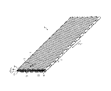
Fig. 1 shows a multifilament conductor in oblique view with
filaments parallel to the substrate axis, according
to the prior art, and
Fig. 2 shows the layer structure of a filament of a
multifilament conductor according to the prior art,
and
Fig. 3 shows a multifilament conductor according to the
invention comprising filaments which, obliquely on a
front and rear side of a substrate, are formed
extending spirally around its circumference, and
Fig. 4 shows a multifilament conductor similar to the one
shown in Fig. 3, bridges being formed between
neighboring filaments, and
Fig. 5 shows a plan view of the multifilament conductor
shown in Fig. 3, comprising filaments on the front
CA 02772158 2014-07-11
54106-1069
- 9b -
side (delimited by continuous lines) and rear side
(dashed lines), and
Fig. 6a shows a sectional view of the multifilament conductor
shown in Fig. 3, comprising two carriers placed in
direct connection, and
CA 02772158 2014-07-11
54106-1069
- 10 -
Fig. 6b shows a sectional view of the multifilament conductor
shown in Fig. 3, comprising a compressed tube as the
substrate, and
Fig. 6c shows a sectional view of the multifilament conductor
shown in Fig. 3, which consists of a folded-together
part as the substrate with a weld bead on the open
side.
DETAILED DESCRIPTION
Fig. 1 shows a section perpendicular to the longitudinal axis
of a multifilament conductor 1, in oblique view from the front
onto the multifilament conductor 1, according to the prior art.
The multifilament conductor 1 comprises a ribbon-shaped
substrate 2 having a front side 9 and a rear side 10. A first
direction 21 of the ribbon-shaped substrate 2 is defined as the
longitudinal direction of the ribbon-shaped substrate 2.
Parallel to the first direction 21, strip-shaped, mutually
parallel strips of a buffer layer 4 are applied on the front
side 21 of the ribbon-shaped substrate 2. The strips of the
buffer layer 4 are separated from one another, and have a
second direction 22 which corresponds to the longitudinal
direction of the strips of the buffer layer 4. A
superconducting layer 3, for example of YBCO material, is
formed on the strips of the buffer layer 4. A thin silver layer
(Ag layer) 5a and a copper layer (Cu layer) 5b is formed as a
support or stabilization layer 5 on the superconducting layer
3. Between the layer stacks or filaments 20, respectively
consisting of the buffer layer 4, the superconducting layer 3.
and the stabilization layer 5, through-trenches 6 are formed
for separating the filaments 20.
Under the action of a time-variant external magnetic field (B) 8 on
the multifilament conductor 1, currents I are induced in the
stabilization layer 5 and/or the superconducting layer 3. These
induced currents I flow in one half of the number of filaments 20
. with one current direction 7 and in the other half of the number of
filaments 20
CA 02772158 2012-02-24
PCT/EP2010/062285 - 11 -
2009P12615W0US
with an oppositely directed current direction 7'. The current
paths are closed at the conductor ends. The currents I
generally exceed the critical current of the filaments 20 and
drive the superconductor into the resistive state, so that
considerable ohmic losses occur. In an untwisted conductor
according to Fig. 1, these increase linearly with the total
ribbon width b, and the subdivision of the filaments 20 of
width df exerts no effect.
Fig. 2 represents the layer structure of a filament 20
according to the prior art in detail. A thin aluminum (Al)
layer 11 is applied as strips on the front side 9 of the
substrate 2, an oblique view of a sectional representation
along the strip being shown in Fig. 2. On the Al layer 11 is a
layer of yttria 12. A layer of IBAD magnesium oxide (MgO) 13
and an epitaxial homo-epi MgO layer 14 are deposited thereon.
An epitaxial LMO layer 15 is formed on the epitaxial homo-epi
MgO layer 14. These layers 11 to 15 together form the buffer
layer 4 and have an electrically insulating effect in relation
to the substrate 2. They are used as a monocrystalline-ordered
sublayer and lead to monocrystalline growth of the
superconducting layer 3, for example of YBCO, on the substrate
2 over the buffer layer 3.
A silver (Ag) layer 5a and a copper (Cu) layer 5b are formed on
the superconducting layer 3. These two layers form the
stabilization layer 5, which protects the superconducting layer
3 from mechanical damage and electrically bridges defects in
the monocrystalline superconducting material.
A further Cu layer may be formed as a second stabilization
layer 5' on the rear side 10 of the substrate 2.
The substrate 2 of the multifilament conductor 1 in Figures 1
and 2 consists of Hastelloy or steel, is 50 pm thick and
CA 02772158 2014-07-11
54106-1069
- 12 -
has a width of 10 mm. The filament 20 represented in Fig. 2
comprises a buffer layer 3 having a thickness of 100 rim, and
has a width of 0.5 mm. The superconducting layer 3 is 1 pm
thick and the stabilization layer 5 on the front side 9 of the
substrate 2 is formed 23 pm thick, with a 20 pm thick Cu layer.
The copper stabilization layer 5' on the rear side 10 of the
substrate 2 is 20 pm thick.
Fig. 3 represents a multifilament conductor 1
in oblique view from above. The substrate 2 of the
multifilament conductor 1 consists of Hastelloy or steel, is 50
pm thick and has a width of 10 mm. The filaments 20, 20' in
this exemplary embodiment are arranged on the substrate 2 with
a second direction 22, which constitutes the longitudinal
direction of the filaments 20, which makes a non-zero angle
with the first, the longitudinal direction 21 of the substrate
2. The superconducting filaments 20, 20' are respectively
arranged on a surface of a first carrier 16 and second carrier
17. The two carriers 16 and 17 are both in mechanical
connection with one another via their rear sides, which lie
opposite the surfaces comprising filaments 20, 20', but
electrically are essentially separated by an interlayer 29, the
touching rear sides being referred to below as the side of
mechanical connection 18. The two carriers 16 and 17 and the
interlayer 29 together form the ribbon-shaped substrate 2 of
the multifilament conductor 1,,
On a surface of the substrate 2, trenches 6 are respectively
formed passing fully through between the filaments 20, 20' so
that the superconducting layers 3 of two neighboring filaments
20, 20' are respectively electrically separated from one
another. The filaments 20 on the first carrier 16 are
respectively arranged so that they lie congruently above one
another at the edge 19 of the carrier 16 with the filaments 20'
of the second carrier 17 at the edge 19 of the carrier 16, 17.
During the deposition or formation of the stabilization layer 5
on the carriers 16
CA 02772158 2014-07-11
54106-1069
- 13 -
and 17, the material of the stabilization layer 5 is co-
deposited at the edge 19. In this way, the filaments 20 of the
carrier 16 are electrically connected to the filaments 20' of
the carrier 17 via this material. During the formation of the
trenches 6, these are likewise formed passing fully through the
material of the stabilization layer 5 at the edge 19, so that
filaments 20 and 20' lying above one another are electrically
connected to one another only at the edge 19.
The layer thicknesses and substrate widths 2 and filament
widths 20, 20' are the same as the thicknesses and widths
described above for the multifilament conductor 1 of Figures 1
and 2.
The angle of the filaments 20 on the front side 9 has the
opposite value to the angle of the filaments 20' on the rear
side 10. The value of the angle lies in the range of from 1 to
degrees and from -1 to -5 degrees, respectively.
Superconducting filaments 20, 20' with a limited length b,
which end at the edges 19 of the ribbon-shaped substrate 2, are
formed on the front and rear sides 9, 10. A stabilization layer
5, 5 of normally conducting material, for example copper,
which is in electrical connection with the superconducting
layer 3 of the filaments 20, 20' and can bridge the current at
a defective, normally conducting position of the
superconductor, is applied onto the superconducting filaments
20, 20'. At the edges 19 of the ribbon-shaped substrate 2, the
stabilization layer 5, 5' is formed so that the filaments 20,
20' of the front and rear sides 9, 10 are electrically
connected via a normally conducting layer.
In this way, one or more parallel spiral-shaped current paths,
which are superconductive except for short normally conducting
regions at the edges 19 of the ribbon-shaped substrate 2, are
formed around the ribbon-shaped substrate 2. Therefore, a thin-
film superconductor is produced
CA 02772158 2012-02-24
PCT/EP2010/062285 - 13a -
2009P12615W0US
having a "twist" known from conventional superconducting
technology in the form of parallel twisted superconductor
filaments, which present low losses in alternating-field
applications.
CA 02772158 2014-07-11
54106-1069
- 14 -
Fig. 4 represents an alternative exemplary embodiment of the
multifilament conductor 1. This multifilament conductor 1 is
similar to the multifilament conductor 1 represented in Fig. 3,
except for the additional formation of bridges 23 between
neighboring filaments 20, 20'. In terms of layer structure, the
bridges 23 are constructed similarly as in the filaments 20, 20'
of Figs 1 to 3, or they consist only of the stabilization layer 5
or of the stabilization layer 5 and the superconducting layer 3.
They are formed electrically conductively and can bridge defects
in the superconducting layer 3 of a filament 20, 20' via the
superconducting layer 3 of the neighboring filament 20, 20'. In
Fig. 4, the bridges 23 are arranged as a web centrally on the
surface of the substrate 2 along its first direction 21. As an
alternative, however, the bridges 23 may also be arranged at or
close to the edge 19. They may also be arranged not as a
continuous web, but alternating or irregularly on the surface
between two respectively neighboring filaments 20, 20'. In the
exemplary embodiment which is represented in Fig. 4, the width
= a of the bridges 23 is in the region of 1/20 of the length b of
a filament 20 or 20' on one side of the substrate 2. Depending
on the material and required current-carrying capacity, the
width of the bridges 23 may also have different values.
In multifilament conductors 1, the likelihood that a local weak
point in a filament 20 or 20' will reduce the current-carrying
capacity rises with increasing length and decreasing width. In
windings having a long lenth of the multifilament conductor 1,
the current-carrying capacity of the entire multifilament
conductor 1 with mutually insulated filaments 20 and 20' can
thus be greatly compromised. By arranging bridges 23 between
filaments 20 and 20', redistribution of the current from a
damaged filament 20 or 20' into neighboring filaments 20 or 20'
can take place. So long as the average distance between weak
points along the.filaments 20 or 20' is significantly greater
than the transposition
CA 02772158 2012-02-24
PCT/EP2010/062285 - 15 -
2009P12615W0US
length L, the total current will find enough intact current
paths and the critical total current is reduced only slightly
even in long multifilament conductors 1.
Fig. 5 shows a plan view of a multifilament conductor 1
corresponding to the embodiment represented in Fig. 3. It can
be seen that the second direction 22 of the filaments 20 on the
first carrier 16 (solid lines as delimitation in the width of
the filaments 20 in Fig. 5) is arranged at an angle to a third
direction 26 of the longitudinal extent of the filaments 20' on
the second carrier 17 (dashed lines as delimitation in the
width of the filaments 20' in Fig. 5). The filaments 20 and 20'
on the carriers 16 and 17 therefore form an angle. The angle
lies in the range of a few degrees. Nevertheless, other angles
may also be envisaged, as represented for example in Fig. 5.
Via the electrical connection at the edge 19, the filaments 20,
20' on the first 16 and second carriers 17 form a twisted or
transposed multifilament conductor 1. The filaments 20, 20' run
around the conductor in the shape of a spiral. For the losses
Ph due to an alternating-field amplitude AB perpendicular to
the multifilament conductor 1, it is no longer the conductor
width b as in the case of a conductor without filaments 20,
20', but rather the width df of the individual filaments 20,
20' which is crucial. The level of hysteresis losses is reduced
by the factor df/b. Owing to the transposition of the filaments
20, 20', losses due to shielding currents which are induced
between the filaments 20, 20' are also less than or equal to
zero, if the buffer layer 4 is insulated sufficiently from the
carrier 16, 17. The magnetic flux through the surface between
two arbitrary parallel filaments 20 or 20' respectively adds up
to zero following one revolution after a transposition length
L. The voltages induced between them, and therefore the loss-
generating eddy currents, are thus reduced effectively
irrespective of the total length of the multifilament conductor
1.
CA 02772158 2014-07-11
54106-1069
- 16 -
In Fig. 5, as a dot-and-dash line, an area A is indicated by
way of example which is enclosed by two arbitrary filaments 20
on the front side 9 or 20' on the rear side 10. With a field
component B perpendicular to the area A, a magnetic flux BxA
passes through the area A. An induced voltage U = % A dB/dt is
applied via each of the two intersection points 27, 28 of the
filaments 20, 20' of the front side 9 and rear side 10 of the
substrate 2. It is greatest in the middle of the conductor and
zero at the edge 19. An electrically insulating layer 29
between the first and second carriers 16 and 17 prevents
induced currents perpendicularly through the thin substrate 2
between filaments 20 and 20'. These currents would be
superimposed on the transport current in the filaments 20, 20'
and drive the filaments 20, 20' into the resistive, lossy
range, and additionally generate ohmic losses in the
substrate 2. With the electrically insulating layer 29, or
interlayer, between the first carrier 16 and the second carrier
17, magnetic coupling via the substrate 2 is prevented.
In magnetic applications in which a high field accuracy is
required, as is the case for example in nuclear spin
tomography, accelerators and nuclear magnetic resonance
spectrometers, the field defects thereby produced in the
working volume are reduced significantly owing to the smaller
shielding currents which are localized to the filament width.
The multifilament conductor 1 can therefore also be used in
critical direct-current applications.
In the case of normally conducting electrical contacts between
the filaments 20 and 20' via the edges 19, there is an ohmic
resistance Rn which is approximately equal to
Rn = pri n (dn + ds) (dn La),
where pn is the electrical resistivity, dn, ds are the
thicknesses of the normal metal layer and of the carrier 16,
17, Ln = df L / 2 b is the length of a bridge 23 in the first
CA 02772158 2014-07-11
54106-1069
- 17
direction 21 and df is the filament width. Two bridges 23 per
strand length L add up in each filament 20, 20' to an average
resistance per unit length of
<Rn> / 1 = p, n + ds) 2 b / (dn df L2).
With a large transposition length L, this resistance can become
very small. For example, for a multifilament conductor 1 with
b = 10 mm width, 0.3 mm total thickness, Ic = 300 A, 15 filaments
20, 20' of width df = 0.5 mm, an effective critical current
density in the multifilament conductor 1 of j, = 100 Aimm2, a
transposition or strand length of L = 20 cm, p = 2x10⁻⁹ Om in
copper at 77 K, and a thickness of the copper layer 5 and the
substrate 2 of d, = d, = 0.1 mm, the averaged ohmic resistance of
a filament 20, 20' through a copper bridge 23 is given by
<12,> / 1 = 12.5 pOhm/m .
With I = Ic/15 = 20 A in the filament 20, 20', the voltage drop
is 250 pV/m or 2.5 pV/cm. This is in the region of the 1 pV/cm
voltage drop with which the critical current is conventionally
defined in industrial superconductors.
Additional losses increase with the square of the current. At Ic
300 A, these are 75 mW per meter of multifilament conductor 1
or 250 mW per kiloampere-meter. Compared with conventional
solutions, a multifilament conductor 1 comprising HTS material
therefore gives an energy saving of 90% compared with ohmic
conductors consisting of copper. Magnetization losses Ph in the
superconducting material can be reduced by small filament widths
df, as already described. AC applications at 50/60 hertz can
therefore be carried out economically viably with the
multifilament conductors 1 in superconducting cables,
superconducting transformers, electrical machines comprising
superconductors and other applications.
CA 02772158 2012-02-24
PCT/EP2010/062285 - 18 -
2009P12615WOUS
Added to this, the one to two orders of magnitude higher
current densities which are possible are also an advantage over
conventional copper conductors.
Figs 6a to 6c show sectional representations of the
multifilament conductor 1 represented in Fig. 5 with different
embodiments of the connection 18 of the first and second
carriers 16 and 17 via at least one interlayer 29. The
filaments 20, 20' are constructed similarly to the above-
described filaments 20, 20' from a layer stack: buffer layer 4,
superconducting layer 3 and stabilization layer 5. Trenches 6
are respectively formed between neighboring filaments 20, 20'.
Filaments 20, 20' on the front side 9 and rear side 10 of the
substrate 2 are electrically connected to one another by the
stabilization layer 5 via the edge 19.
In Fig. 6a, the first carrier 16 and the second carrier 17 are
respectively connected to one another in an electrically
insulating fashion over the surface via their rear sides. The
connection may, for example, be carried out by adhesively
bonding the rear sides onto one another. A thermally insulating
layer may additionally be arranged between the carriers 16 and
17.
In Fig. 6b, the carriers 16 and 17 are formed by compressing a
tube 24 of substrate material 2. A thin insulating air gap,
which can also be used for cooling, may remain inside the tube.
For example, liquid nitrogen may be passed through this gap and
additionally cool the multifilament conductor 1 from the
inside.
In Fig. 6c, the first and second carriers 16 and 17 are formed
by folding together a wide carrier, with a width of the wide
carrier equal to 2 times the width of a carrier 16, 17, the
fold line extending in the middle of the wide carrier along its
CA 02772158 2012-02-24
PCT/EP2010/062285 - 18a -
2009P12615WOUS
longitudinal axis. The fold line forms an edge 19 of the
substrate 2, and
CA 02772158 2012-02-24
PCT/EP2010/062285 - 19 -
2009P12615W0US
a weld or adhesive bead 25 may connect the first and second
carriers 16 and 17 to one another in a mechanically stable
fashion along the opposite edge 19 of the substrate 2. When the
stabilization layer 5 is deposited and the trenches 6 are
formed, the filaments 20 of the first and second carriers 16
and 17 are respectively connected via the edges 19, in which
case, when the trenches 6 are also formed at the edge 19,
neighboring filaments 20 of a carrier 16 or 17 are respectively
electrically separated from one another at the edge 19. A
combination of the exemplary embodiments in Figs 6a to 6c with
the exemplary embodiment of Fig. 4 provides electrical
connection of filaments 20 on a carrier 16 or 17 via the
bridges 23.