Note: Descriptions are shown in the official language in which they were submitted.
CA 02772219 2012-11-28
METHOD AND APPARATUS FOR PROTECTING POWER SYSTEMS FROM
EXTRAORDINARY ELECTROMAGNETIC PULSES
FIELD OF THE INVENTION
[002] The present invention relates to a method and apparatus for
preventing
extraordinary electromagnetic pulses (EEMP) arising, for instance, from a
nuclear explosion
or solar storm, from reaching and rendering inoperative electrical components
of an
electrical power generation and distribution system. More particularly, an
extraordinary
electromagnetic pulse (EEMP) is defined as a transient pulse arising from
nuclear
explosions (NEMP), non-nuclear electromagnetic pulses (NNEMP) of sufficient
strength to
reach and render inoperative components of an electrical power system,
collectively
referred to as EMP, or geomagnetically-induced current (GIC) as a result of
coronal mass
ejections from solar storms. A further aspect of the invention relates to a
high speed current
shunt which may be used for detection of GIC pulses.
BACKGROUND OF THE INVENTION
[003] The vital nature of electrical power systems to modern society is
well
recognized. For instance, the Report of the Commission to Assess the Threat to
the United
States from Electromagnetic Pulse (EMP) Attack, Critical National
Infrastructures, US
Government Printing Office, April 2008, states at page 17:
The functioning of society and the economy is critically dependent upon the
availability of electricity. Essentially every aspect of American society
requires electrical power to function. Contemporary U.S. society is not
1
CA 02772219 2012-02-24
WO 2011/028300 PCT/US2010/026708
structured, nor does it have the means, to provide for the needs of
nearly 300 million Americans without electricity. Continued electrical
supply is necessary for sustaining water supplies, production and
distribution of food, fuel, communications, and everything else that is a
part of our economy. Continuous, reliable electrical supply within very
tight frequency boundaries is a critical element to the continued
existence and growth of the United States and most developed countries.
[004] The foregoing Commission Report further discusses the threat of attack
to
electrical power systems by an electromagnetic pulse arising from a nuclear
explosion,
and also refers to the naturally occurring threats to electrical power systems
from
geomagnetic storms. Commission Report at page18. As used herein, electrical
power
systems connotes systems for generating electrical power, transmitting that
power over
short to long distances and distributing that power to end users.
[005] Based on published empirical data, it is generally accepted that an EMP
event
can render various components of an electrical power system inoperative. Two
such
electrical components, electrical generators for producing electricity and
electrical
transformers for stepping up or stepping down voltage levels as required for
power
transmission or distribution, are obviously vital. If generators or
transformers cease to
operate, the power system fails and society as we know it ends. Both
components
require a long lead time to build (e.g., 3-5 years for transformers and up to
10 years for
generators) if the demand from them is normal; that is, if failures occur
after expected
product lifetimes. However, if the demand for generators and transformers
surge due
to their premature failure resulting from an EMP event, the lead time to build
them
increases even further and likely dramatically.
[006] It would therefore be desirable to provide a method for preventing
various forms
of EMP from reaching and rendering inoperative components of a power supply
system.
The various forms of EMP include an unwanted transient electromagnetic pulse
arising
from nuclear electromagnetic pulse events (NEMP), non-nuclear electromagnetic
pulse
(NNEMP) events creating a pulse with a rise time of less than 500 picoseconds
and a
field strength (e.g., in excess of 20 volts per meter) sufficient to reach and
render
inoperative components of an electrical power supply system as defined above,
or
geomagnetically-induced currents (GIC) arising from coronal mass ejections of
solar
storms or other EMP events. These EMID's are classified herein as
extraordinary
electromagnetic pulses (EEMP's).
CA 02772219 2012-02-24
WO 2011/028300 PCT/US2010/026708
[007] Another problem in the prior art relates to how to accurately measure
high-
speed current pulses, such as GIC. Prior art techniques for high speed current-
pulse
measurements are almost exclusively inferential. The U.S. National institute
of
Standard and Technologies (NIST) prefers direct measurements wherever possible
rather than inferential measurements. The numerical calculations associated
with
inferential measurement techniques increase the likelihood of errors in
correcting raw
data to inferentially arrive at an actual measurement. This is because the
numerical
calculations required are complex, there is an impetus to simplify the
calculations, a
process which almost always leads to the introduction of errors.
[008] There are three overriding reasons for having a high-accuracy high-speed
current shunt, as follows:
1. Provide real-time monitoring means to guide the manufacture of devices to
protect electrical components of a power system from EEMP events.
2. Provide high speed output for control circuitry.
3. Provide high speed output for system operator notification of an EEMP
event.
[009] Therefore, it would be desirable to provide a direct technique for
measurement
of high-speed current pulses.
SUMMARY OF THE INVENTION
[0010] One form of the invention provides a method and apparatus for
preventing an
extraordinary electromagnetic pulse from reaching and rendering inoperative an
electrical component of an electrical power system, wherein the component is
located
in a conductive path of the system that receives the pulse. The method and
apparatus
comprises the steps or means for detecting the presence of the pulse in the
conductive
path prior to the pulse reaching and rendering inoperative the electrical
component.
The pulse is diverted around the electrical component with a low inductance,
high
current capacity circuit relative to the electrical component before the pulse
can reach
and render the electrical component inoperative,
[0011] The foregoing method and apparatus prevents various forms of EEMP from
reaching and rendering inoperative components of a power supply system.
3
CA 02772219 2012-11-28
[0011a] Accordingly then, in one aspect, there is provided a method for
preventing
an extraordinary electromagnetic pulse from reaching and rendering inoperative
a
magnetic-winding containing electrical component of an electrical power
system, which
component is located in a conductive path of said system that receives said
pulse, the
method comprising the steps of: a) detecting the presence of said pulse in
said conductive
path prior to the pulse reaching and rendering inoperative said electrical
component; b)
diverting said pulse around the electrical component by creation of a low
inductance, high
current capacity short-circuit across the electrical component, so as to
thereby collapse the
magnetic field in said winding before the pulse can reach and render the
electrical
component inoperative; and c) said low inductance, high current capacity short-
circuit
comprising: i) a high-voltage cold-cathode field-emission vacuum electron tube
including
a cylindrical inner electrode, at least one cylindrical grid encircling the
inner electrode, and
a cylindrical outer electrode encircling the at least one grid; the inner and
outer electrodes
and the at least one grid sharing a common main axis; ii) the radial spacing
from either the
inner electrode or the outer electrode to an adjacent grid is such as to
create therebetween
a circular waveguide supporting the transverse electromagnetic mode.
[0011 b] In another aspect, there is provided an apparatus for preventing
an
extraordinary electromagnetic pulse from reaching and rendering inoperative a
magnetic-winding containing component of an electrical power system, which
component
is located in a conductive path of said system that receives said pulse, the
apparatus
comprising: a) means for detecting the presence of said pulse in said
conductive path prior
to the pulse reaching and rendering inoperative said electrical component; and
b) means
for diverting said pulse around the electrical component by creation of a low
inductance,
high current capacity short-circuit across the electrical component so as to
thereby collapse
the magnetic field in said winding before the pulse can reach and render the
electrical
component inoperative; and c) said low inductance, high current capacity short-
circuit
comprising: i) a high-voltage cold-cathode field-emission vacuum electron tube
including
a cylindrical inner electrode, at least one cylindrical grid encircling the
inner electrode, and
3a
CA 02772219 2012-11-28
a cylindrical outer electrode encircling the at least one grid; the inner and
outer electrodes
and the at least one grid sharing a common main axis; ii) the radial spacing
from either the
inner electrode or the outer electrode to an adjacent grid is such as to
create therebetween
a circular wavequide supporting the transverse electromagnetic mode.
[0011c] In another aspect, there is provide a method for preventing an
extraordinary
electromagnetic pulse from reaching and rendering inoperative an electrical
component of
an electrical power system that is normally at a DC voltage, which component
is located in
a conductive path of said system that receives said pulse, the method
comprising the steps
of: a) detecting the presence of said pulse in said conductive path prior to
the pulse
reaching and rendering inoperative said electrical component; b) diverting
said pulse
around the electrical component by creation of a unidirectional low
inductance, high current
capacity short-circuit across the electrical component, before the pulse can
reach and
render the electrical component inoperative; and c) said low inductance, high
current
capacity short-circuit comprising: i) a high-voltage cold-cathode field-
emission vacuum
electron tube including a cylindrical inner electrode, at least one
cylindrical grid encircling
the inner electrode, and a cylindrical outer electrode encircling the at least
one grid; the
inner and outer electrodes and the at least one grid sharing a common main
axis; ii) the
radial spacing from either the inner electrode or the outer electrode to an
adjacent grid is
such as to create therebetween a circular waveguide supporting the transverse
electromagnetic mode.
[0011d] In a further aspect, there is provided an apparatus for preventing
an
extraordinary electromagnetic pulse from reaching and rendering inoperative an
electrical
component of an electrical power system that is normally at a DC voltage,
which component
is located in a conductive path of said system that receives said pulse, the
apparatus
comprising: a) means for detecting the presence of said pulse in said
conductive path prior
to the pulse reaching and rendering inoperative said electrical component; b)
means for
diverting said pulse around the electrical component by creation of a
unidirectional low
3b
CA 02772219 2012-11-28
inductance, high current capacity short-circuit across the electrical
component, before the
pulse can reach and render the electrical component inoperative; and c) said
low
inductance, high current capacity short-circuit comprising: i) a high-voltage
cold-cathode
field-emission vacuum electron tube including a cylindrical inner electrode,
at least one
cylindrical grid encircling the inner electrode, and a cylindrical outer
electrode encircling the
at least one grid; the inner and outer electrodes and the at least one grid
sharing a common
main axis; ii) the radial spacing from either the inner electrode or the outer
electrode to an
adjacent grid is such as to create therebetween a circular waveguide
supporting the
transverse electromagnetic mode.
[0011e] In yet another aspect, there is provided a bidirectional high-
voltage
cold-cathode field-emission bi-directional vacuum electron tube, comprising:
a) a cylindrical
inner electrode encircled by a first cylindrical grid, in turn encircled by a
second cylindrical
grid, in turn encircled by a cylindrical outer electrode; the inner and outer
electrodes and
the first and second grids sharing a common main axis; b) the inner and outer
cylindrical
electrodes respectively functioning bidirectionally, as either a field
emission cathode or an
anode, depending on the instantaneous polarity of the signal applied across
said
electrodes; c) the radial spacing from the inner electrode to the first grid
is such as to create
therebetween a circular waveguide supporting the transverse electromagnetic
mode; and
the spacing between the second grid and the outer electrode is such as to
create
therebetween a circular waveguide supporting the transverse electromagnetic
mode; and
d) the radial spacing between the first grid and the second grid is sufficient
to prevent
flashover between the first and second grids at an intended operating voltage.
[0011f] In another aspect, there is provided the combination of the
electron tube
described in the preceding paragraph [0011e] and a reentrant electron tube
socket for said
tube; the reentrant tube socket comprising a pair of conductive top-hat shaped
sockets,
each with a cylindrically shaped portion mainly closed at one end and an open
end
3c
CA 02772219 2012-11-28
encircled by a rim portion, the open ends facing each other and the rim
portions serving as
electrodes for said electron tube.
[0011g] In yet another aspect, there is provided a method for preventing
an
extraordinary electromagnetic pulse from reaching and rendering inoperative a
magnetic-winding containing electrical component of an electrical power
system, which
component is located in a conductive path of said system that receives said
pulse, the
method comprising the steps of: a) detecting the presence of said pulse in
said conductive
path prior to the pulse reaching and rendering inoperative said electrical
component; b)
diverting said pulse around the electrical component by creation of a low
inductance, high
current capacity short-circuit across the electrical component, so as to
thereby collapse the
magnetic field in said winding before the pulse can reach and render the
electrical
component inoperative; c) said low inductance circuit comprising a switch
mounted on a
self-supporting insulated conductor formed from an elongated, conductive,
stainless steel
core covered with a conformal conductive chrome sheathing layer, which in turn
is covered
by a conformal conductive copper sheathing layer; and d) one end of said self-
supporting
conductor is connected to earth ground.
[0011 h] In a further aspect, there is provided an apparatus for preventing
an
extraordinary electromagnetic pulse from reaching and rendering inoperative a
magnetic-winding containing component of an electrical power system, which
component
is located in a conductive path of said system that receives said pulse, the
apparatus
comprising: a) means for detecting the presence of said pulse in said
conductive path prior
to the pulse reaching and rendering inoperative said electrical component; b)
means for
diverting said pulse around the electrical component by creation of a low
inductance, high
current capacity short-circuit across the electrical component before the
pulse can reach
and render the electrical component inoperative; c) said low inductance
circuit comprising
a switch mounted on a self-supporting insulated conductor formed from an
elongated,
conductive, stainless steel core covered with a conformal conductive chrome
sheathing
3d
CA 02772219 2012-11-28
layer, which in turn is covered by a conformal conductive copper sheathing
layer; and d)
one end of said self-supporting conductor is connected to earth ground.
[0011i] In a still further aspect, there is provided a method for
preventing an
extraordinary electromagnetic pulse from reaching and rendering inoperative a
magnetic-winding containing electrical component of an electrical power
system, which
component is located in a conductive path of said system that receives said
pulse, the
method comprising the steps of: a) detecting the presence of said pulse in
said conductive
path prior to the pulse reaching and rendering inoperative said electrical
component; b)
diverting said pulse around the electrical component by creation of a low
inductance, high
current capacity short-circuit across the electrical component, so as to
thereby collapse the
magnetic field in said winding before the pulse can reach and render the
electrical
component inoperative; c) said low inductance circuit comprising a switch
mounted on a
self-supporting insulated conductor formed from an elongated conductor having
a cross
section along the length of the conductor that defines a flat rectangular
solid with radiused
edges; and d) one end of said self-supporting conductor is connected to earth
ground.
[0011j] In another aspect, there is provided an apparatus for preventing
an
extraordinary electromagnetic pulse from reaching and rendering inoperative a
magnetic-winding containing component of an electrical power system, which
component
is located in a conductive path of said system that receives said pulse, the
apparatus
comprising: a) means for detecting the presence of said pulse in said
conductive path prior
to the pulse reaching and rendering inoperative said electrical component; b)
means for
diverting said pulse around the electrical component by creation of a low
inductance, high
current capacity short-circuit across the electrical component before the
pulse can reach
and render the electrical component inoperative; c) said low inductance
circuit comprising
a switch mounted on an self-supporting insulated conductor formed from an
elongated
conductor having a cross section along the length of the conductor that
defines a flat
rectangular solid with radiused edges; and d) one end of said self-supporting
conductor
is connected to earth ground.
3e
CA 02772219 2012-02-24
WO 2011/028300 PCT/US2010/026708
[0012] Another aspect of the invention provides a high-speed current shunt
comprising
a flat conductive metal strap having a defined current-measuring region, a
tapered
parallel-plate transmission-line matching transformer attached to the current-
measuring
region and an output via a coaxial cable.
[0013] The foregoing current shunt beneficially provides a direct technique
for
measurement of high-speed current pulses, and may be used in the first-
mentioned
invention.
BRIEF DESCRIPTION OF THE DRAWINGS
[0014] In the drawings, in which like reference numerals refer to like parts:
[0015] FIG. IA shows a schematic diagram of part of an AC electrical power
transmission grid.
[0016] FIG. 1B shows the grid of FIG. 1A receiving a nuclear or non-nuclear
electromagnetic pulse.
[0017] FIG. IC shows the grid of FIG. IA receiving a geomagnetically-induced
current
pulse.
[0018] FIG. 2A shows a simplified version of FIG. 1, partially in block form,
together
with a pair of current-diverting paths for diverting EMIp's away from
transformers an
optional current-diverting path for diverting EMP's away from a transmission
line to
earth ground.
[0019] FIG. 2B shows a fragment of the circuit of FIG. 2A.
[0020] FIGS. 2C and 2D show schematic diagrams of alternative implementations
of a
switch in a current-diverting path shown in FIG. 2B.
[0021] FIG. 2E shows a voltage-versus-time waveform for a nuclear
electromagnetic
pulse (NEMP) in relation to a desired risetime for a switch used to divert the
NEMP
away from a electrical component of a power supply system
[0022] FIG, 2F shows a current-versus-time waveform for an extraordinary
electromagnetic pulse (EEMP) arising from geomagnetically-induced current
(GIC).
4
CA 02772219 2012-02-24
WO 2011/028300 PCT/US2010/026708
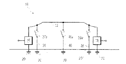
[0023] FIG. 3 is a schematic diagram of another portion of an electrical power
transmission grid utilizing current-diverting paths in accordance with an
aspect of the
invention.
[0024] FIGS. 4A and 48 respectively show schematic diagrams of wye-connected
windings and delta-connected windings with associated current-diverting paths
in
accordance with an aspect of the invention,
[0025] FIG. 5A is a front plan view of a current-diverting path with a self-
supporting
grounded electrode in accordance with an aspect of the invention,
[0026] FIG. 5E3 shows a partial cross-sectional view of an electrically and
horizontally
supporting connection device and associated structure of FIG. 5A.
[0027] FIG. 5C shows a partial cross-sectional view of the electrically and
horizontally
supporting connection device and associated structure of FIG. 58 taken at
arrows 5C,
5C in FIG. 58.
[0028] FIG. 5D shows a cross-sectional view taken at arrows 50, 50 in FIG. 5A.
[0029] FIGS. 6A and 68 show simplified top plan and associated cross-sectional
views
of a high-voltage cold-cathode field emissions triode that may be used in the
present
invention.
[0030] FIGS. 6C and 6D show similar views to FIGS, GA and 68, but for a
bidirectional
high-voltage cold-cathode field-emission electron tube.
[0031] FIG. 6E shows a simplified side plan view, partially in cross section,
of a
bidirectional high-voltage cold-cathode field-emission electron tube.
[0032] FIG. 6F shows a side perspective view of a reentrant tube holder and
ceramic
housing for a switch used in the present invention.
[0033] FIG. 6G is a detail view, partially in cross section, taken at arrows
6G, 6G in FIG.
6F of the electrical and mechanical connection of a high voltage cold cathode
field-
emission tube to the reentrant tube holder of FIG. SF.
[0034] FIG. 7 shows an electrical schematic diagram of a current-diverting
path with
control circuitry for protection against an NEMP or NNEMP in a conductive path
normally at a DC voltage.
CA 02772219 2012-02-24
WO 2011/028300 PCT/US2010/026708
[0035] FIG. 8A shows an electrical schematic diagram of a current-diverting
path with
control circuitry for protection against an NEMP or NNEMP in a conductive path
normally at an AC voltage.
[0036] FIG, 8B shows an electrical schematic diagram of a current-diverting
path with
control circuitry for protection against an NEMP, a NNEMP and a GIC in a
conductive
path normally at an AC voltage.
[0037] FIG. 8C shows a simplified perspective view of a high speed current
shunt with
insulation omitted for purpose of clarity of illustration.
[0038] FIG. 80 shows an enlarged side plan view of a conductive metal strap
and
tapered plates with insulation.
[0039] FIG. BE shows an enlarged perspective view of plates of a transmission
line as
joined to a coaxial cable.
[0040] FIG. 8F shows an enlarged side plan view, partially in cross section,
of electrical
connections and insulation shown in FIG. BE.
[0041] FIG, 8G shows an enlarged top plan view of one of the interconnections
and
associated insulation shown in FIG. BE,
[0042] FIG. 9 shows an electrical circuit diagram of some components of a
power
transmission system and associated current-diverting paths.
[0043] FIG. 10 shows a side plan view of a complete current-detection and
current-
diversion apparatus for a wye-connected electrical component.
[0044] FIG. 11 shows a simplified perspective view of the interconnections of
current-
diverting elements to a delta-connected electrical component.
[0045] FIG. 12 shows a simplified side plan view, partially in cross section,
of a flange-
mounted, bidirectional high-voltage cold-cathode field-emission electron tube.
[0046] PIG. 13 shows a side perspective view of the flange-mounted electron
tube of
FIG. 12.
[0047] FIG, 14 is an enlarged, detail cross-sectional view of an optional
bypass
capacitor taken at arrows 14, 14 in FIG, 13,
6
CA 02772219 2012-02-24
WO 2011/028300
PCT/US2010/026708
DETAILED DESCRIPTION OF THE DRAWINGS
[0048] FIGS. 1A-1C show a typical portion of an electrical power transmission
grid and
illustrate different types of extraordinary electromagnetic pulses (EEMP's)
that may be
received by the grid.
[0049] FIG. IA shows a portion of an AC electrical power transmission grid 10
that
may be protected from an EEMP in accordance with the present invention. Grid
10
includes a power transmission line 12, suspended from transmission towers 14a
and
14b, and may typically be much longer than as illustrated. Electrical
transformers 16
and 18 are respectively situated at the two ends of power transmission line
12. Each
transformer may comprise one phase of a 3-phase wye-connected transformer, by
way
of example. A lower-shown electrode of each transformer 16 and 18 is shown
connected to a respective earth ground 20. As is typical, each earth ground
may
comprise an electrical conductor buried in the ground to assure a more robust
connection to earth ground. In order to assure a more robust ground for
purposes of
increasing the effectiveness of the present invention, it may be desirable to
inject a
conductive agent into the ground, such as a supersaturated solution of Copper
Sulphate,
[0050] FIG, 18 shows grid 10 of FIG. 1, with transmission line 12 receiving an
EEMP
22 of the nuclear electromagnetic pulse (NEMP) or non-nuclear electromagnetic
pulse
(NNEMP) variety. Pulse 22 is shown with associated arrows indicating direction
of
movement of the pulse. After being received by transmission line 12, NEMP or
NNEMP 22 can follow either of two conductive paths 24 or 26 that respectively
include
transformers 16 and 18 and earth ground 20. NEMP or NNEMP 22 may typically
induce current in conductive paths 24 or 26 far in excess of the current-
handling
capability of transformers 16 and 18, and would thereby render inoperative the
transformers unless NEMP or NNEMP 22 is diverted away from them
[0051] FIG. 1C shows grid 10 of FIG, 1, with transmission line 12 receiving an
EEMP
of the geomagnetically-induced current (GIC) variety. Such pulse is shown at
28, with
associated arrows showing direction of movement of the pulse. After being
received
on transmission line 12, GIC pulse 28 can follow either of two conductive
paths 30 or
32 that respectively include earth ground and transformers 16 and 18. GIG
pulse 28
may typically induce current in conductive paths 30 or 32 far in excess of the
current-
7
CA 02772219 2012-02-24
WO 2011/028300
PCT/US2010/026708
handling capability of transformers 16 and 18, and would thereby render
inoperative
the transformers unless GIC pulse 28 is diverted away from them.
[0052] FIG, 2A shows a simplified version of FIG. 1 with various current-
diverting paths
36, 38 and 40. Current-diverting paths 36 and 38 respectfully divert current
away from
transformers 16 and 18. Optional current-diverting path 40 diverts current
from a
portion of transmission line 12, receptive of an EEMP, to prevent such portion
of line 12
from being rendered inoperative by the EEMP. Each of paths 36, 38 and 40
constitutes a low-inductance, high current capacity circuit relative to the
respective,
associated electrical components of grid 10, and is shown diagrammatically as
a switch
37a, 39a or 41a. As such, an EEMP can be diverted from transformers 16 and 18
and
from a portion of transmission line 12, receptive of an EEMP, before the EEMP
can
render such electrical components of the grid inoperative.
[0053] FIG. 28 shows current-diverting path 36 of FIG. 2A in more detail.
Current-
diverting path 36 includes a protective device 37 consisting of a switch 37a
and a
switch controller 37b whose details are described below. It is desired for
length 42,
between an upper node 16a of transformer 16 and path 36, to be as short as is
physically possible, so that the distance 43 between transformer 16 and
current-
diverting path 36 can be minimized. This is important to keep the risetime of
the
current-diverting path 36 fast enough to ensure the diversion circuit path is
completed
before the damaging pulse reaches the protected component. It may
also be
desirable to provide a vacuum capacitor (not shown) in parallel with current-
diverting
path 36, for suppressing ordinary EMP's, such as minor transients. This is
true for the
other current-diverting paths described herein.
[0054] As shown in FIG. 2C, switch 37a may be embodied as a bidirectional high-
voltage cold-cathode field-emission bi-directional electron tube known as a Bi-
tron 44.
The name "81-Von" has been coined by the current inventor as a trademark, and
its
construction is described below. Alternatively, as shown in FIG. 2D, switch
37a may be
embodied as a pair of back-to-back connected high-voltage cold-cathode field
emissions triodes. The bi-directionality of switch 37a (FIG, 28) allows the
switch to turn
on no matter what the polarity of the line voltage on transmission line 12 is
relative to
earth ground 20. This prevents a delay in turning on switch 37a of up to V2
cycle for AC
line voltage on transmission line 12. Bedirectionality of switch 37a is also
desirable so
that the switch conducts an EEMP that passes downwardly through transformer 16
(or
8
CA 02772219 2012-02-24
WO 2011/028300
PCT/US2010/026708
other protected electrical component) as in FIG. 1B, or an EEMP that passes
upwardly
through transformer 16 (or other electrical component) as in FIG, IC.
[0055] In FIG. 2C, the electrodes of Bi-tron 44 comprise first and second
cathanodes
132 and 136, and first and second grids 102 and 110. In FIG. 2D, the
electrodes for
each of high-voltage cold-cathode field emissions triodes 45a and 45b comprise
an
anode 100, a grid 102 and a cathode 104.
[0056] When protecting against NEMP, NNEMP and GIC, either the Bi-tron of FIG.
2C
or the back-to-back high-voltage cold-cathode field emission triodes of FIG,
2D are
equally applicable to DC transmission lines as it is to AC transmission lines.
This is
due to the difference in current flow directions of EMP versus GIC pulses, as
illustrated
in FIGS. 1B and 1C, which requires bidirectional switching means. Both
switches
preferably have risetimes of less than 100 picoseconds, so as to protect
against
NEMP's and NNEMP's. Switches with significantly slower risetimes will not be
effective
in suppressing NEMP's and NNEMP's. Slower risetimes increase the likelihood of
sustaining damage to the protected electrical components,
[0057] In FIGS. 2A and 2B, an appropriate switch 37a for current-diverting
path 36 has
several design requirements: it must turn on before an EEMP can render
inoperative
the protected electrical components, i.e., transformers 16 and 18 in FIG. 2A,
and it also
must handle the high currents typical of EEMPs. FIGS. 2E and 2F respectively
show
typical waveforms for a nuclear electromagnetic pulse (NEMP) and an EEMP
arising
from geomagnetically-induced current. These figures are presented for
considering the
requirements of switches 37a and 39a and similar switches described herein for
diverting EEMP's around electrical components to be protected from such
pulses.
[0058] FIG, 2E shows a NEMP 46 and further shows sequential stages 46a, 46b
and
46c of such NEMP. During stage 46a, for example, an NEMP 46 rises to well
above 20
volts per meter in field strength in less than 100 picoseconds. Pulses of this
fast a
risetime and with amplitudes equal to or greater than 20 volts per meter,
whether
NEMP or NNEMP, should be protected against, It is necessary to use a switching
means with a risetime faster than 100 Picoseconds to prevent an electrical
component
from becoming inoperative due to NEMP 46 or an NNEMP (not shown). An
acceptable
risetime 47 is about 80 picoseconds. Risetimes significantly longer than 100
9
CA 02772219 2012-02-24
WO 2011/028300
PCT/US2010/026708
picoseconds are likely to allow damage to components sought to be protected.
The
likelihood increases as the risetime increases.
[0059] The NEMP waveform 46 shown in FIG. 2E is a representative member of the
class of waveforms commonly known as EMP, and more specifically as NEMP and
NNEMP. These waveforms are each unique, but collectively share important
common
characteristics such as fast risetime. it is important to recognize that NEMP
and
NNEMP share common characteristics (e.g., risetime) and, from the point of
view of the
current invention and the protected electrical components, are
indistinguishable.
(0060] FIG. 2F shows a current-versus-time waveform for an EEMP 48 arising
from a
GIC pulse, and is an actual recording of a GIC that occurred January 13, 1999
in
Finland, From FIG. 2F, it can be seen that either waveform is capable of
inducing
potentially damaging transients in an electrical power system,
[0061] FIG. 3 illustrates protected electrical components having inputs or
outputs
floating with respect to earth ground as is found in delta-connected 3-phase
circuits, for
example. Thus, FIG. 3 snows an electrical generator 50 with a AC output
appearing on
output lines 50a and 50b, and a transformer 52 having its left-shown winding
connected to lines 50a and 50b and having its output winding connected to
output lines
52a and 52b. Lines 50a, Sob, 52a and 52b are all floating with respect to
earth ground
20. Transformer 52 may comprise one phase of a 3-phase delta-connected
winding,
by way of example.
[0062] In FIG. 3, current-diverting path 54 protects generator 50, while
current-diverting
path 56 protects the left-shown primary winding of transformer 52. Optionally,
current-
diverting path 58 can provide a path for dissipation of current in line 50b
through earth
ground 20. The mentioned current-diverting paths conform to the above
description of
current-diverting paths: such as path 36 in FIG. 28. Path 58 is especially
desirable as
it allows the circulating energy created by the two current-diverting paths to
dissipate to
ground.
[0063] FIG. 4A shows one side 60 of wye-connected transformer windings 60a,
60b
and 60c. Each winding 60a, 60b and 60c is shunted by an associated current-
diverting
path 62, 64 or 66, in accordance with an aspect of the invention. Paths 62, 64
and 66
are each shown in simplified form as a bi-directional switch of Bi-tron
configuration,
although control circuitry described below would be used to operate the Bi-
tron
CA 02772219 2012-02-24
WO 2011/028300
PCT/US2010/026708
switches. In this wye-connected side 60 of a transformer, one end of each of
the
windings and associated current-diverting paths is connected to earth ground
20.
[0064] FIG, 46 shows one side 68 of delta-connected transformer windings 68a,
68b
and 68c. Each winding 68a, 68b and 68c is shunted by an associated current-
diverting
path 70, 72 or 74 in accordance with an aspect of the invention. Paths 70, 72
and 74
are each shown in simplified form as a bi-directional switch of Bi-tron
configuration,
although control circuitry described below would be used to operate the Bi-
tron
switches. In this delta-connected side 68 of a transformer, neither end of the
windings
or of their associated current-diverting paths is connected to earth ground
(not shown).
[0065] FIGS. 5A and 5B illustrate a current-diverting path 78 that may be used
in the
case of wye-connected windings, as for instance, to implement in FIG. 4A
current-
diverting path 62, 64 or 66. As with paths 62, 64 and 66, current-diverting
path 78 of
FIG, 5A is connected to earth ground 20,
(0066] In FIG. 5A, current-diverting path 78 includes an electrically-
insulated and
vertically-supporting ground conductor 80, a vacuum housing 81, and an
electrical and
horizontally-supporting connection device 83 to a conductor 84 of an
electrical power
transmission grid. As further detailed below, vacuum housing 81 preferably
contains a
switch, such as shown schematically in FIG. 28 at 37a, together with circuitry
for
detecting EEMP's. Insulated ground conductor 80 is preferably vertically
self-
supporting, with its lower end mechanically affixed to a mechanical support
88, shown
diagrammatically.
[0067) FIGS. 56 and 5C show more details of a preferred construction of
electrical and
horizontally-supporting connection device 83 of FIG. SA, which minimizes the
conductive path length from conductor 84 to EEMP detection circuitry within
vacuum
housing 81. This, in turn, decreases the risetime of the switch within housing
81.
[0068] Housing 81 preferably comprises dielectric material that is optionally
covered
with a KEVLAR or similar aramid-fiber jacket 82 to make housing 81 more
resistant to
environmental hazards, such as sandstorms or being shot with a bullet. The
connection
to the power conductor 84 is made by a metal connector assembly 86, with metal
connecting part 86e vacuum sealed to housing 81 at locations 86a, for
instance. Metal
connector assembly 86 includes clamps 86b, 86c and 86d for clamping onto
conductor
84, which fits within a generally V-shaped groove 86f, wherein any sharp edges
have
11
CA 02772219 2012-02-24
WO 2011/0283011 PCT/US2010/026708
been removed. Clamps 86b, 86c and 86d may be held onto metal connecting part
86e
with appropriate screws 86g, for instance,
(0069] FIG, 50 is a cross-sectional view of insulated ground conductor 80
taken at
arrows 50, 50 in FIG, 5A. Insulated ground conductor 80 has an inner part 80a
and
outer part 80b. Inner part 80a preferably comprises an elongated, conductive
stainless
steel core 90, encircled by a conformal conductive chrome sheathing layer 92,
which in
turn is covered by a conformal conductive copper sheathing layer 94.
Sheathings 92
and 94 are preferably applied by the plasma-spray process. Alternatively,
sheathings
92 and 94 could be applied as thick electroplated layers. Preferably, a
corrosion-
resistant dielectric protective layer 96 covers copper sheathing layer 94.
Protective
layer 96 is preferably applied by electrostatic powder coating. A KEVLARt or
similar
aramid-fiber jacket 99 preferably encases outer part 80b to provide resistance
against
environmental hazards, such as sandstorms or being shot with a bullet.
[0070] In order to handle high currents when conducting EEMPs, chrome
sheathing
layer 92 should intimately conform to stainless steel core 90, and copper
sheathing
layer 94 should intimately conform to chrome sheathing layer 92. Additionally,
for low
inductance, stainless steel core 90 preferably should have a vertical-to-
horizontal
dimension in FIG, 50 exceeding 10:1, and the edges 98a, 98b, 98c and 98d of
inner
part 80a of insulated ground conductor 80 are preferably radiused such that
the radius
equals approximately half the vertically shown dimension of core 90 and layers
92 and
94.
[0071] Outer part 80b of insulated ground conductor 80 preferably comprises
ceramic
or terra cotta or other dielectric material having resistance to high
temperatures. This is
necessary due to high current level through conductor 80 which can, in some
extreme
cases, cause said ground conductor 80 to heat up due to 12R heating.
[0072] FIGS. 6A and 6B show basic structure of the high-voltage cold-cathode
field
emission triode 45a or 45b) of FIG. 20, also known as a Pulsatron as described
in
USP 4,950,962 by the current inventor and others. However, the Pulsatron is
scaled in
size to operate in the continuous mode at a desired voltage. Triode 45a
includes a
cylindrically shaped cathode 100 which is encircled by a cylindrically shaped
grid 102,
which in turn is encircled by a cylindrically shaped anode 104. Grid 102 is
shown as
dashed lines to indicate that it would have suitable holes for passage
therethrough of
12
CA 02772219 2012-02-24
WO 2011/028300 PCT/US2010/026708
electrons. The anode 104, grid 102 and cathode 100 share a common main axis
(not
shown). The radial spacing from cathode 100 to grid 102 is such as to create
therebetween a circular waveguide supporting the transverse electromagnetic
mode
(TEM). In FIGS, 6A and 6B, the cathode 100 is comprised of a graphite
material, the
grid 102 is comprised of a conductive metal such as stainless steel, and the
anode 104
is comprised of a refractory metal such as tungsten, by way of example.
(0073] FIGS. 6C and 60 shows basic structure of the high-voltage cold-cathode
field
emission tube 44 of FIG. 2C, also known as a Bi-tron as mentioned above. Bi-
tron 44
includes a cylindrically shaped electrode 106, referred to herein as a
cathanode; that is,
an electrode that can function as either a cathode or an anode. Encircling
cathanode
106 (referred to as first cathanode 132 in FIG. 2C) is a cylindrically shaped
first grid
102, which in turn is encircled by a cylindrically shaped second grid 110,
which is then
encircled by a cylindrically shaped cathanode 112 (referred to as a second
cathanode
136 in FIG. 2C). First and second grids 102 and 110 are shown as dashed lines
to
indicate that they would have suitable holes for passage therethrough of
electrons.
The cathanocies 106 and 112, and the first and second grids 102 and 110 share
a
common main axis (not shown). The radial spacfing from cathanode 106 to grid
102 is
such as to create therebetween a circular waveguide supporting the transverse
electromagnetic mode (TEM). Similarly, the radial spacing from cathanode 112
to grid
110 is such as to create therebetween a circular waveguide supporting the
transverse
electromagnetic mode (TEM). The radial spacing between the first grid 102 and
the
second grid 110 is sufficient to prevent flashover therebetween at an intended
operating voltage. In FIGS. 6C and 60, the cathanodes 106 and 112 are
comprised of
a graphite material and the grids 102 and 110 are comprised of a conductive
metal
such as stainless steel, by way of example.
[0074] Both the triode 45a of FIGS. 6A and 6B and the Bi-tron 44 of FIGS. 6C
and 6D
beneficially can handle current levels of 400 Amps per square centimeter. The
speed
of each of these switches is preferably enhanced by so-called top-hat sockets
described below.
[0075] There are several critical conditions that must be met when designing a
grid for
a cold cathode field-emission electron tube, a Bi-tron or a Pulsatron. They
are:
13
CA 02772219 2012-02-24
WO 2011/0283011 PCT/US2010/026708
1. The grid-cathode or grid-cathanode spacing must be constant across the
length of the grid. This is usually accomplished by placing the grid under
high
tension or building it with a rigid structure.
2. The number of elements in the grid must be high enough to ensure a
constant and uniform electric field in the grid-cathode or grid-cathanode
region.
3. There must be no sharp edges of burrs anywhere in the grid structure.
Rather, individual elements can be round, flat or high aspect-ratio elliptical
shapes. All edges must be fully radiused. In this context, fully racliused
means
that the edge in question has a radius equal to half the thickness of the
material.
[0076] The actual implementation of these design rules is determined by the
size of the
grid being built.
[0077] FIG. 6E shows a Bi-tron 162, which is a form of bidirectional high-
voltage cold-
cathode field-emission electron tube. Tube 162 includes an electrically-
insulated
housing 116, first and second cathanodes 132 and 136 (referred to as 106 and
112 in
FIG. 6C) mounted on respective first and second cathanode connectors 134 and
138.
First and second grids 102 and 110 are mounted on respective grid feedthroughs
126a
and 126b. A chemical getter pump 118 is mounted on getter pump feedthrough 120
and is used to maintain the vacuum in the housing 116 during periods when no
electric
power is available. A vacuum exhaust tipoff 122 is created at the end of the
manufacturing cycle and is used to seal off the housing 116 from the
manufacturing
equipment. The electron tube 168 shown in FIGS. GA, 6B, and the electron tube
162
shown in FIGS. 6C, 6D, are designed for a substantially higher operating
voltage, and
hence have a different aspect ratio, than the electron tube shown in FIG. 6E.
[0078] FIG. 6F shows a reentrant tube socket 142. which lowers the inductance
of
connections to a Bi-tron 162 or a Pulsatron 168 electron tube and reduces
risetime of
the switch by a factor that may typically be 6:1. This tube socket 142 is
primarily
designed for use with parallel plate transmission lines, although it can be
successfully
integrated into other circuit configurations. Reentrant tube socket 142
comprises
preferably identical conductive top-hat shaped members 144 and 146 that
respectively
enclose the two longitudinal ends of the electrically-insulated housing 116
shown in
FIG. 6E. Each conductive top-hat shaped member 144 and 146 has a respective
rim
144a or 146a for connecting to external circuitry. Electrical connection from
circuitry
14
CA 02772219 2012-02-24
WO 2011/028300 PCT/US2010/026708
within electrically-insulated housing 116 to members 144 and 146 may be
accomplished as shown in FIG. 6G. As that figure illustrates, conductive tab
150 of
member 144 interconnects with the cathanode connector 138 by means of a
mounting
screw 151, Conductive tab 150 is connected to the first or second cathanode
connector 134 or 138. The combination of the conductive mounting tab 150 and
mounting screw 151 also provide a mechanical interconnection between top hat
shaped member 144 or 146 and the electron tube 162 or 168. The conductive
mounting tab 150 is preferably welded to the top of the conductive top-hat
shaped
members 144 and 146. It will be apparent to those skilled in the art that
various
clearance holes (e.g., 147) and slots (e.g., 149) in the top-hat shaped
members 144
and 146 are required to accommodate electrical connections such as grid
feedthrough
126 on electron tubes 162 or 168.
[0079] Rims 144a and 146a are spaced apart from each other to prevent
flashover
between them. If desired, an additional insulator 212 (FIG. 10) described
below can be
pieced between the rims, which further lowers the inductance of connections to
the
switch, thus further decreasing risetime of the switch,
[0080] By placing the entire Bi-tron tube 162 of FIG, 6E inside a shielded
housing and
making various geometrical changes, it is possible to eliminate the need for
the
reentrant tube socket 142 of FIG. 6F. Such an arrangement is described below
in
connection with FIGS. 12-13.
[0081] FIG. 7 shows a DC threshold detector circuit 152, which implements a
current-
diverting path 154 with a control circuit for protecting against an NEMP or
NNEMP in a
conductive path normally at a DC voltage. Path 154 includes a unidirectional
switch,
comprising a high-voltage cold-cathode field emission triode 168, known as a
Pulsatron
tube and associated control circuitry. Tube 168 is biased to a standoff
condition (i.e.,
not conducting) at normal line voltage plus an acceptable excess voltage. When
the
excess voltage value is exceeded, the threshold detector circuit 152 causes
the tube
168 to go into conduction so as to create current-diverting path 154.
[0082] In particular, in FIG, 7, the tube 168 is biased to shut-off by the
network
composed of resistors R1 and R2, which form a voltage divider. Resistors R1
and R2
establish a grid voltage that is proportional to the voltage on line. The tube
is oriented
appropriately to the polarity of the transmission line to which it is
attached. The
CA 02772219 2012-02-24
WO 2011/028300 PCT/US2010/026708
schematic shown is for a negative polarity line. The resistor R1 is a
relatively low value
resistor and resistor R2 is a relatively high value resistor. This places the
grid close to
the cathode potential. This relationship is maintained in all Pulsatron and Bi-
tron
circuits described below in connection with FIGS. 8A-8B: in regard to these
figures, the
resistors with an odd reference numeral (i.e., 1, 3 and 5) have lower values
relative to
their associated resistor in a voltage-divider network with an even reference
numeral
(i.e.. 2, 4 and 6). Further, the resistors with an odd reference numeral
preferably are
adjustable resistors, as diagrammatically shown. The specific values are
dependent on
the voltage at which the circuit operates. The capacitor C1 is used to
maintain the
control voltage if the line voltage goes low for a short period. This is also
true for
capacitors C2 and C3 in FIGS. 8A-8B.
[0083] Referring to FIG. 7, if the voltage on line 158 rises beyond a
threshold level, the
balance established by the voltage divider R1-R2 network is upset and the tube
168
starts conducting. The threshold level is chosen so that the presence of an
NEMP or
NNEMP in a conductive path (not shown) including a protected electrical
component is
detected prior to the pulse reaching and rendering inoperative such electrical
component. Accordingly, current-diverting path 154 with tube 168 diverts the
NEMP or
NNEMP around the protected electrical component with a low inductance, high
current
capacity circuit relative to the electrical component, before the pulse can
reach and
render the electrical component inoperative.
[0084] FIG. 8A shows a current-diverting path 160 with control circuitry for
protection
against an NEMP or NNEMP in a conductive path normally at an AC voltage.
However,
to allow operation in an AC circuit, a bidirectional Bi-tron 162 is used
rather than the
unidirectional Pulsatron tube 168 of FIG. 7. To accommodate the bi-directional
aspect
of the circuit, a second voltage divider R3-R4 and capacitor C2 are included.
The
operation of the detection of NEMP or NNEMP and diverting current away from a
protected component as described in connection with FIG. 7 apply to FIG. 8A,
except
for the duplication of the control network to accommodate AC operation.
[0085] FIG. 8A also shows a high-speed current shunt 164 in the ground leg of
the
circuit. This shunt provides an output when the Bi-tron 162 conducts, This
output on
node 166 can be used to advise system operators of an EEMP event, or as a
means of
triggering other protective circuitry.
16
CA 02772219 2012-02-24
WO 2011/028300
PCT/US2010/026708
[0086] FIG. 86 shows a preferred control circuit 167. Circuit 167 is similar
to FIG, BA,
but shows a GIG detection circuit 169 for detecting a GIG, The GIC detection
circuit
169 comprises voltage-divider network R5-R6 and capacitor C3, together with a
Pulsatron 168, When a GIG causes current flow upwardly through the ground
path, the
current traversing current shunt 164 develops a voltage proportional to the
magnitude
of the current and its temporal waveform. Such voltage triggers Pulsatron 168
into
conduction.
[0087] Sequentially turning on Pulsation 168 and then 81-tron 162 takes longer
than
the Elv1P sensing processes of FIGS. 7 and 8A, so that speed is not as
critical due to
the slower risetimes of GC's which are detected with the control circuitry for
Pulsatron
168. As with capacitors Cl of FIG. 7 or Cl and C2 of FIG. 8A, capacitor C3
performs a
"Keep-alive' function.
[0088] Current shunt 164 of FIGS. 8A and 88 is now described in connection
with
FIGS. 8C-8G. FIG. 8C shows high speed current shunt 164, which is comprised of
a
flat conductive metal strap 170, with connection holes 170a for connection to
a ground
path of an external circuit, Metal strap 170 is preferably made of copper or
having
conductivity at least as low as commercial grade copper. "Commercial grade"
connotes copper refined to at least 94 percent copper by mass. Copper strap
170
preferably has fully radiused ends 1701), with holes 170a for respective
connections to
node 172, also shown in FIGS. 8A and 88, and earth ground 20. Holes 170a are
provided for electrical connection purposes. Preferably, the edges of copper
strap 170
are cleburred and radiused. Current shunt 164 has the ability to measure pulse
currents in excess of 100,000's of Amps.
[0089] FIG. 8C also shows a tapered parallel-plate transmission-line matching
transformer 174 being preferably silver-soldered to copper strap 170 at the
dual ends
of a defined current measuring region 171. The narrow ends of plates 174a and
174b
in transmission line 174 are preferably silver-soldered to an end 173 of a 50-
ohm
coaxial cable 176. Coaxial cable 176 must be at least about i4inch (12.77 mm)
in
diameter to handle the high voltage that results from large amounts of current
across
the measuring region 171. Increasing amounts of currents force the use of
progressively larger diameter coaxial cable to handle the increased voltage
produced
by the measuring region 171 of the shunt 164. The width of each of plates 174a
and
174b at their connection junctures to metal strap 170 is preferably
approximately the
17
CA 02772219 2012-02-24
WO 2011/028300 PCT/US2010/026708
same, although these widths may vary from about 0.9 to 1.1 times the width of
the
strap 170.
(0090] The ratio of the length of upper plate 174a to the width of the flat
metal strap
170 preferably is approximately 10 to 1. Lower ratios lead to increasing
impedance
mismatch. Having a ratio substantially larger than 10 to 1 leads to an overly
large and
ungainly structure. Further, plates 174a and 174b can have various tapers from
their
narrow ends to their wide ends. For example, the simplest taper is a straight
line so
that the plates approximate equilateral triangles. A preferred taper is more
complex so
as to have exponentially varying sides to the foregoing equilateral triangle,
approximating the curve of the bell (or output orifice) of a musical trombone.
(00911 FIG, 8D shows a side view of copper strap 170, upper and lower plates
174a
and 174b of transmission line 174, and insulation 178a and 178b. Such
insulation
178a and 178b are omitted from FIG. 8C for clarity of illustration. Insulation
178a
extends the entire length under first plate 174a, from the juncture of the
copper strap
170 and the wide end of upper plate 174a to an end in slot 188 in the center
insulation
177 (FIG. 8E) of a coaxial cable 176. Slot 188 (FIG. 8E) serves the function
of
eliminating a line-of-sight path for electrons to prevent a short circuit from
forming
between center conductor 182 and coaxial shield 186. Insulation 178b
preferably
extends a minimum of one-half the length of lower plate 174b under such plate
from
the juncture of the copper strap 170 and the wide end of lower plate 174b.
[0092] FIG. 8E shows the tapered parallel-plate transmission line 174
connected to
coaxial cable 176. As shown in that figure, the center conductor 182 of the
coaxial
cable 176 is soldered (as shown by a solid black region) to the upper side of
the upper
plate 174a. Similarly. coaxial cable shield 186, shown with an enlarged view
of braids
of wires forming the shield, is soldered (as shown by a solid black region) to
the
underside of lower plate 174b. Preferably, the foregoing solder connections
are made
using silver solder with a silver content exceeding approximately 5 percent by
mass.
(0093] FIG, 8F shows transmission line 174 with upper plate 174a preferably
silver-
soldered to center conductor 182 and lower plate 174b preferably silver-
soldered to
shield 186 of coaxial cable 176. As mentioned above, insulation 178a is
inserted into
slot 188 in center insulation 177 of cable 176_
18
CA 02772219 2012-02-24
WO 2011/028300
PCT/US2010/026708
[0094] FIG. 8G shows first plate 174a silver-soldered to center conductor 182
in cable
176, Insulation 178a can be seen protruding from under first plate 174a,
[0095] The foregoing current shunt 164 of FIGS. BC-8G can be arranged with the
upper and lower plates 174a and 174h functionally interchanged, To visualize
this, in
the foregoing discussion, the upper plate 174a was the 'hot" conductor and the
lower
plate 174b was the 'ground" conductor, In the alternative version, these
functions are
interchanged so that the upper plate becomes the ground conductor and is
attached to
the shield 186 of coaxial cable 176, and the lower plate becomes the hot
conductor and
is attached to the center conductor 182 of coaxial cable 176. In this
configuration, the
insulation 178b is now inserted into slot 188 of coaxial cable 176,
[0096] As is well known in the art, high frequency electricity travels at the
skin of a
conductor in a process known as the skin effect. The skin effect cannot be
ignored in
direct measurements of high-speed pulse currents, and a mathematical
compensation
is required to extract an exact measurement of the current. A current shunt
converts
current into voltage as a function of voltage drop across a current-measuring
region.
Attention must be paid to proper impedance matching of the current-measuring
region
to the measuring instrument, The foregoing concern is addressed by the
incorporation
of the above-described tapered parallel-plate transmission-line matching
transformer,
[0097] The current shunt output must be corrected for high frequency operation
due to
the skin effect on resistance. The formula for skin depth correction (and
therefore
impedance as a function of frequency) of a rectangular cross-section shunt is
well
known and, as applied to the present current shunt, is as follows:
ith 111: f P
2(w + t)
where:
= impedance of current-measuring region 171
Ith = length of current-measuring region 171
w = width of conductive strap 170
= thickness of conductive strap 170
f = frequency (risetime)
p = permeability (Him) of conductive strap 171
a = conductivity (1/0-m) of conductive strap 171
19
CA 02772219 2012-02-24
WO 2011/028300
PCT/US2010/026708
Note: For a copper shunt operating in air, the permeability is taken as 1.
[0098] Ohm's Law is applied (Voltage/Resistance Current
using the Z value for
Resistance) to determine the current. It is, of course, necessary to convert
risetime to
frequency by the established method.
[0099] FIG. 9 shows a pair of protected electrical components 190 and 192 with
associated current-diverting paths 194 and 196 including protective devices
194a and
196a and preferably a pair of normally-closed series switches 198a and 198b.
Components 190 and 192 may be windings of a transformer or an electrical
generator,
by way of example. The protective devices 194a and 196a in current-diverting
paths
194 and 196 are examples of protective device 37 of FIG. 2B. Normally-open
switches
in protective devices 194a and 196a close upon detection of an EEMP event NEMP
and NNEMP events are detected as voltages preferably by control circuit 167a
and
167b (see 167 in FIG. BB), and GIG events are detected as currents by current
shunts
164a and 164b operating in conjunction with control circuits 167a and 167b as
shown
in FIG, 9.
[00100] Upon
receipt of suitable voltage or current inputs, control circuit 167a
outputs a control signal to activate normally-closed switch 198a. Similarly,
upon receipt
of suitable voltage or current inputs, control circuit 167b outputs a control
signal to
activate normally-closed switch 198b. The closing of the normally-open
switches in
response to control signals from control circuits 167a and 167b cause devices
194a
and 196a to collapse the magnetic field in windings 190 and 192, and create
current-
diverting paths 194 and 196, respectively. The switches in the protective
devices 194a
and 196a also produce an output that is used to trigger the opening of
normally-closed
switches 198a and 198b after a predetermined time after detection of an EEMP
of no
more than two cycles of the line voltage. This is for the purpose of removing
a short
circuit from protected component 190. Arrows 200 show the circulating path of
current
produced by the EEMP event in the current-diverting paths 194 and 196. The
direction
the foregoing current depends on instantaneous polarity of the circuit at the
time of the
EEMP event, and may or may be in the direction of the arrowheads as shown. The
normally-closed switches 198a and 198b of FIG. 9 may be any type of switch
with
suitable voltage, current, and response-time ratings. which would include a Bi-
tron 44
or 162 (FIG. 2C or FIG. 6E),
CA 02772219 2012-02-24
WO 2011/028300
PCT/US2010/026708
[00101] FIG. 10 shows a complete EEMP protection device 204, which is
the
preferred embodiment of the FIG. 8B electrical schematic for wye-connected
electrical
components. The device 204 has two types of internal vacuum pumps. One ts a
chemical getter pump 118. This is always functional. The second is an ion pump
206
of conventional design but of open construction for maximum conductivity.
There is an
internal magnetic shielding 208 to preclude interference with the electron
trajectories in
the adjacent switch tube 162 of FIG. 10 or switch tube 168 (not shown). While
the ion
pump 206 requires a small amount of electricity to operate, it is critical to
ensure that
the vacuum is properly maintained at all times in the enclosure. The chemical
getter
pump 118 maintains the vacuum when electricity is not available, such as
during
shipping, installation, maintenance or blackouts,
[00102] Contained within vacuum housing 81 is the switch tube 162 or
168
mounted inside the reentrant tube socket 142, Top-hat shaped sockets 144 and
146
are separated by an insulator wall 212. This wall 212 serves the dual purpose
of
providing additional electrical insulation between the two sockets 144 and 146
and
simultaneously provides a mechanical mounting means for the tube 162 or 168
and
reentrant tube socket 142. The preferred control circuit 167 is connected to
the
electrodes of tubes 162 and 168. One of the electrical connection leads, 210a,
runs
through an insulated feedthrough tube 210 to allow an insulated electrical
connection to
electrodes of switch tube 162 or 168 on the other side of insulated wall 212.
[00103] With regard to the switch tube 162 or 168, one embodiment
includes the
concept of not having such tubes 162 or 168 in individual vacuum housings,
such as
housing 116 (FIG. 6E). Instead, the tubes are constructed in open housings and
use
the vacuum system 206 instead to maintain the vacuum necessary for their
operation.
[00104] The insulated ground conductor 80 previously described in FIG,
50 has
one end terminated inside the housing 81. The ground conductor 80 may serve
two
functions: when used with an electrical component with windings in a wye
configuration, it provides mechanical support for the EEMP protection device
204 by
supporting the entire weight of said system, and it simultaneously provides a
low-
inductance path to ground 20 to allow completion of the current-diverting path
during
operation. The ground connection means is connected to the balance of the
circuitry
via the current shunt 164 (FIGS. 8C-8G).
21
CA 02772219 2012-02-24
WO 2011/028300
PCT/US2010/026708
[00105] There are two methods of connecting the EEMP protection device
204
for use. They relate to the following two standard wiring schemes for three-
phase
circuitry: wye 60 of FIG. 4A and delta 68 of FIG. 48. These figures show the
respective wiring methods and have been previously described. FIG. 11 shows
one
set of connections of a delta-configured transformer 220. The terminations for
the
windings of the transformer 220 are presented as bushings 222a, 222b, and
222c.
Three EEMP protection devices 204 are positioned side by side and are wired to
place
each device 204 between a respective pair of temiinals constituting a single
phase of
the transformer 220 winding. Thus, device 204a is connected to bushings 222a
and
222b, device 204b is connected to bushings 222b and 222c, and device 204c is
connected to bushings 222c and 222a as shown in FIG.11. This corresponds to
the
transformer winding configuration 68 of FIG. 48.
1001061 For protection of a power system, it is necessary to protect
the primary
and secondary of every transformer of that system with an EMP protective
device 204
installed physically adjacent to the transformer on each phase connection. It
is further
necessary to similarly protect generators of the power system with EMP
protective
devices on each phase connection installed physically adjacent to the
generator itself.
For economic or other reasons, EMP protective devices may be used with fewer
than
all transformers and generators of a power system.
[00107] As an alternative to the Bi-tron tube 162 of FIGS. 6E and 6F,
FIG. 12
shows a Bi-tron tube 225, contained within vacuum-sealed conductive housing
236
having sections 236a and 236b. Housing sections 236a and 236b are continuously
tungsten-inert gas (TIC) welded to a conductive flange 234 by weld beads 237.
The
flange 234 can be mounted to the exterior, conductive wall of a shielded room
or
building, by way of example.
[00108] In FIG. 12, a common conductive element generally marked as 232
passes entirely through the tube 225, passing through primary electrical
insulators
230a and 230b. At 232a the central conductive element 232 is connected the
incoming
power line (not shown) and is referred to hereinafter as line'. Similarly, at
232b the
central conductive element 232 is connected the protected component (not
shown) and
is referred to hereinafter as "load'. Element 232 supports the first cathanode
106 on its
exterior surface. Element 232 preferably has a conductivity at least as high
as that of
Type 304 stainless steel. Various internal electrical insulators (not shown)
are provided
22
CA 02772219 2012-02-24
WO 2011/028300
PCT/US2010/026708
as required, as will be apparent to persons of ordinary skill in the art based
on the
present specification. For instance, the internal connections to the grids 102
and 110.
respectively associated with feedthroughs 126a and 126b, are provided with
preferably
contiguous electrical insulation (not shown) over their entire lengths. FIG.
13 shows an
exemplary perspective view of the Bi-tron tube 225 of FIG. 12.
(001091 Bi-tron 162 of FIGS, 6E and 6F is primarily intended for use
with primary
power grid components such as generators and substation transformers, In
contrast,
Bi-tron 225 of FIGS. 12 and 13 is primarily intended for use as a shielded
feedthrough
and an RF- and EMP-diverting component for use with EMP shielded rooms and
buildings. The flange 234 mount provides a convenient and easily implemented
technique for achieving a fully symmetrically ground connection to an
electrically
shielded wall. Thus, installation of Bi-tron 225 involves no special skills,
merely
requiring the skills of a journeyman electrician for installation,
[00110] The mounting flange 234 has two bolt circles; the outer bolt
circle of
holes 234a is used for physically mounting and installing the Bi-tron 225. The
inner
circle of holes 234b is inside the vacuum enclosure 236a, 236b and provides
vent
holes between the respective housing sections 236a and 236b on either side of
the
flange 234. The flange 234 also contains a threaded boss 238 to which the
outer
cathanocle 112 is mounted.
[00111] As shown in FIGS. 12 and 14, a low pass filter comprising at
least a
bypass capacitor 240 may be advantageously incorporated into Bi-tron 225 for
reducing minor RF transient signals that are below the turn-on threshold of Bi-
tron 225.
Additional or alternative RF filtering components may be incorporated in the
vicinity of
the illustrated location of the bypass capacitor 240.
[001121 One plate 232c of the bypass capacitor 240 may be formed by
enlarging
conductive element 232, as shown. A second plate 242 of the capacitor 240 may
comprise a conductive tubular electrode, which is mechanically suspended from,
and
electrically connected to, either the housing section 236b as shown, or from
the
housing section 236a or both housing sections 236a and 236b. as shown best in
FIG.
14. Second plate 242 of the capacitor 240 may be mechanically suspended from,
and
electrically connected to, the housing section 236b by a support structure
such as
23
CA 02772219 2012-11-28
spokes 244. The spokes 244 are welded to the housing section 236b and may
integrally
formed with the second plate 242.
[00113] It is noted that the Bi-tron control circuitry, as exemplified by
FIG. 8A,
contains a number of discrete electrical components (e.g., R1, R2, Cl, C2
etc.). While it
is preferable that these components be mounted externally to the vacuum
enclosure of
Bi-tron 162 (e.g., FIG. 6E) or of Bi-tron 225 (e.g., FIG. 12), it is possible
to physically locate
some or all of these components inside the vacuum enclosure 236 of FIG. 12 or
116 of FIG.
6E..
[00114] While the invention has been described with respect to specific
embodiments
by way of illustration, many modifications and changes will occur to those
skilled in the art,
all without departing from the scope of the invention, as defined by the
appended claims.
24