Note: Descriptions are shown in the official language in which they were submitted.
CA 02772367 2012-03-23
COMPACT PLANAR INVERTED F-ANTENNA FOR MULTIBAND COMMUNICATION
FIELD OF THE INVENTION
The present invention relates to wireless communication antennas, and more
particularly to a
multiband antenna for wireless communication devices.
BACKGROUND OF THE INVENTION
Wireless communication devices typically use multiband antennas to transmit
and receive
wireless signals in multiple wireless communication frequency bands such as
GSM900/1800,
ISM bands, GPS, and IMT satellite communication. Because of its compact size
and multiband
performance, a Planar Inverted F-Antenna (PIFA) is preferred for multiband
antenna for wireless
communication devices.
Unfortunately, PIFAs exhibit problems related to the radiating branches which
not only generate
lower resonant modes used for the signal transmission/reception but also a
plurality of higher
order resonant modes. These unwanted higher order resonant modes are difficult
to control and
substantially impede the tuning of the multiband antenna.
Furthermore, the radiation caused by the higher order resonant modes
substantially affects the
performance of the low-noise amplifier in the receiver and can even pose the
risk of saturating
the same, as well as severely degrades the performance of the power amplifier.
It is desirable to provide a multiband antenna for wireless communication
devices that is capable
of sending/receiving wireless communication signals in a plurality of
frequency bands.
It is also desirable to provide a multiband antenna for wireless communication
devices that has
substantially reduced radiation associated with unwanted higher order resonant
modes.
It is also desirable to provide a multiband antenna for wireless communication
devices that is
Page 1 of 11
CA 02772367 2012-03-23
compact and simple to implement.
SUMMARY OF THE INVENTION
Accordingly, one object of the present invention is to provide a multiband
antenna for wireless
communication devices that is capable of sending/receiving wireless
communication signals in a
plurality of frequency bands.
Another object of the present invention is to provide a multiband antenna for
wireless
communication devices that has substantially reduced radiation associated with
unwanted higher
order resonant modes.
Another object of the present invention is to provide a multiband antenna for
wireless
communication devices that is compact and simple to implement.
According to one aspect of the present invention, there is provided a multi-
band antenna for
sending/receiving wireless communication signals in a plurality of frequency
bands. The multi-
band antenna has a feed element for sending/receiving signals associated with
the wireless
communication signals. A stepped-impedance structure is connected to the feed
element. The
stepped-impedance structure has a plurality of concatenated stepped-impedance
elements with
each stepped-impedance element having a predetermined impedance and a
predetermined
electrical length associated with a resonance mode for sending/receiving
wireless communication
signals in a respective frequency band of the plurality of frequency bands.
According to the aspect of the present invention, there is provided a multi-
band antenna for
sending/receiving wireless communication signals in a plurality of frequency
bands. An
interdigitated coupled feed element for transmitting signals associated with
the wireless
communication signals is disposed on a dielectric substrate. A stepped-
impedance structure is
disposed on the dielectric substrate and connected to the feed element. The
stepped-impedance
structure has a plurality of concatenated folded stripe lines with each folded
stripe line having a
predetermined impedance and a predetermined electrical length associated with
a resonance
Page 2 of 11
CA 02772367 2012-03-23
mode for sending/receiving wireless communication signals in a respective
frequency band of the
plurality of frequency bands. A shorted element is disposed on the dielectric
substrate with the
shorted element being connected to one of the folded stripe lines at a first
end and connected to a
ground plane at a second end.
The advantage of the present invention is that it provides a multiband antenna
for wireless
communication devices that is capable of sending/receiving wireless
communication signals in a
plurality of frequency bands.
A further advantage of the present invention is that it provides a multiband
antenna for wireless
communication devices that has substantially reduced radiation associated with
unwanted higher
order resonant modes.
A further advantage of the present invention is that it provides a multiband
antenna for wireless
communication devices that is compact and simple to implement.
BRIEF DESCRIPTION OF THE DRAWINGS
A preferred embodiment of the present invention is described below with
reference to the
accompanying drawings, in which:
Figures la and lb are simplified block diagrams illustrating a perspective top
view and a
detailed top view, respectively, of a multi-band antenna according to a
preferred
embodiment of the invention;
Figure 2 is a simplified diagram illustrating simulated and measured return
loss of an
implementation of the multi-band antenna according to the preferred embodiment
of the
invention;
Figures 3a to 3c are simplified block diagrams illustrating a top view, a side
view, and a
bottom view, respectively, of a multi-band antenna according to another
preferred
Page 3 of 11
CA 02772367 2012-03-23
embodiment of the invention; and,
Figures 4a and 4b are simplified block diagrams illustrating top views of
multi-band
antennas according to other preferred embodiments of the invention.
DESCRIPTION OF THE PREFERRED EMBODIMENT
Unless defined otherwise, all technical and scientific terms used herein have
the same meaning as
commonly understood by one of ordinary skill in the art to which the invention
belongs.
Although any methods and materials similar or equivalent to those described
herein can be used
in the practice or testing of the present invention, the preferred methods and
materials are now
described.
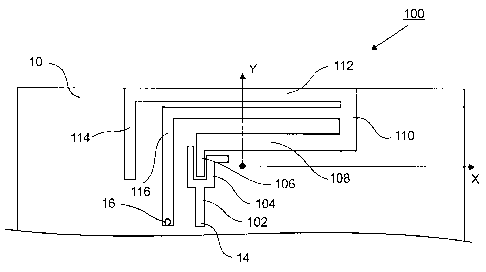
Referring to Figures la and lb, multi-band antenna 100 for sending/receiving
wireless
communication signals in a plurality of frequency bands according to a
preferred embodiment of
the invention is provided. Preferably, the multi-band antenna 100 is
implemented as a PIFA ¨ as
described hereinbelow ¨ but, as will become evident to one skilled in the art,
is not limited
thereto. The multi-band antenna 100 is disposed on the surface of dielectric
substrate 10 such as,
for example, a FR4 dielectric substrate, having a ground plane 12 disposed on
a bottom surface
portion thereof. Preferably, a radiating portion of the multi-band antenna 100
is disposed on a top
surface portion of the dielectric substrate 10 above a ground-clear area of
the dielectric substrate
10.
Feed element 102 is electrically connected via feed port 14 to circuitry of
the wireless device for
providing/receiving signals associated with the wireless communication
signals. Preferably, the
radiating portion of the multi-band antenna 100 is coupled to the feed element
102 via
interdigitated coupler 104. The interdigitated coupler 104 forms, for example,
a three-finger
structure with one end portion having substantially an L-shape and the other
end portion portions
forming open ends. Alternatively, the interdigitated coupler 104 comprises
more than three
fingers and/or different shapes such as, for example, a V-shape or an arc-
shape. The
interdigitated coupler 104 enhances signal coupling and provides increased
flexibility for
Page 4 of 11
CA 02772367 2012-03-23
impedance matching in the antenna design.
Further alternatively, the radiating portion of the multi-band antenna 100 is
coupled to the feed
element 102 in a different fashion such as, for example, in a direct
connection, thus omitting a
coupling element.
The radiating portion of the multi-band antenna 100 is designed as a stepped-
impedance structure
connected to the feed element 102 via the interdigitated coupler 104. The
stepped-impedance
structure comprises a plurality of concatenated stepped-impedance elements,
for example, five
stepped-impedance elements 106, 108, 110, 112, and 114, as illustrated in
Figure lb. Each
stepped-impedance element has a predetermined impedance Z and a predetermined
electrical
length 0 associated with a resonance mode for sending/receiving wireless
communication
signals in a respective frequency band of the plurality of frequency bands. It
is noted that the
effective impedance Z and effective electrical length 0 of each stepped-
impedance element is
also dependent on the characteristics of adjacent stepped-impedance elements,
providing added
flexibility and potential for miniaturization. For example, the length of a
stepped-impedance
element can be substantially smaller than the expected half-wavelength, if the
characteristics of
adjacent stepped-impedance elements are designed accordingly. Preferably, the
stepped-
impedance structure comprises a plurality of folded stripe lines 106, 108,
110, 112, and 114, as
illustrated in Figure lb.
Shorted element 116 is connected at a first end to one of the stepped-
impedance elements ¨ for
example, stepped-impedance element 110, as illustrated in Figures la and lb ¨
and to the ground
plane 12 at a second end. To connect the shorted element 116 disposed on the
top surface of the
dielectric substrate 10 to the ground plane 12 disposed on the bottom surface
of the dielectric
substrate 10 via aperture 16 is disposed in the dielectric substrate 10 for
accommodating the
shorted element 116 therein. Optionally, the shorted element 116 is connected
to another
stepped-impedance element such as, for example, stepped-impedance element 108
or 112.
Connecting the shorted element 116 to another stepped-impedance element has a
minor effect on
the return loss of the multi-band antenna 100 and possibly necessitates re-
design of the antenna.
Page 5 of 11
CA 02772367 2012-03-23
The multi resonance mode property of the stepped-impedance structure is
determined using
generalized transmission line theory and is characterized by the impedance Z
and the electrical
length 9 of each of the stepped-impedance elements. While each stepped-
impedance element is
designed for sending/receiving wireless communication signals in a respective
frequency band of
the plurality of frequency bands, the effective impedance Z and effective
electrical length 0 of
each stepped-impedance element is also dependent on the characteristics of
adjacent stepped-
impedance elements, i.e. the stepped-impedance structure is determined as a
whole. For example,
adding a new stepped-impedance element affects the characteristics of all
other stepped-
impedance elements of the stepped-impedance structure.
The design of the radiating portion of the multi-band antenna 100 as a stepped-
impedance
structure enables substantial control of high resonance modes by adjusting the
impedances Z and
electrical lengths 9 of the stepped-impedance elements. Furthermore, the
design as a stepped-
impedance structure enables suppressing/filtering of unwanted higher order
resonance modes.
In an exemplary implementation the multi-band antenna 100 has been realized as
a PIFA ¨ as
illustrated in Figures la and lb for sending/receiving wireless communication
signals in five
frequency bands centered at: 915 MHz; 1575 MHz; 2400 MHz; 3200 MHz; and 5800
MHz to
cover: ISM 915/2400/5800 tri-bands; GPS band; and IMT C-band. The ground plane
12 ¨ 73.6
mm long and 54 mm wide ¨ is printed on the bottom surface of the FR4
dielectric substrate 10.
The radiating portion of the multi-band antenna 100 is formed by printing or
etching on the top
surface of the dielectric substrate 10 - which is 85.6 mm long, 54 mm wide,
and 1 mm thick.
Figure 2 illustrates simulated and measured return loss for the multi-band
antenna 100 as
implemented. The experimental result illustrates that the multi-band antenna
100 sends/receives
wireless communication signals in five frequency bands centered at: 915 MHz;
1575 MHz; 2400
MHz; 3200 MHz; and 5800 MHz, associated with the stepped-impedance elements:
106; 108;
110; 112; and 114, respectively. The experimental result also illustrates that
the five frequency
bands are tuned in a substantially optimal fashion absent unwanted higher
order resonance
modes. Therefore, the multi-band antenna 100 enables implementation of an
antenna for
sending/receiving wireless communication signals in a plurality of frequency
bands covering
Page 6 of 11
CA 02772367 2012-03-23
major frequency bands used in state of the art wireless communication.
Furthermore, the stepped-
impedance structure of the multi-band antenna 100 enables design and
implementation of a
multi-band antenna in a substantially compact and simple fashion using
standard technology.
In the exemplary implementation the multi-band antenna 100 was designed having
five stepped-
impedance elements for sending/receiving wireless signals in five respective
frequency bands,
but is not limited thereto. In state of the art technology, the limit to the
number of implementable
frequency bands is determined by the losses in the metallic interconnects
used. State of the art
low loss dielectric substrates such as, for example, Low-Temperature Co-fired
Ceramics (LTCC)
enable design of multi-band antennas for sending/receiving in up to
approximately 12 frequency
bands, while dielectric substrates exhibiting higher losses such as, for
example, FR4, enable
design of multi-band antennas for sending/receiving in a smaller number of
frequency bands. The
implementable maximum frequency for sending/receiving wireless signals is
depending on the
dielectric substrate used with the maximum frequency being approximately 10
GHz for state of
the art dielectric substrates such as, for example, LTCCs. The multi-band
antenna 100 is
implementable for simultaneously sending/receiving wireless signals in
different frequency bands
provided the circuitry connected to the multi-band antenna 100 is capable of
operating in full-
duplex mode.
In the exemplary implementation the multi-band antenna 100 was designed having
five
concatenated stepped-impedance elements with the stepped-impedance elements
being arranged
in order of increased center frequency of the different frequency bands with
stepped-impedance
element 106 being associated with the lowest center frequency as illustrated
in Figure 2. It is
noted that the design of the multi-band antenna 100 is not limited thereto,
i.e. the stepped-
impedance elements can be arranged in an arbitrary fashion, for example, in
dependence upon an
available surface area on the dielectric substrate 10.
The implementation the multi-band antenna 100 is not limited to the stepped-
impedance
elements being disposed on a single surface of the dielectric substrate 10.
For example,
depending on the surface area available on the dielectric substrate 10, the
stepped-impedance
elements are disposed on different surfaces ¨ for example, the top surface, a
side surface, and the
Page 7 of 11
CA 02772367 2012-03-23
bottom surface - of the dielectric substrate 10, as illustrated in Figures 3a
to 3c.
The stepped-impedance elements are implementable in a plurality of shapes such
as, for example,
circles, ellipses, rectangles, and triangles, with the shapes being arranged
in an arbitrary order, as
illustrated in Figure 4b with stepped-impedance elements 208, 210, 212, 214,
216, and 218.
Optionally, a plurality of stepped-impedance structures is branched off a same
feed line with each
stepped-impedance structure being capable of sending/receiving wireless
signals in a plurality
different frequency bands up to a maximum number of different frequency bands
depending on
the dielectric substrate used.
Further optionally, as illustrated in Figure 4b, the stepped-impedance
elements 308, 310, and 312
are not directly concatenated but connected via connecting elements 314.
The present invention has been described herein with regard to preferred
embodiments. However,
it will be obvious to persons skilled in the art that a number of variations
and modifications can
be made without departing from the scope of the invention as described herein.
Page 8 of 11