Note: Descriptions are shown in the official language in which they were submitted.
CA 02774838 2012-03-21
WO 2011/036446
PCT/GB2010/001782
ENCAPSULATED SEMICONDUCTOR NANOPARTICLE - BASED MATERIALS
COMPRISING AN ADDITIVE
The present invention relates to semiconductor nanoparticle-based materials,
particularly, but not exclusively, quantum dot-containing beads for use in the
fabrication of quantum dot-based light emitting devices.
There has been substantial interest in exploiting the properties of compound
semiconductors consisting of particles with dimensions in the order of 2-50
nm, often
referred to as quantum dots (QDs) or nanocrystals. These materials are of
commercial interest due to their size-tuneable electronic properties which can
be
exploited in many commercial applications such as optical and electronic
devices and
other applications that ranging from biological labelling, photovoltaics,
catalysis,
biological imaging, LEDs, general space lighting and electroluminescent
displays
amongst many new and emerging applications.
The most studied of semiconductor materials have been the chalcogenides II-VI
materials namely ZnS, ZnSe, CdS, CdSe, CdTe; most noticeably CdSe due to its
tuneability over the visible region of the spectrum. Reproducible methods for
the
large scale production of these materials have been developed from "bottom up"
techniques, whereby particles are prepared atom-by-atom, i.e. from molecules
to
clusters to particles, using "wet" chemical procedures.
Two fundamental factors, both related to the size of the individual
semiconductor
nanoparticle, are responsible for their unique properties. The first is the
large surface
to volume ratio; as a particle becomes smaller, the ratio of the number of
surface
atoms to those in the interior increases. This leads to the surface properties
playing
an important role in the overall properties of the material. The second factor
being,
with many materials including semiconductor nanoparticles, that there is a
change in
the electronic properties of the material with size, moreover, because of
quantum
confinement effects the band gap gradually becomes larger as the size of the
particle
decreases. This effect is a consequence of the confinement of an 'electron in
a box'
giving rise to discrete energy levels similar to those observed in atoms and
molecules, rather than a continuous band as observed in the corresponding bulk
semiconductor material. Thus, for a semiconductor nanoparticle, because of the
physical parameters, the "electron and hole", produced by the absorption of
electromagnetic radiation, a photon, with energy greater then the first
excitonic
transition, are closer together than they would be in the corresponding
CA 02774838 2012-03-21
WO 2011/036446
PCT/GB2010/001782
macrocrystalline material, moreover the Coulombic interaction cannot be
neglected.
This leads to a narrow bandwidth emission, which is dependent upon the
particle size
and composition of the nanoparticle material. Thus, quantum dots have higher
kinetic
energy than the corresponding macrocrystalline material and consequently the
first
excitonic transition (band gap) increases in energy with decreasing particle
diameter.
Core semiconductor nanoparticles, which consist of a single semiconductor
material
along with an outer organic passivating layer, tend to have relatively low
quantum
efficiencies due to electron-hole recombination occurring at defects and
dangling
bonds situated on the nanoparticle surface which can lead to non-radiative
electron-
hole recombinations. One method to eliminate defects and dangling bonds on the
inorganic surface of the quantum dot is to grow a second inorganic material,
having a
wider band-gap and small lattice mismatch to that of the core material
epitaxially on
the surface of the core particle, to produce a "core-shell" particle. Core-
shell particles
separate any carriers confined in the core from surface states that would
otherwise
act as non-radiative recombination centres. One example is a ZnS shell grown
on the
surface of a CdSe core. Another approach is to prepare a core-multi shell
structure
where the "electron-hole" pair is completely confined to a single shell layer
consisting
of a few monolayers of a specific material such as a quantum dot-quantum well
structure. Here, the core is of a wide band gap material, followed by a thin
shell of
narrower band gap material, and capped with a further wide band gap layer,
such as
CdS/HgS/CdS grown using substitution of Hg for Cd on the surface of the core
nanocrystal to deposit just a few monolayers of HgS which is then over grown
by a
monolayer of CdS. The resulting structures exhibit clear confinement of photo-
excited
carriers in the HgS layer. To add further stability to quantum dots and help
to confine
the electron-hole pair one of the most common approaches is by epitaxially
growing
a compositionally graded alloy layer on the core this can help to alleviate
strain that
could otherwise led to defects. Moreover for a CdSe core in order to improve
structural stability and quantum yield, rather growing a shell of ZnS directly
on the
core a graded alloy layer of Cdi.xZn.Sei_ySy can be used. This has been found
to
greatly enhance the photoluminescence emission of the quantum dots.
Doping quantum dots with atomic impurities is an efficient way also of
manipulating
the emission and absorption properties of the nanoparticle. Procedures for
doping of
wide band gap materials, such as zinc selenide and zinc sulfide, with
manganese
and copper (ZnSe:Mn or ZnS:Cu), have been developed. Doping with different
luminescence activators in a semiconducting nanocrystal can tune the
2
CA 02774838 2012-03-21
WO 2011/036446
PCT/GB2010/001782
photoluminescence and electroluminescence at energies even lower than the band
gap of the bulk material whereas the quantum size effect can tune the
excitation
energy with the size of the quantum dots without having a significant change
in the
energy of the activator related emission.
The widespread exploitation of quantum dot nanoparticles has been restricted
by
their physical/chemical instability and incompatibility with many of the
materials
and/or processes required to exploit the quantum dots to their full potential,
such as
incorporation into solvents, inks, polymers, glasses, metals, electronic
materials,
electronic devices, bio-molecules and cells. Consequently, a series of quantum
dot
surface modification procedures has been employed to render the quantum dots
more stable and compatible with the materials and/or processing requirements
of a
desired application.
A particularly attractive potential field of application for quantum dots is
in the
development of next generation light-emitting diodes (LEDs). LEDs are becoming
increasingly important in modern day life and it is envisaged that they have
the
potential to become one of the major applications for quantum dots, in for
example,
automobile lighting, traffic signals, general lighting, liquid crystal display
(LCD)
backlighting and display screens.
Currently, LED devices are made from inorganic solid-state compound
semiconductors, such as AlGaAs (red), AlGaInP (orange-yellow-green), and
AlGaInN
(green-blue), however, using a mixture of the available solid-state compound
semiconductors, solid-state LEDs which emit white light cannot be produced.
Moreover, it is difficult to produce "pure" colours by mixing solid-state LEDs
of
different frequencies. Therefore, currently the main method of colour mixing
to
produce a required colour, including white, is to use a combination of
phosphorescent materials which are placed on top of the solid-state LED
whereby
the light from the LED (the "primary light") is absorbed by the phosphorescent
material and then re-emitted at a different frequency (the "secondary light"),
i.e. the
phosphorescent materials down convert the primary light to the secondary
light.
Moreover, the use of white LEDs produced by phosphor down-conversion leads to
lower cost and simpler device fabrication than a combination of solid-state
red-green-
blue LEDs.
3
CA 02774838 2012-03-21
WO 2011/036446
PCT/GB2010/001782
Current phosphorescent materials used in down converting applications absorb
UV
or mainly blue light and converts it to longer wavelengths, with most
phosphors
currently using trivalent rare-earth doped oxides or halophosphates. White
emission
can be obtained by blending phosphors which emit in the blue, green and red
regions
with that of a blue or UV emitting solid-state device. i.e. a blue light
emitting LED plus
a green phosphor such as, SrGa2S4:Eu2+, and a red phosphor such as, SrSiEu2*
or a
UV light emitting LED plus a yellow phosphor such as, Sr2P207:Eu2+;Mu2+, and a
blue-green phosphor. White LEDs can also be made by combining a blue LED with
a yellow phosphor, however, colour control and colour rendering is poor when
using
this methodology due to lack of tunability of the LEDs and the phosphor.
Moreover,
conventional LED phosphor technology uses down converting materials that have
poor colour rendering (i.e. colour rendering index (CRI) <75).
Rudimentary quantum dot-based light emitting devices have been made by
embedding colloidally produced quantum dots in an optically clear (or
sufficiently
transparent) LED encapsulation medium, typically a silicone or an acrylate,
which is
then placed on top of a solid-state LED. The use of quantum dots potentially
has
some significant advantages over the use of the more conventional phosphors,
such
as the ability to tune the emission wavelength, strong absorption properties
and low
scattering if the quantum dots are mono-dispersed.
For the commercial application of quantum dots in next-generation light
emitting
devices, the quantum dots should be incorporated into the LED encapsulating
material while remaining as fully mono-dispersed as possible and without
significant
loss of quantum efficiency. The methods developed to date are problematic, not
least
because of the nature of current LED encapsulants. Quantum dots can
agglomerate
when formulated into current LED encapsulants thereby reducing the optical
performance of the quantum dots. Moreover, even after the quantum dots have
been
incorporated into the LED encapsulant, oxygen can still migrate through the
encapsulant to the surfaces of the quantum dots, which can lead to photo-
oxidation
and, as a result, a drop in quantum yield (QY).
In view of the significant potential for the application of quantum dots
across such a
wide range of applications, including but not limited to, quantum dot-based
light
emitting devices, work has already been undertaken by various groups to try to
develop methods to increase the stability of quantum dots so as to make them
brighter, more long-lived and/or less sensitive to various types of processing
4
CA 02774838 2016-04-12
conditions. For example, reasonably efficient quantum dot-based light emitting
devices can be fabricated under laboratory conditions building on current
published
methods, however, there remain significant challenges to the development of
quantum dot-based materials and methods for fabricating quantum dot-based
devices, such as light emitting devices, on an economically viable scale and
which
would provide sufficiently high levels of performance to satisfy consumer
demand.
Summary Of The Invention
An object of the present invention is to obviate or mitigate one or more of
the above
problems with semiconductor nanoparticle¨based materials and/or current
methods
for fabricating such materials.
A first aspect of the present invention provides a primary particle comprised
of a
primary matrix material containing a population of semiconductor
nanoparticles,
wherein each primary particle further comprises an additive to enhance the
physical,
chemical and/or photo-stability of the semiconductor nanoparticles.
The current invention thus provides a means by which the robustness, and
consequently, the performance of semiconductor nanoparticles can be improved
for
use in a wide range of applications, particularly, but not exclusively the
fabrication of
semiconductor nanoparticle-based light emitting devices, preferably where the
device
incorporates an LED as a primary light source and the semiconductor
nanoparticles
as a secondary light source. By providing each primary particle with one or
more
stability enhancing additives, the semiconductor nanoparticles are less
sensitive to
their surrounding environment and subsequent processing steps.
In a preferred embodiment a plurality of quantum dots are incorporated into
one or
more silica beads which also include a free-radial scavenger, such as
benzophenone
or a derivative thereof, which quantum dot-containing beads are then embedded
or
entrapped within a host LED encapsulation material such as a silicone, an
epoxy
resin, a (meth)acrylate or a polymeric material.
1
CA 02774838 2015-12-15
The term "bead" is used herein for convenience and is not intended to impose
any
particular size or shape limitation to the material described as a "bead".
Thus, for
example, the beads may be spherical but other configurations are possible.
Where
reference is made herein to ''microbeads" this is intended to refer to "beads"
as
defined above having a dimension on the micron scale.
The or each primary particle may be provided with a separate layer of a
surface
coating material. The term "coating" is used herein to refer to one or more
layers of
material provided on another material, which may partially or fully cover the
exterior
surface or solvent accessible surface of that other material. The material of
the
"coating" may penetrate at least partially into the internal structure of the
material to
which it has been applied, provided the coating still affords a level of
protection or
functions in some way as a barrier to the passage of potentially harmful
species, e.g.
oxygen, through the coated material. It will be appreciated from the wording
used to
define the various aspects of the present invention herein that the "coating"
applied to
each primary particle results in the production of a plurality of separate,
distinct
coated particles rather than a plurality of particles contained or
encapsulated within
the same, unitary matrix-type material, such as a plurality of resin beads
dispersed
throughout an LED encapsulant.
The nanoparticle-containing primary particles or beads are preferably provided
in the
form of microbeads. By pre-loading small microbeads, which can range in size
from
50 nm to 500 pm or more preferably 25 nm to 0.1 mm or more preferably still 20
nm
to 0.5 mm in diameter, with quantum dots, adding an additive, and then
optionally
providing a surface coating of, for example, a polymer or oxide material, the
resulting
beads are more stable towards their surrounding environment and/or subsequent
processing conditions, such as the incorporation of the quantum dot-containing
beads into an LED encapsulation material on a UV or blue LED. As a result, not
only
does handling of the quantum dots become easier, but their optical performance
can
be improved and it can become simpler to tune the colour of the light they
emit, for
example when used in an LED-based device. Moreover, this approach is simpler
than attempting to incorporate quantum dots directly into an LED encapsulate
(for
example, a silicone, an epoxy, a (meth)acrylate, a polymeric material or the
like) in
6
CA 02774838 2012-03-21
WO 2011/036446
PCT/GB2010/001782
terms of ease of colour rendering, processing, and reproducibility and offers
greater
quantum dot stability to photo-oxidation.
The quantum dot-containing beads can be made to any desirable size, such as
the
same size as currently employed YAG phosphor materials which range from 10 to
100pm and can thus be supplied to existing LED manufacturers in a similar form
to
that of the current commercially used phosphor materials. Moreover, the
quantum
dot-containing beads incorporating the additive(s) is (are) in a form that is
compatible
with the existing LED fabrication infrastructure.
With the advantage of very little or no loss of quantum dot quantum yield (QY)
in
processing; this new approach of optionally coated quantum dot-containing
beads
incorporating stability-enhancing additives leads to less loss of quantum
efficiency
than when formulating the quantum dots directly into a LED encapsulation
medium or
when using quantum dot beads not incorporating such additives or a protective
surface coating. Because there is very little or no loss of quantum yield it
is easier to
colour render and less binning is required. It has been shown that when
formulating
quantum dots directly into an encapsulation medium using prior art methods,
colour
control is very difficult due to quantum dot re-absorption or loss of quantum
yield and
shifting of the PL max position. Moreover batch to batch, i.e. device-to-
device,
reproducibility is very difficult or impossible to achieve. By pre-loading the
quantum
dots into one or more beads also incorporating the stability-enhancing
additive(s),
and then optionally coating the beads, the colour of the light emitted by the
device is
of higher quality, easier to control and is more reproducible.
By incorporating known amounts of quantum dots into beads also incorporating
stability-enhancing additives, and optionally providing the beads with a
protective
surface coating, migration of deleterious species, such as moisture, oxygen
and/or
free radicals, is eliminated or at least reduced, thereby eliminating or at
least
minimising these common hurdles to the industrial production of quantum dot
based
materials and devices.
A second aspect of the present invention provides a method for preparing a
primary
particle comprised of a primary matrix material, a population of semiconductor
nanoparticles and an additive to enhance the physical, chemical and/or photo-
stability of the semiconductor nanoparticles, the method comprising combining
said
7
CA 02774838 2012-03-21
WO 2011/036446
PCT/GB2010/001782
semiconductor nanoparticles, primary matrix material and additive under
conditions
suitable to produce said primary particle.
An additive may be combined with "naked" semiconductor nanoparticles and
precursors to the primary matrix material during initial production of the
primary
particles. Alternatively, or additionally, an additive may be added after the
semiconductor nanoparticles have been entrapped within the primary matrix
material.
The quantum-dot containing primary particles incorporating an additive can be
dispersed in a secondary matrix material, which may be the same or different
to the
primary matrix material.
A further aspect of the present invention provides a composite material
incorporating
a plurality of primary particles according to the first aspect of the present
invention
dispersed within a secondary matrix material.
A still further aspect provides a light emitting device including a primary
light source
in optical communication with a formulation comprising a composite material
according to the above further aspect embedded in a host light emitting diode
encapsulation medium.
The secondary matrix material may be selected from the group of primary matrix
materials set out above. By way of example, the secondary matrix material may
comprise a material selected from the group consisting of a polymer, a resin,
a
monolith, a glass, a sol gel, an epoxy, a silicone and a (meth)acrylate.
Additionally, the secondary matrix material may be formed into one or more
secondary particles containing one or more primary particles. The secondary
particles may be provided with ifurther additive in a similar manner to that
described
herein in respect of additives added to the primary particles. Accordingly,
the
secondary matrix material may be in the form of one or more secondary
particles and
the or each secondary particle may be provided with a further stability-
enhancing
additive, which may be the same or different to the one or more additives
present in
the primary particles.
Alternatively, the quantum dots may first be captured within one or more types
of
matrix material, such as one or more types of polymeric bead, and then each of
8
i
CA 02774838 2015-12-15
those beads, or beads within beads, may be contained within a primary matrix
material to form the primary particles of the first and second aspects of the
present
invention, which incorporate a stability-enhancing additive. Thus, the
semiconductor
nanoparticles contained within the primary matrix material may be naked"
nanoparticles, or may already be contained within one or more layers of matrix
material before being captured within the primary matrix material and coated.
9
CA 02774838 2016-04-12
According to an aspect of the present invention there is provided a composite
material comprising:
(a) a particle comprising:
a microbead comprising a primary matrix material;
a population of semiconductor nanoparticles contained within the
microbead, the nanoparticles comprising at least one surface-bound ligand;
a first additive to enhance the physical, chemical and/or photo-stability of
the
semiconductor nanoparticles and,
a surface coating disposed on the surface of the microbead; wherein, the
primary matrix material, the surface bound ligand, the additive, and the
surface
coating are different materials; and
(b) a secondary matrix material in the form of one or more secondary
particles containing one or more secondary additives to enhance the physical,
chemical and/or photo-stability of the semiconductor nanoparticles, wherein
(c) the particle of (a) is dispersed within the secondary matrix material of
(b)
and wherein the first additive and the one or more secondary additives are the
same
or different.
According to another aspect of the present invention there is provided a light-
emitting
device including a primary light source in optical communication with a
formulation
comprising a composite material as described herein embedded in a host light-
emitting diode encapsulation medium.
According to another aspect of the present invention there is provided a
composite
material comprising:
(a) a particle comprising:
a microbead comprising a primary matrix material;
a population of semiconductor nanoparticles contained within the
microbead, the nanoparticles comprising at least one surface-bound ligand; and
a first additive to enhance the physical, chemical and/or photo-stability of
the
semiconductor nanoparticles wherein, the primary matrix material, the surface
bound
ligand and the first additive are different materials; and
(b) a secondary matrix material in the form of one or more secondary
particles containing one or more secondary additives to enhance the physical,
chemical and/or photo-stability of the semiconductor nanoparticles, wherein
the
additive is a reducing agent, a free radical scavenger, or a hydride reactive
agent,
and wherein (c) the particle of (a) is dispersed within the secondary matrix
material
of (b) and wherein the first additive and the secondary additives are the same
or
different.
CA 02774838 2016-04-12
A Brief Description Of The Drawings
The present invention is illustrated with reference to the following non-
limiting
examples and figures in which:
Figure 1 schematically depicts a quantum dot-based light emitting device
according
to an aspect of the present invention;
Figure 2 is a 2 CIE 1931 chromaticity diagram;
Figure 3 is a 2 CIE 1931 colour matching diagram matching functions x, y, z;
Figure 4 is a schematic representation of an additive-containing QD-bead-based
light
emitting device employing multi-coloured, multiple quantum dot types in each
bead
such that each bead emits white secondary light;
Figure 5 is a schematic representation of an additive-containing QD-bead-based
light
emitting device employing multi-coloured, multiple quantum dot types in
different
beads such that each bead contains a single quantum dot type emitting a single
colour, a mixture of the beads combining to produce white secondary light;
Figure 6 is a schematic representation of an additive-containing QD-bead-based
light
emitting device employing a singly coloured, single quantum dot type in all
beads
such that a mixture of the beads emits a single colour of secondary light (in
this case,
red light);
Figure 7 is a schematic representation of a process according to a first
embodiment
of the present invention wherein an additive is combined with a population of
quantum dots during formation of a primary particle containing the quantum
dots and,
consequently, the additive;
Figure 8 is a schematic representation of a process according to a second
embodiment of the present invention wherein quantum dots are first
encapsulated
within a bead formed of a first type of polymer (polymer 1) and then an
additive is
combined with the quantum dot-containing bead during formation of a primary
particle made from a second type of polymer (polymer 2) containing the quantum
dot-
containing bead and, consequently, the additive;
10a
CA 02774838 2016-04-12
Figure 9 is a schematic representation of a process according to a third
embodiment
of the present invention wherein quantum dots are first encapsulated within a
population of beads formed of a first type of polymer (polymer 1) and then an
additive
is combined with the quantum dot-containing beads during formation of a
primary
particle made from a second type of polymer (polymer 2) containing the quantum
dot-
containing beads and, consequently, the additive;
Figure 10 is a schematic representation of a process according to a fourth
embodiment of the present invention wherein quantum dots are first
encapsulated
within a population of beads formed of a first type of polymer (polymer 1),
which are
then encapsulated within a bead formed of a second type of polymer (polymer
2),
and then an additive is combined with the quantum dot-containing beads during
formation of a primary particle made from a third type of polymer (polymer 3)
containing the quantum dot-containing beads and, consequently, the additive;
Figure 11 is a schematic representation of a population of quantum dots
entrapped
within a primary particle in the form of a polymer bead according to a
preferred
embodiment of the present invention in which the primary particle is provided
with a
surface coating of an inorganic material, and the primary particles are
dispersed
within a secondary matrix material in the form of an LED encapsulant disposed
on an
LED to provide a light emitting device according to a preferred embodiment of
the
present invention;
Figure 12 is a schematic representation of a population of quantum dots
entrapped
within a primary particle in the form of a polymer bead made from a first type
of
polymer (polymer 1) which is encapsulated within a second type of polymer
material
(polymer 2) which is provided with a surface coating of an inorganic material
according to a preferred embodiment of the present invention, and the
encapsulated
primary particles are dispersed within a secondary matrix material in the form
of an
LED encapsulant disposed on an LED to provide a light emitting device
according to
a preferred embodiment of the present invention;
Figure 13 is a schematic representation of a population of quantum dots
entrapped
within a population of primary particles in the form of polymer beads (bead 1)
according to a preferred embodiment of the present invention in which each of
the
primary particles is provided with a surface coating of an inorganic material,
before
dispersing the coated primary particles within a second type of bead (bead 2)
to
produce a "bead-in-bead" composite material, and then dispersing the bead-in-
bead
composite material within a secondary matrix material in the form of an LED
encapsulant disposed on an LED to provide a light emitting device according to
a
preferred embodiment of the present invention; and
10b
CA 02774838 2016-04-12
Figure 14 is a schematic representation of a population of quantum dots
entrapped
within a population of primary particles in the form of polymer beads
according to a
preferred embodiment of the present invention, the population of primary
particles
being dispersing within a second type of bead to produce a "bead-in-bead"
composite
material which is then provided with an inorganic surface coating layer, and
then
dispersing the bead-in-bead composite material within a secondary matrix
material in
the form of an LED encapsulant disposed on an LED to provide a light emitting
device according to a preferred embodiment of the present invention.
Detailed Description
Primary Matrix Material
The primary matrix material is preferably an optically transparent medium,
i.e. a
medium through which light can pass, and which may be, but does not have to be
substantially optically clear. The primary matrix material, preferably in the
form of a
bead or microbead, may be a resin, polymer, monolith, glass, sol gel, epoxy,
silicone,
(meth)acrylate or the like, or may comprise silica.
Examples of preferred primary matrix materials include acrylate polymers (e.g.
polymethyl(meth)acrylate, polybutylmethacrylate,
polyoctylmethacrylate,
alkylcyanoacryaltes, polyethyleneglycol dimethacrylate, polyvinylacetate etc),
epoxides (e.g., EPOTEK 301 A+ B Thermal curing epoxy, EPOTEK 0G112-4 single
pot UV curing epoxy, or EX0135A and B Thermal curing epoxy), polyamides,
polyimides, polyesters, polycarbonates, polythioethers, polyacrylonitryls,
polydienes,
polystyrene polybutadiene copolymers (Kratons), pyrelenes, pol y-pa r a-
xylyl en e ( parylenes), silica, silica-acrylate hybrids, polyetheretherketone
(PEEK),
polyvinylidene fluoride (PVDF), polydivinyl benzene, polyethylene,
polypropylene,
polyethylene terephthalate (PET), polyisobutylene (butyl rubber),
polyisoprene, and
cellulose derivatives (methyl Cellulose, ethyl cellulose, hydroxypropylmethyl
cellulose,
hydroxypropylmethylcellulose phthalate, nitrocellulose), and combinations
thereof.
Stability-Enhancing Additives
The additives which may be added singly or in any desirable combination to the
primary particles containing the semiconductor nanoparticles can be grouped
according to their intended function as follows:
10c
CA 02774838 2016-04-12
a. Mechanical sealing: Fumed silica (e.g.,Cab-O-SilTm), ZnO, Ti02, ZrO, Mg
stearate, Zn Stearate, all used as a filler to provide mechanical sealing
and/or reduce porosity;
b. Capping agents: Tetradecyl phosphonic acid (TDPA), oleic acid, stearic
acid, polyunsaturated fatty acids, sorbic acid. Zn methacrylate, Mg
1 Od
CA 02774838 2012-03-21
WO 2011/036446
PCT/GB2010/001782
stearate, Zn Stearate, isopropyl myristate. Some of these have multiple
functionality and can act as capping agents, free radical scavengers
and/or reducing agents;
c. Reducing agents: Ascorbic acid palmitate, alpha tocopherol (vitamin E),
octane thiol, butylated hydroxyanisole (BHA), butylated hydroxytoluene
(BHT), gallate esters (propyl, lauryl, octyl and the like), and a
metabisulfite
(e.g. the sodium or potassium salt);
d. Free radical scavengers: benzophenones; and
e. Hydride reactive agents: 1,4-butandiol, 2-hydroxyethyl methacrylate, allyl
methacrylate, 1,6 heptadiene-4-ol, 1,7 octadiene, and 1,4 butadiene.
The selection of the additive or additives for a particular application will
depend upon
the nature of the semiconductor nanoparticle material (e.g. how sensitive the
nanoparticle material is to physical, chemical and/or photo-induced
degradation), the
nature of the primary matrix material (e.g. how porous it is to potentially
deleterious
species, such as free-radicals, oxygen, moisture etc), the intended function
of the
final material or device which will contain the primary particles (e.g. the
operating
conditions of the material or device), and the process conditions required to
fabricate
said final material or device. Thus, with prior knowledge of the above risk-
factors, one
or more appropriate additives can be selected from the above five lists to
suit any
desirable semiconductor nanoparticle application.
Primary Particle Surface Coating Materials
One of the intended functions of the coating which may be provided on the
primary
particles is to provide each primary particle with a protective barrier to
prevent the
passage or diffusion of potentially deleterious species, e.g. oxygen, moisture
or free
radicals, from the external environment through the primary matrix material to
the
semiconductor nanoparticles. As a result, the semiconductor nanoparticles are
less
sensitive to their surrounding environment and the various processing
conditions
typically required to utilise the nanoparticles in applications such as the
fabrication of
LED-based light emitting devices.
The coating is preferably a barrier to the passage of oxygen or any type of
oxidising
agent through the primary matrix material. The coating may be a barrier to the
1
CA 02774838 2012-03-21
WO 2011/036446
PCT/GB2010/001782
passage of free radical species through the primary matrix material, and/or is
preferably a moisture barrier so that moisture in the environment surrounding
the
primary particles cannot contact the semiconductor nanoparticles within the
primary
particles.
The coating may provide a layer of coating material on a surface of the
primary
particle of any desirable thickness provided it affords the required level of
protection.
The surface layer coating may be .around 1 to 10 nm thick, up to around 400 to
500
nm thick, or more. Preferred layer thicknesses are in the range 1 nm to 200
nm, more
preferably around 5 to 100 nm.
In a first preferred embodiment, the coating comprises an inorganic material,
such as
a dielectric (insulator), a metal oxide, a metal nitride or a silica-based
material (e.g. a
glass).
The metal oxide may be a single metal oxide (i.e. oxide ions combined with a
single
type of metal ion, e.g. A1203), or may be a mixed metal oxide (i.e. oxide ions
combined with two or more types of metal ion, e.g. SrTiO3). The metal ion(s)
of the
(mixed) metal oxide may be selected from any suitable group of the periodic
table,
such as group 2, 13, 14 or 15, or may be a transition metal, d-block metal, or
lanthanide metal.
Preferred metal oxides are selected from the group consisting of A1203, B203,
Co203,
Cr203, CuO, Fe203, Ge203, Hf02, 1n203, MgO, Nb205, NiO, Si02, Sn02, Ta205,
Zr02, Sc203, Y203, Ge02, La203, Ce02, PrOx = appropriate integer), Nd203,
Sm203, EuOy (y = appropriate integer), Gd203, Dy203, H0203, Er203, Tr11203,
Yb203,
Lu203, SrTiO3, BaTiO3, PbTiO3, PbZr03, BirnTin0 (m = appropriate integer; n =
appropriate integer), BiaSib0 (a = appropriate integer; b = appropriate
integer),
SrTa206, SrBi2Ta209, YSc03, LaA103, NdA103, GdSc03, LaSc03, LaLu03, Er3Ga5013.
Preferred metal nitrides may be selected from the group consisting of BN, AIN,
GaN,
InN, Zr3N4, Cu2N, Hf3N4, SiN, (c = appropriate integer), TiN, Ta3N5, Ti-Si-N,
Ti-Al-N,
TaN, NbN, MoN, WNd (d = appropriate integer), WNeCr (e = appropriate integer;
f =
appropriate integer).
The inorganic coating may comprise silica in any appropriate crystalline form.
12
CA 02774838 2012-03-21
WO 2011/036446
PCT/GB2010/001782
The coating may incorporate an inorganic material in combination with an
organic or
polymeric material. By way of example, in a preferred embodiment, the coating
is an
inorganic / polymer hybrid, such as a silica-acrylate hybrid material.
In a second preferred embodiment, the coating comprises a polymeric material,
which may be a saturated or unsaturated hydrocarbon polymer, or may
incorporate
one or more heteroatoms (e.g. 0, S, N, halo) or heteroatom-containing
functional
groups (e.g. carbonyl, cyano, ether, epoxide, amide and the like).
Examples of preferred polymeric coating materials include acrylate polymers
(e.g.
polymethyl(meth)acrylate, polybutylmethacrylate, polyoctylmethacrylate,
alkylcyanoacryaltes, polyethyleneglycol dimethacrylate, polyvinylacetate etc),
epoxides (e.g., EPOTEK 301 A+ B Thermal curing epoxy, EPOTEK 0G112-4 single
pot UV curing epoxy, or EX0135A and B Thermal curing epoxy), polyamides,
polyimides, polyesters, polycarbonates, polythioethers, polyacrylonitryls,
polydienes,
polystyrene polybutadiene copolymers (Kratons), pyrelenes, p ol y-para-
xyl y le ne ( parylenes), polyetheretherketone (PEEK), polyvinylidene fluoride
(PVDF), polydivinyl benzene, polyethylene, polypropylene, polyethylene
terephthalate (PET), polyisobutylene (butyl rubber), polyisoprene, and
cellulose
derivatives (methyl cellulose, ethyl cellulose, hydroxypropylmethyl cellulose,
hydroxypropylmethylcellulose phthalate, nitrocellulose), and combinations
thereof.
By incorporating quantum dots into primary particle materials of the kind
described
above and coating the particles it is possible to protect the otherwise
reactive
quantum dots from the potentially damaging surrounding chemical environment.
Moreover, by placing a number of quantum dots into a single bead, for example
in
the size range from 20 nm to 500 pm in diameter, and providing the bead with a
suitable protective coating of, for example, a polymeric or inorganic
material, the
resulting coated QD-bead is more stable than either free "naked" quantum dots,
or
uncoated QD-beads to the types of chemical, mechanical, thermal and/or photo-
processing steps which are required to incorporate quantum dots in most
commercial
applications, such as when employing quantum dots as down converters in a "QD-
solid-state-LED" light emitting device.
Each primary particle may contain any desirable number and/or type of
semiconductor nanoparticles. Thus, the primary matrix material of the primary
particle may contain a single type of semiconductor nanoparticle, e.g. InP,
InP/ZnS or
13
CA 02774838 2012-03-21
WO 2011/036446
PCT/GB2010/001782
CdSe, of a specific size range, such that the plurality of QD-containing beads
emits
monochromatic light of a pre-defined wavelength, i.e. colour. The colour of
the
emitted light may be adjusted by varying the type of semiconductor
nanoparticle
material used, e.g. changing the size of the nanoparticle, the nanoparticle
core
semiconductor material and/or adding one or more outer shells of different
semiconductor materials.
Moreover, colour control can also be achieved by incorporating different types
of
semiconductor nanoparticles, for examples nanoparticles of different size
and/or
chemical composition within the primary matrix material of each particle.
Furthermore, the colour and colour intensity can be controlled by selecting an
appropriate number of semiconductor nanoparticles within each particle.
Preferably
each primary particle contains at least around 1000 semiconductor
nanoparticles of
one or more different types, more preferably at least around 10,000, more
preferably
at least around 50,000, and most preferably at least around 100,000
semiconductor
nanoparticles of one or more different types.
Where the primary particles are provided in the preferred form of beads or
microbeads, some or all of the beads preferably contain one or more
semiconductor
nanoparticle capable of secondary light emission upon excitation by primary
light
emitted by a primary light source (e.g. an LED).
The primary particles may be dispersed within an encapsulating medium, such as
an
LED encapsulant, to provide a robust QD-containing formulation which can then
safely be used in subsequent processing steps, for example, to deposit a
desired
amount of such a formulation on to an LED chip to provide an QD / LED-based
light
emitting device. Any desirable number of beads may be dispersed or embedded
within the encapsulating medium, for example, the formulation may contain 1 to
10,000 beads, more preferably 1 to 5000 beads, and most preferably 5 to 1000
beads.
It should also be appreciated that the encapsulating medium may have embedded
therein one or more type of semiconductor nanoparticle-containing primary
particles.
That is, two or more different types of primary particles (one or more
containing the
nanoparticles) may be embedded within the same encapsulating medium. In this
way, where the population of nanoparticles contains more than one different
type of
14
CA 02774838 2012-03-21
WO 2011/036446
PCT/GB2010/001782
nanoparticle, the nature of the primary particle can be selected for optimum
compatibility with both the different types of nanoparticles and the
particular medium
used.
Advantages of quantum dot-containing beads incorporating stability-enhancing
additives, optionally also incorporating a surface coating, over free quantum
dots or
uncoated quantum dot-containing beads can include greater stability to air and
moisture, greater stability to photo-oxidation and/or greater stability to
mechanical
processing. Moreover, by pre-loading small microbeads, which can range in size
from a few 50 nm to 500 pm, with quantum dots, adding a stability-enhancing
additive and optionally coating the individual microbeads prior to
incorporating a
plurality of such quantum dot-containing beads into an LED encapsulation
material
on a UV or blue LED, it is a relatively simple process to change, in a
controllable and
reproducible manner, the colour of the light emitted by the resulting LED-
based light
emitting device.
Semiconductor Nanoparticies
Any desirable type of semiconductor nanoparticle may be employed in the
present
invention. In a preferred embodiment, the nanoparticle contains ions, which
may be
selected from any desirable group of the periodic table, such as but not
limited to
group 11, 12, 13, 14, 15 or 16 of the periodic table. The nanoparticles may
incorporate transition metal ions or d-block metal ions. It is preferred that
the
nanoparticles contain first and second ions with the first ion preferably
selected from
group 11, 12, 13 or 14 and the second ion preferably selected from group 14,
15 or
16 of the periodic table. The nanoparticles may contain one or more
semiconductor
material selected from the group consisting of CdO, CdS, CdSe, CdTe, ZnO, ZnS,
ZnSe, ZnTe, InP, InAs, InSb, AIP, AIS, AIAs, AlSb, GaN, GaP, GaAs, GaSb, PbS,
PbSe, Si, Ge, MgS, MgSe, MgTe and combinations thereof. Moreover, the
nanoparticles may be binary, tertiary or quaternary core, core-shell or core-
multi
shell, doped or graded nanoparticles.
Any appropriate method may be employed to produce the semiconductor
nanoparticles employed in the various aspects of the present invention. That
being
said, it is preferred that said semiconductor nanoparticles are produced by
converting
a nanoparticle precursor composition to the material of the nanoparticles in
the
presence of a molecular cluster compound under conditions permitting seeding
and
growth of the nanoparticles on the cluster compound. The method may employ the
CA 02774838 2012-03-21
WO 2011/036446
PCT/GB2010/001782
methodology set out in the applicant's co-pending European patent application
(publication no. EP1743054A).
Conveniently, the nanoparticles incorporate first and second ions and the
nanoparticle precursor composition comprises first and second nanoparticle
precursor species containing the first and second ions respectively which are
combined, preferably in the presence of a molecular cluster compound, as
exemplified below in Synthetic Methods 1.1 and 1.2.
The first and second precursor species may be separate species in the
precursor
composition or may form part of a single molecular species containing both the
first
and second ions.
In the preferred embodiments employing a molecular cluster compound, it is
preferred that the molecular clusters contain third and fourth ions. At least
one of said
third and fourth ions is preferably different to said first and second ions
contained in
the first and second nanoparticle precursor species respectively. The third
and fourth
ions may be selected from any desirable group of the periodic table, such as
but not
limited to group 11, 12, 13, 14, 15 or 16 of the periodic table. The third
and/or fourth
ion may be a transition metal ion or a d-block metal ion. Preferably the third
ion is
selected from group 11, 12, 13 or 14 and the fourth ion is selected from group
14, 15
or 16 of the periodic table.
By way of example, the molecular cluster compound may incorporate third and
fourth
ions from groups 12 and 16 of the periodic table respectively and the first
and second
ions derived from the first and second nanoparticle precursor species may be
taken
from groups 13 and 15 of the periodic table respectively as in Synthetic
Method 1.2.
The methodology described in the applicant's co-pending International PCT
patent
application (application no. PCT/GB2008/002560) may be employed.
It will be appreciated that during the reaction of the first and second
nanoparticle
precursor species, the first nanoparticle precursor species may be added in
one or
more portions and the second nanoparticle precursor species may be added in
one
or more portions. The first nanoparticle precursor species is preferably added
in two
or more portions. In this case, it is preferred that the temperature of a
reaction
mixture containing the first and second nanoparticle precursor species is
increased
between the addition of each portion of the first precursor species.
Additionally or
16
CA 02774838 2012-03-21
WO 2011/036446
PCT/GB2010/001782
alternatively, the second nanoparticle precursor species may be added in two
or
more portions, whereupon the temperature of a reaction mixture containing the
first
and second nanoparticle precursor species may be increased between the
addition
of each portion of the second precursor species. The methodology described in
the
applicant's co-pending European patent application (application no.
06808360.9)
may be used.
The coordination about the final inorganic surface atoms in any core, core-
shell or
core-multi shell, doped or graded nanoparticle is typically incomplete, with
highly
reactive non-fully coordinated atoms acting as "dangling bonds" on the surface
of the
particle, which can lead to particle agglomeration. This problem is typically
overcome
by passivating (capping) the "bare" surface atoms with protecting organic
groups.
In many cases, the capping agent is the solvent in which the nanoparticles
have
been prepared, and consists of a Lewis base compound, or a Lewis base compound
diluted in an inert solvent such as a hydrocarbon. There is a lone pair of
electrons on
the Lewis base capping agent that are capable of a donor type coordination to
the
surface of the nanoparticle; ligands of this kind include, but are not limited
to, mono-
or multi- dentate ligands such as phosphines (trioctylphosphine,
triphenylphosphine,
t-butylphosphine etc.), phosphine oxides (trioctylphosphine oxide,
triphenylphosphine
oxide etc.), alkyl phosphonic acids, alkyl-amines (hexadecylamine, octylamine
etc.),
aryl-amines, pyridines, long chain fatty acids and thiophenes.
In addition to the outermost layer of organic material or sheath material
(capping
agent) helping to inhibit nanoparticle-nanoparticle aggregation, this layer
can also
protect the nanoparticles from their surrounding electronic and chemical
environments, and provide a means of chemical linkage to other inorganic,
biological
or organic material, whereby the functional group is pointing away from the
nanoparticle surface and is available to bond/react/interact with other
available
molecules. Examples include, but are not limited to, amines, alcohols,
carboxylic
acids, esters, acid chloride, anhydrides, ethers, alkyl halides, amides,
alkenes,
alkanes, alkynes, allenes, amino acids, azides, groups etc.. The outermost
layer
(capping agent) of a quantum dot can also consist of a coordinated ligand that
processes a functional group that is polymerisable and can be used to form a
polymer layer around the nanoparticle. The outermost layer can also consist of
organic units that are directly bonded to the outermost inorganic layer such
as via a
disulphide bond between the inorganic surface (e.g. ZnS) and a thiol capping
17
CA 02774838 2012-03-21
WO 2011/036446
PCT/GB2010/001782
molecule. These can also possess additional functional group(s), not bonded to
the
surface of the particle, which can be used to form a polymer around the
particle, or
for further reaction/interaction/chemical linkage.
An example of a material to which nanoparticle surface binding ligands can be
linked
is the primary matrix material from which the primary particles are formed.
There are
a number of approaches to incorporate semiconductor nanoparticles, such as
quantum dots, into the types of primary matrix materials described
hereinbefore by
pre-coating the nanoparticles with ligands that are compatible in some way
with the
matrix material of the primary particles. By way of example, in the preferred
embodiment where the semiconductor nanoparticles are to be incorporated into
polymeric beads, the nanoparticles can be produced so as to possess surface
ligands which are polymerizable, hydrophobic, hydrophilic, positively or
negatively
charged, or functionalised with a reactive group capable of associating with
the
polymer of the polymeric beads by chemical reaction, covalent linkage or non-
covalent interaction (e.g. interchelation).
The inventors have determined that it is possible to take quantum dots
prepared
using any desirable method, incorporate these quantum dots into silica or
polymer
beads also including at least one type of stability-enhancing additive, and
then
optionally coat the beads with a protective barrier layer of a material such
as a
polyacrylate or dielectric metal oxide like aluminium oxide, to provide
significantly
more robust, easily processible quantum dot-containing materials. Quantum dot-
containing beads of this kind can be employed in a wide range of applications,
particularly, but not exclusively, the fabrication of LED-based light emitting
devices
wherein the QD-beads are embedded within a host LED encapsulant and then
deposited onto a solid-state LED chip to form a quantum dot-based light
emitting
device.
Incorporating Quantum Dots into Beads
Considering the initial step of incorporating quantum dots into beads, a first
option is
to incorporate the quantum dots directly into the beads. A second option is to
immobilise the quantum dots in beads through physical entrapment. It is
possible
using these methods to make a population of beads that contain just a single
type of
quantum dot (e.g. one colour) by incorporating a single type of quantum dot
into the
beads. Alternatively, it is possible to construct beads that contain 2 or more
types of
quantum dot (e.g. two or more colours) by incorporating a mixture of two or
more
18
CA 02774838 2012-03-21
WO 2011/036446
PCT/GB2010/001782
types of quantum dot (e.g. material and/or size) into the beads. Such mixed
beads
can then be combined in any suitable ratio to emit any desirable colour of
secondary
light following excitation by the primary light emitted by the primary light
source (e.g.
LED). This is exemplified in Figures 4 to 6 below which schematically show QD-
bead
light emitting devices including respectively: a) multi-coloured, multiple
quantum dot
types in each bead such that each bead emits white secondary light; b) multi-
coloured, multiple quantum dot types in different beads such that each bead
contains
a single quantum dot type emitting a single colour, a mixture of the beads
combining
to produce white secondary light; and c) singly coloured, single quantum dot
type in
all beads such that a mixture of the beads emits a single colour of secondary
light,
e.g. red.
The or each stability-enhancing additive may be added to the quantum dot-
containing
beads during initial bead formation and/or after the beads have been formed
independently of which of the two options set out above are employed to
incorporate
the quantum dots within the beads.
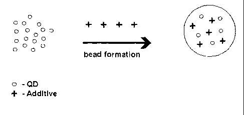
Incorporating Quantum Dots Beads During Bead Formation
With regard to the first option of incorporating the quantum dots directly
into the
primary particles (i.e. the beads) during bead formation, by way of example,
suitable
core, core/shell or core/multishell nanoparticles (e.g. InP/ZnS core/shell
quantum
dots) may be contacted by one or more bead precursors (e.g. an acrylate
monomer,
a silicate material, or a combination of both) and then subjected to suitable
conditions
(e.g. introduction of a polymerisation initiator) to form the bead material.
One or more
stability-enhancing additive may be included in the reaction mixture in which
the
nanoparticles are contacted by the bead precursors. Moreover, at this stage, a
surface coating can be applied to the beads.
By way of further example, hexadecylamine-capped CdSe-based semiconductor
nanoparticles can be treated with at least one, more preferably two or more
polymerisable ligands (optionally one ligand in excess) resulting in the
displacement
of at least some of the hexadecylamine capping layer with the polymerisable
ligand(s). The displacement of the capping layer with the polymerisable
ligand(s) can
be accomplished by selecting a polymerisable ligand or ligands with structures
similar to that of trioctylphosphine oxide (TOPO), which is a ligand with a
known and
very high affinity for CdSe-based nanoparticles. It will be appreciated that
this basic
methodology may be applied to other nanoparticle / ligand pairs to achieve a
similar
19
CA 02774838 2012-03-21
WO 2011/036446
PCT/GB2010/001782
effect. That is, for any particular type of nanoparticle (material and/or
size), it is
possible to select one or more appropriate polymerisable surface binding
ligands by
choosing polymerisable ligands comprising a structural motif which is
analogous in
some way (e.g. has a similar physical and/or chemical structure) to the
structure of a
known surface binding ligand. Once the nanoparticles have been surface-
modified in
this way, they can then be added to a monomer component of a number of
microscale polymerisation reactions to form a variety of quantum dot-
containing
resins and beads.
Examples of polymerisation methods that may be used to construct quantum dot-
containing beads include, but are not limited to, suspension, dispersion,
emulsion,
living, anionic, cationic, RAFT, ATRP, bulk, ring closing metathesis and ring
opening
metathesis. Initiation of the polymerisation reaction may be caused by any
appropriate means that causes the monomers to react with one another, such as
free
radicals, light, ultrasound, cations, anions, heat.
A preferred method is suspension polymerisation involving thermal curing of
one or
more polymerisable monomers from which the primary matrix material is to be
formed. Said polymerisable monomers may, for example, comprise methyl
(meth)acrylate, ethylene glycol dimethacrylate and/or vinyl acetate.
Quantum dot-containing beads may be generated simply by adding quantum dots to
the mixture of reagents used to construct the beads. In some instances quantum
dots
(nascent quantum dots) will be used as isolated from the reaction employed to
synthesise them and are thus generally coated with an inert outer organic
ligand
layer. In an alternative procedure a ligand exchange process may be carried
out
prior to the bead forming reaction. Here one or more chemically reactive
ligands (for
example this might be a ligand for the quantum dots which also contains a
polymerisable moiety) is added in excess to a solution of nascent quantum dots
coated in an inert outer organic layer. After an appropriate incubation time
the
quantum dots are isolated, for example by precipitation and subsequent
centrifugation, washed and then incorporated into the mixture of reagents used
in the
bead forming reaction/process.
Both quantum dot incorporation strategies will result in statistically random
incorporation of the quantum dots into the beads and thus the polymerisation
reaction will result in beads containing statistically similar amounts of the
quantum
CA 02774838 2012-03-21
WO 2011/036446
PCT/GB2010/001782
dots and, optionally, the one or more additives. Bead size can be controlled
by the
choice of polymerisation reaction used to construct the beads, and
additionally, once
a polymerisation method has been selected, bead size can also be controlled by
selecting appropriate reaction conditions, e.g. in a suspension polymerisation
reaction by stirring the reaction mixture more quickly to generate smaller
beads.
Moreover the shape of the beads can be readily controlled by choice of
procedure in
conjunction with whether or not the reaction is carried out in a mould. The
composition of the beads can be altered by changing the composition of the
monomer mixture from which the beads are constructed. Similarly the beads can
also be cross-linked with varying amounts of one or more cross-linking agents
(e.g.
divinyl benzene). If beads are constructed with a high degree of cross-
linking, e.g.
greater than 5 mol% cross-linker, it may be desirable to incorporate a porogen
(e.g.
toluene or cyclohexane) during the reaction used to construct the beads. The
use of
a porogen in such a way leaves permanent pores within the matrix constituting
each
bead. These pores may be sufficiently large to allow the ingress of quantum
dots
into the bead.
Incorporating Quantum Dots into Prefabricated Beads
In respect of the second option for incorporating quantum dots into the
primary
particles, the quantum dots can be immobilised within the primary matrix
material
through physical entrapment. For example, a solution of quantum dots in a
suitable
solvent (e.g. an organic solvent) can be incubated with a sample of primary
particles.
Removal of the solvent using any appropriate method results in the quantum
dots
becoming immobilised within the primary matrix material of the primary
particles.
The quantum dots remain immobilised in the particles unless the sample is
resuspended in a solvent (e.g. organic solvent) in which the quantum dots are
freely
soluble. One or more stability-enhancing additives may, for example, be
included in
the quantum dot solution which is incubated with the primary particles.
Alternatively,
the quantum dots may first be added to the primary particles, and the one or
more
additives then added to the primary particles. Additionally, at this stage, a
surface
coating can be applied to the primary particles if desired.
In a further preferred embodiment, at least a portion of the semiconductor
nanoparticles can be physically attached to the prefabricated primary
particles.
Attachment may be achieved by immobilisation of a portion of the semiconductor
nanoparticles within the polymer matrix of the prefabricated primary particles
or by
chemical, covalent, ionic, or physical connection between the semiconductor
21
CA 02774838 2012-03-21
WO 2011/036446
PCT/GB2010/001782
nanoparticles and the prefabricated primary particles. In a particularly
preferred
embodiment the prefabricated primary particles comprise polystyrene,
polydivinyl
benzene and a polythiol.
Quantum dots can be irreversibly incorporated into prefabricated primary
particles in
a number of ways, e.g. chemical, covalent, ionic, physical (e.g. by
entrapment) or any
other form of interaction. If prefabricated primary particles are to be used
for the
incorporation of quantum dots, the solvent accessible surfaces of the primary
particles may be chemically inert (e.g. polystyrene) or alternatively they may
be
chemically reactive/functionalised (e.g. Merrifield's Resin). The chemical
functionality
may be introduced during the construction of the primary particles, for
example by
the incorporation of a chemically functionalised monomer, or alternatively,
chemical
functionality may be introduced in a post-particle construction treatment
stsep, for
example by conducting a chloromethylation reaction. Additionally chemical
functionality may be introduced by a post-particle construction step involving
a
polymeric graft or other similar process whereby chemically reactive
polymer(s) are
attached to the outer layers/accessible surfaces of the bead. More than one
such
post construction derivatisation process may be carried out to introduce
chemical
functionality onto/into the primary particles.
=
As with quantum dot incorporation into primary particles during the particle
forming
reaction (i.e. the first option described above) the pre-fabricated primary
particles can
be of any shape, size and composition and may have any degree of cross-linker
and
may contain permanent pores if constructed in the presence of a porogen.
Quantum
dots may be imbibed into the primary particles by incubating a solution of
quantum
dots in an organic solvent and adding this solvent to the primary particles.
The
solvent must be capable of wetting the primary particles, and in the case of
lightly
crosslinked primary particles, preferably 0-10 % crosslinked and most
preferably 0-2
% crosslinked, the solvent should cause the polymer matrix to swell in
addition to
solvating the quantum dots. Once the quantum dot-containing solvent has been
incubated with the primary particles it can be removed, for example by heating
the
mixture and causing the solvent to evaporate and the quantum dots to become
embedded in the primary matrix material constituting the primary particles, or
alternatively, by the addition of a second solvent in which the quantum dots
are not
readily soluble but which mixes with the first solvent causing the quantum
dots to
precipitate within the primary matrix material. Immobilisation may be
reversible if the
primary particles are not chemically reactive, or else if the primary
particles are
22
CA 02774838 2012-03-21
WO 2011/036446
PCT/GB2010/001782
chemically reactive, the quantum dots may be held permanently within the
primary
matrix material, by chemical, covalent, ionic, or any other form of
interaction. Any
desirable stability-enhancing additive can be added during any of the stages
of the
quantum dot ¨ bead fabrication described above.
Incorporation of Quantum Dots into Sol-Gels to produce Glass
As stated above, a preferred primary matrix material is an optically
transparent
media, such as a sol-gel or a glass. Such primary matrix materials may be
formed in
an analogous fashion to the method used to incorporate quantum dots into
primary
particles during the particle forming process as described above. For example,
a
single type of quantum dot (e.g. one colour) may be added to a reaction
mixture used
to produce a so-gel or glass. Alternatively, two or more types of quantum dot
(e.g.
two or more colours) may be added to a reaction mixture used to produce a sol-
gel or
glass. The sol-gels and glasses produced by these procedures may have any
shape,
morphology or 3-dimensional structure. For example, the resulting primary
particles
may be spherical, disc-like, rod-like, ovoid, cubic, rectangular, or any of
many other
possible configurations. Any of the stability-enhancing additives described
hereinbefore may be added to quantum dot¨containing glass beads. Some silica-
based beads exhibit relatively low porosity as compared, for example, to
polymeric
resin beads (e.g. acrylate-based beads). It may therefore be advantageous to
add
the or each additive during initial bead formation when the beads are made
from a
silica-based material rather than adding the additive(s) after bead formation,
which
may be more advantageous or desirable when using more porous bead materials.
Application of Optional Surface Coating
In a preferred embodiment, where it is desired to provide a surface coating
comprising an inorganic material on the quantum dot-containing primary
particles,
such as a metal oxide or metal nitride, a particularly preferred process to
deposit the
coating is atomic layer deposition (ALD), although it will be appreciated that
other
=
suitable techniques can be employed.
The provision of a surface coating by ALD, using a metal oxide surface coating
as an
example, comprises the following four basic steps:
1) Exposing a surface of a quantum dot-containing primary particle to a metal
precursor;
23
CA 02774838 2012-03-21
WO 2011/036446
PCT/GB2010/001782
2) Purging the reaction chamber containing the primary particles to remove non-
reacted metal precursor and any gaseous reaction by-products;
3) Exposing the surface of the primary particles to an oxide precursor; and
4) Purging the reaction chamber.
The above steps can then be repeated any desirable number of times to provide
a
surface coating of the desired thickness, for example, a thickness of around 1
to 500
nm. Each reaction cycle adds a predetermined amount of coating material to the
surface of the primary particles. One cycle may take time from around 0.5
seconds to
around 2-3 seconds and deposit between 1 and 30 nm of surface coating.
Before initiating the ALD process, it is preferred that the surface of the
primary
particles is heat treated to ensure their stability during the ALD process. It
will be
appreciated that since ALD is essentially a surface-controlled process, where
process parameters other than the precursors, substrate (i.e. primary particle
material), reaction temperature (typically around 100 to 400 C, but can be as
high as
500 C), and, to a lesser extent pressure (typically around 1 to 10 mbar),
have little or
no influence on the final surface coating, ALD-grown surface layers or films
are
extremely conformal and uniform in thickness, making ALD is a particularly
preferred
method for depositing protective coatings on to the surface of quantum dot-
containing primary particles.
A particularly preferred surface coating is A1203. An A1203 surface coating of
only up
to around 20 to 30 nm applied by ALD at a temperature of around 100 to 175 C
using trimethylaluminium and water as precursors can exhibit a very low water
vapour transmission rate and permeability to other gases and liquids.
It has been determined that ALD coatings applied to quantum dot-containing
primary
particles often result in the deposition of a greater quantity of the surface
coating
material, e.g. A1203 than would be anticipated if the only surface being
coated was
the external surface of the primary particle. It has been established that an
improvement in the level or protection afforded by the surface coating can be
achieved by increasing the amount of surface coating material deposited beyond
the
amount theoretically required to coat just the calculated external surface
area. While
the inventors do not wish to be bound by any particular theory, it is believed
that this
is at least partly due to the ALD process coating not just the external
surface area of
the primary particles, but that it deposits coating material on at least some,
if not
24
CA 02774838 2012-03-21
WO 2011/036446
PCT/GB2010/001782
substantially all of the accessible or effective surface area of the primary
particle
which includes internal voids that are accessible from the outside of the
primary
particle. Thus, when porous, and particularly when highly porous polymeric
bead-
type materials are coated using ALD, it has been observed that the coating
material
is deposited inside the voids and pores of the primary particles, as well as
the
outermost surface of the particles. In this way, the ALD process can be used
to
reduce the porosity of the quantum dot-containing primary particles to
unexpectedly
and surprisingly low levels, thereby providing a degree of protection to the
particles
which is beyond that which would have been anticipated by the skilled person.
This
has important consequencies in terms of the processibility and optical
performance of
the final coated quantum dot-containing primary particles, both of which can
be
greatly enhanced compared to prior art quantum dot-based materials, by the use
of
ALD to provide a surface coating of, for example, A1203.
By way of example, it is known that heat treatment of prior art quantum dot-
containing materials to the temperatures typically required during LED
manufacture
(200 C and above) degrades the performance of the materials to unacceptedly
low
levels. Moreover, the ability to photobrighten such materials is also
significantly
diminished or effectively lost following heat treatment. This places serious
limitations
on the use of quantum dot-based materials in applications such as LED
fabrication,
as well as other manufacturing processes involving heat treatment of
components.
Aspects of the present invention, however, offer convenient solutions to these
problems with prior art materials and methods. By the use of ALD to deposit a
coating material, such as but not limited to A1203, to primary particles
containing
quantum dots it is possible to heat treat the coated materials at temperatures
of up to
at least 250 C and not only do the materials remain structurally sound but it
is
possible photobleach them to substantially restore their original quantum
emission
(i.e. before coating and heat treatment).
In an alternative preferred embodiment, the surface coating may be produced in-
situ
on the surface of the primary particles. By way of example, a surface of
quantum dot-
containing primary particles can be contacted by polymerisable monomers which
are
then polymerised on the surface of the particles to produce a polymeric
surface
coating on the particles. One method by which contacting of the particles by
the
monomers may be effected is to disperse the particles within a monomer
mixture,
optionally including a crosslinking agent and, if necessary, a polymerisation
initiator,
such as a photoinitiator. Polymerisation may then be effected in any manner
CA 02774838 2015-12-15
appropriate for the monomers being used, for example if photopolymerisable
monomers are used, then the polymer mixture containing the primary particles
and
the optional photoinitiator may then be exposed to a suitable source of
radiation (e.g.
UV).
26
CA 02774838 2015-12-15
Application of QD-Beads -
Incorporation into LED Encapsulant
While the addition of one or more additives to beads containing quantum dots
has
many advantages as outlined above, one significant advantage of the present
invention is that additive-containing quantum dot-beads (QD-beads) produced as
described above can be incorporated into commercially available LED
encapsulant
materials simply by weighing the desired amount of the QD-bead material and
adding
this to the desired amount of LED encapsulant material.
It is preferred that the bead / encapsulant composite is mixed thoroughly to
provide a
homogeneous mixture. The mixture may then be dispensed onto a commercially
available LED and cured according to normal curing procedures for the
particular
LED-encapsulant used. The additive-containing QD-beads thus provide a simple
and
straightforward way of facilitating the formulation of bead / LED encapsulant
composites which can be used in the fabrication of next generation, higher
performance light emitting devices using, as far as possible, standard
commercially
available materials and methods.
LED Encapsulating Materials
Any existing commercially available LED encapsulant may be used with additive-
containing QD-beads produced according to the present invention. Preferred LED
encapsulants include silicones, epoxies, (meth)acrylates and other polymers,
although it will be appreciated by the skilled person that further options are
available,
such as but not limited to silica glass, silica gel, siloxane, sol gel,
hydrogel, agarose,
cellulose, epoxy, polyether, polyethylene, polyvinyl, poly-diacetylene,
polyphenylene-
vinylene, polystyrene, polypyrrole, polyimide, polyimidazole, polysulfone,
polythiophene, polyphosphate, poly(meth)acrylate, polyacrylamide, polypeptide,
polysaccharide and combinations thereof.
LED encapsulants which may be used comprise, but are not limited to, UV
curable
encapsulants and heat curable encapsulants, including encapsulants which
require
one or more catalysts to support the curing process. Specific examples of
commercially available silicone encapsulents which are suitable may be
selected
27
CA 02774838 2012-03-21
WO 2011/036446 PCT/GB2010/001782
from the group consisting of SCR1011, SCR1012, SCR1016. LPS-3412 (all
available
from Shin Etsu) and examples of suitable epoxy encapsulents may be selected
from
the group consisting of Pacific Polytech PT1002, Fine Polymers Epifine EX-
1035A,
and Fine Polymers Epifine X-1987.
Colour Indexing
The colour of the light output from an additive-containing QD-bead-LED (the
"secondary light") can be measured using a spectrometer. The spectral output
(mW/nm) can then be processed mathematically so that the particular colour of
the
light emitting device can be expressed as colour coordinates on a chromaticity
diagram, for example the 2 CIE 1931 chromaticity diagram (see Figure 2).
The 2 CIE 1931 chromaticity coordinates for a particular spectrum can be
calculated
from the spectral power distribution and the CIE 1931 colour matching
functions x, y,
z (see Figure 3). The corresponding tristimulus values can be calculated thus
X = pxca Y = Spy clA, Z = Spz
Where p is the spectral power, and x, y and z are the colour matching
functions.
From X, Y, and Z the chromaticity coordinates x, y can be calculated according
to
X
x= _________ and y = _____
X+ Y + Z X + Y + Z
Using x, y as the coordinates, a two-dimensional chromaticity diagram (the CIE
1931
colour space diagram) can be plotted which is analogous to the exemplary
diagram
depicted in Figure 2.
Colour Rendering
Colour rendering describes the ability of a light source to illuminate objects
such that
they appear the correct colour when compared to how they appear when
illuminated
by a reference light source. Usually the reference light source is a tungsten
filament
bulb which is assigned a colour rendering index (CRI) of 100. To be acceptable
for
general lighting, a white light emitting device source is required to have a
CRI > 80.
An example of poor colour rendering is the sodium street lamp which has very
poor
28
CA 02774838 2016-04-12
colour rendering capability, i.e. it is difficult to distinguish a red car
from a yellow car
illuminated by a sodium lamp, in the dark under a sodium lamp they both appear
grey.
The present invention provides a plurality of robust, high performance
additive-
containing QD-beads which can be used to fabricate a light-emitting device.
The
quantum dots within the primary particles or beads are in optical
communication with
a primary solid-state photon/light source (e.g. an LED, laser, arc lamp or
black-body
light source) such that, upon excitation by primary light from the primary
light source
the quantum dots within the primary particles emit secondary light of a
desired
colour. The required intensities and emission wavelengths of the light emitted
from
the device itself can be selected according to appropriate mixing of the
colour of the
primary light with that of the secondary light(s) produced from the down
conversion of
the primary light by the quantum dots. Moreover, the size (and thus emission)
and
number of each type of quantum dot within the primary particles can be
controlled, as
can the size, morphology and constituency of the primary matrix material
making up
the primary particles, such that subsequent mixing of the quantum dot-
containing
media allows light of any particular colour and intensity to be produced.
It will be appreciated that the overall light emitted from the device may
consist
effectively of the light emitted from the quantum dots, i.e. just the
secondary light, or
a mixture of light emitted from the quantum dots and light emitted from the
solid-
state/primary light source, i.e. a mixture of the primary and secondary light.
Colour
mixing of the quantum dots can be achieved either within the quantum dot-
containing
media (e.g. within each bead in a population of beads such that each bead
contains
a number of different size/colour emitting quantum dots) or a mixture of
differently
coloured primary matrix materials with all the quantum dots within a specific
matrix
material being the same size/colour (e.g. some beads containing all green
quantum
dots and others containing all red quantum dots).
As mentioned above, in a preferred embodiment a plurality of quantum dots are
incorporated into one or more silica beads which also include a free-radial
scavenger, such as benzophenone or a derivative thereof, which quantum dot-
containing beads are then embedded or entrapped within a host LED
encapsulation material such as a silicone, an epoxy resin, a (meth)acrylate or
a
polymeric material. Such an arrangement is depicted schematically in Figure 1,
wherein an LED 1, which is arranged to emit blue primary light 2 upon the
29
CA 02774838 2016-04-12
LED encapsulant 3 in which is embedded a plurality of quantum dot-containing
silica
beads 4, 5 also incorporating a free-radial scavenger to enhance the stability
of the
beads; some of the beads 4 contain quantum dots that emit red secondary light
6 upon
excitation by the blue primary light from the LED 1, and the remaining beads 4
contain
quantum dots which emit green secondary light 7 upon excitation by the blue
primary
light from the LED 1
Figure 7 to 10 depict processes according to four preferred embodiments of the
present invention in which additives are added at different stages during the
formation of quantum dot-containing beads, or quantum dot-containing beads
within
one or more types of larger bead.
Figure 7 illustrates a process according to a first embodiment of the present
invention
wherein an additive is combined with a population of "naked" quantum dots
during
formation of a primary particle containing the quantum dots and, consequently,
the
additive. Figure 8 illustrates a process according to a second embodiment
wherein
"naked" quantum dots are first encapsulated within a bead formed of a first
type of
polymer (polymer 1) and then an additive is combined with the quantum dot-
containing bead during formation of a primary particle made from a second type
of
polymer (polymer 2) containing the quantum dot-containing bead and,
consequently,
the additive. Figure 9 depicts a process according to a third embodiment
wherein
quantum dots are first encapsulated within a population of beads formed of a
first
type of polymer (polymer 1) and then an additive is combined with the quantum
dot-
containing beads during formation of a primary particle made from a second
type of
polymer (polymer 2) containing the quantum dot-containing beads and,
consequently, the additive. Figure 10 illustrates a process according to a
fourth
embodiment wherein quantum dots are first encapsulated within a population of
beads formed of a first type of polymer (polymer 1), which are then
encapsulated
within a bead formed of a second type of polymer (polymer 2) to form a "bead-
in-
bead" composite material, and then an additive is combined with the quantum
dot-
containing bead-in-bead composite material during formation of a primary
particle
made from a third type of polymer (polymer 3) containing the quantum dot-
containing
"bead-in-bead" composite material and, consequently, the additive. It will be
CA 02774838 2016-04-12
appreciated that any of the above embodiments may be combined such that
additives could be added at more than one stage during primary particle
formation,
resulting in primary particles containing bead-in-bead composites with the
same or
different additives in two or more layers or shells of the primary particles.
A further aspect of the present invention provides a light emitting device
including a primary light
source in optical communication with a formulation comprising a plurality of
primary particles
according to the first aspect of the present invention embedded in a host
light emitting diode
encapsulation medium.
Figures 11 to 14 depict alternative preferred arrangements of quantum dot-
containing
primary particles provided directly or indirectly with a protective surface
coating.
Figure 11 illustrates a population of quantum dots entrapped within a primary
particle
in the form of a polymer bead according to a preferred embodiment of the
present
invention. The primary particle is provided with a surface coating of an
inorganic
material, before being dispersed within a secondary matrix material in the
form of an
LED encapsulant disposed on an LED to provide a light emitting device
according to
a preferred embodiment of the present invention. Figure 12 depicts a
population of
quantum dots entrapped within a primary particle in the form of a polymer bead
made
from a first type of polymer (polymer 1) which is encapsulated within a second
type of
polymer material (polymer 2). The surface of the second type of polymer is
provided
with a protective surface coating of an inorganic material according to a
preferred
embodiment of the present invention. The encapsulated primary particles are
then
dispersed within a secondary matrix material in the form of an LED encapsulant
disposed on an LED to provide a light emitting device according to a preferred
embodiment of the present invention. Figure 13 illustrates a population of
quantum
dots entrapped within a population of primary particles in the form of polymer
beads
31
CA 02774838 2016-04-12
(bead 1) according to a preferred embodiment of the present invention in which
each
of the primary particles is provided with a surface coating of an inorganic
material.
The coated primary particles are shown dispersed within a second type of bead
(bead 2) to produce a "bead-in-bead" composite material, which can be
dispersed, as
shown, within a secondary matrix material in the form of an LED encapsulant
disposed on an LED to provide a light emitting device according to a preferred
embodiment of the present invention. Figure 14 depicts a population of quantum
dots
entrapped within a population of primary particles in the form of polymer
beads
according to a preferred embodiment of the present invention, the population
of
primary particles being dispersing within a second type of bead to produce a
"bead-
in-bead" composite material which is then provided with an inorganic surface
coating
layer. The coated bead-in-bead composite material can then be dispersed within
a
secondary matrix material as shown in the form of an LED encapsulant disposed
on
an LED to provide a light emitting device according to a preferred embodiment
of the
present invention.
EXAMPLES
Examples 1 and 2 below describe the preparation of additive-containing quantum
dot
beads, and Example 3 describes how to coat such beads, which could, for
example,
be in used in the fabrication of new, improved quantum dot-based light
emitting
devices. The Synthetic Methods section provides two methods for producing
quantum dots (1.1 and 1.2) and three methods for incorporating quantum dots
into
primary particles or "beads" (2.1, 2.2 and 2.3).
SYNTHETIC METHODS
1.1 Preparation of CdSe/ZnS Core/Shell Quantum Dots
Preparation of CdSe Cores
HDA (500 g) was placed in a three-neck round bottomed flask and dried and
degassed by heating to 120 C under a dynamic vacuum for > 1 hour. The
solution
was then cooled to 60 C. To this was added 0.718g of [HNEt3]4[Cd1oSe4(SPh)16]
(0.20 mmols). In total 42 mmols, 22.0 ml of TOPSe and 42 mmols, (19.5 ml, 2.15
M)
of Me2Cd=TOP was used. Initially 4 mmol of TOPSe and 4 mmols of Me2Cd=TOP
32
CA 02774838 2016-04-12
were added to the reaction at room temperature and the temperature increased
to
110 C and allowed to stir for 2 hours. The reaction was a deep yellow colour,
the
temperature was progressively increased at a rate of -1 C / 5 min with
equimolar
amounts of TOPSe and Me2Cd-TOP being added dropwise. The reaction was
stopped when the PL emission maximum had reached - 600 nm, by cooling to 60 C
followed by addition of 300 ml of dry ethanol or acetone.. This produced a
precipitation of deep red particles, which were further isolated by
filtration. The
resulting CdSe particles were recrystallized by re-dissolving in toluene
followed by
filtering through Celite followed by re-precipitation from warm ethanol to
remove any
excess HDA, selenium or cadmium present. This produced 10.10 g of HDA capped
CdSe nanoparticles. Elemental analysis C = 20.88, H = 3.58, N = 1.29, Cd =
46.43
32a
CA 02774838 2012-03-21
WO 2011/036446
PCT/GB2010/001782
%. Max PL = 585 nm, FWHM = 35 nm. 38.98 mmols, 93 % of Me2Cd consumed in
forming the quantum dots.
Growth of ZnS Shell
HDA (800 g) was placed in a three neck round-bottom flask, dried and degassed
by
heating to 120 C under a dynamic vacuum for > 1 hour. The solution was then
cooled to 60 C, to this was added 9.23 g of CdSe nanoparticles that have a PL
maximum emission of 585 nm. The HDA was then heated to 220 C. To this was
added by alternate dropwise addition a total of 20 ml of 0.5 M Me2Zn=TOP and
0.5 M,
20 ml of sulfur dissolved in octylamine. Three alternate additions of 3.5, 5.5
and 11.0
ml of each were made, whereby initially 3.5 ml of sulphur was added dropwise
until
the intensity of the PL maximum was near zero. Then 3.5 ml of Me2Zn=TOP was
added dropwise until the intensity of the PL maximum had reached a maximum.
This
cycle was repeated with the PL maximum reaching a higher intensity with each
cycle.
On the last cycle, additional precursor was added once the PL maximum
intensity
been reached until it was between 5 ¨ 10 % below the maximum intensity, and
the
reaction was allowed to anneal at 150 C for 1 hour. The reaction mixture was
then
allowed to cool to 60 C whereupon 300 ml of dry "warm" ethanol was added
which
resulted in the precipitation of particles. The resulting CdSe-ZnS particles
were dried
before re-dissolving in toluene and filtering through Celite followed by re-
precipitation
from warm ethanol to remove any excess HDA. This produced 12.08 g of HDA
capped CdSe-ZnS core-shell nanoparticles. Elemental analysis C = 20.27, H
=3.37,
N = 1.25, Cd = 40.11, Zn = 4.43%; Max PL 590nm, FWHM 36nm.
1.2 Preparation of InP/ZnS Core/Shell Quantum Dots
Preparation of InP Cores (500¨ 700 nm emission)
Di-butyl ester (100 ml) and Myristic acid (10.0627 g) were placed in a three-
neck
flask and degassed at 70 C under vacuum for one hour. After this period,
nitrogen
was introduced and the temperature increased to 90 C. ZnS molecular cluster
[Et3NH4][Zn10S4(SPh)16] (4.7076 g) was added and the mixture allowed to stir
for 45
minutes. The temperature was then increased to 100 C followed by the dropwise
addition of In(MA)3 (1 M, 15 ml) followed by (TMS)3P (1 M, 15 ml). The
reaction
mixture was allowed to stir while increasing the temperature to 140 C. At 140
C,
further dropwise additions of In(MA)3 (1 M, 35m1) (left to stir for 5 minutes)
and
(TMS)3P (1 M, 35 ml) were made. The temperature was then slowly increased to
180
C and further dropwise additions of In(MA)3 (1 M,55 ml) followed by (TMS)3P (1
M,
33
CA 02774838 2012-03-21
WO 2011/036446
PCT/GB2010/001782
40 ml) were made. By addition of the precursor in the manner above
nanoparticles of
1nP could be grown with the emission maximum gradually increasing from 520 nm
up
to 700 nm, whereby the reaction can be stopped when the desired emission
maximum has been obtained and left to stir at this temperature for half an
hour. After
this period, the temperature was decreased to 160 C and the reaction mixture
was
left to anneal for up to 4 days (at a temperature between 20 ¨ 40 C below
that of the
reaction). A UV lamp was also used at this stage to aid in annealing.
The nanoparticles were isolated by the addition of dried degassed methanol
(approx.
200 ml) via cannula techniques. The precipitate was allowed to settle and then
methanol was removed via cannula with the aid of a filter stick. Dried
degassed
chloroform (approx. 10 ml) was added to wash the solid. The solid was left to
dry
under vacuum for 1 day. This produced 5.60 g of InP core nanoparticles.
Elemental
analysis: max PL = 630 nm, FWHM = 70 nm.
Post-Operative Treatments
The quantum yields of the 1nP quantum dots prepared above were increased by
washing with dilute HF acid. The dots were dissolved in anhydrous degassed
chloroform (-270 m1). A 50 ml portion was removed and placed in a plastic
flask,
flushed with nitrogen. Using a plastic syringe, the HF solution was made up by
adding 3 ml of 60 % w/w HF in water and adding to degassed THF (17 ml). The HF
was added dropwise over 5hrs to the inP dots. After addition was complete the
solution was left to stir overnight. Excess HF was removed by extracting
through
calcium chloride solution in water and drying the etched 1nP dots. The dried
dots
were re-dispersed in 50m1 chloroform for future use. Max 567 nm, FWHM 60 nm.
The quantum efficiencies of the core materials at this stage range from 25-
901)/0
Growth of ZnS Shell
A 20 ml portion of the HF etched 1nP core particles was dried down in a 3-neck
flask.
1.3 g myristic acid and 20 ml di-n-butyl sebacate ester was added and degassed
for
30 minutes. The solution was heated to 200 C then 1.2 g anhydrous zinc
acetate
was added and 2 ml 1 M (TMS)2S was added dropwise (at a rate of 7.93 ml/hr)
after
addition was complete the solution was left to stir. The solution was kept at
200 C for
1hr then cooled to room temperature. The particles were isolated by adding 40
ml of
anhydrous degassed methanol and centrifuged. The supernatant liquid was
disposed
of and to the remaining solid 30 ml of anhydrous degassed hexane was added.
The
solution was allowed to settle for 5 hrs and then re-centrifuged. The
supernatant
34
CA 02774838 2012-03-21
WO 2011/036446
PCT/GB2010/001782
liquid was collected and the remaining solid was discarded. PL emission peak
Max. =
535 nm, FWHM = 65 nm. The quantum efficiencies of the nanoparticle core/shell
materials at this stage ranged from 35-90 %.
2.1 Incorporating Quantum Dots into Suspension Polymeric Beads
1 % wt/vol polyvinyl acetate (PVA) (aq) solution was prepared by stirring for
12 hours
followed by extensive degassing by bubbling nitrogen through the solution for
a
minimum of 1 hour. The monomers, methyl methacrylate and ethylene glycol
dimethacrylate, were also degassed by nitrogen bubbling and used with no
further
purification. The initiator AIBN (0.012 g) was placed into the reaction vessel
and put
under three vacuum/nitrogen cycles to ensure no oxygen was present.
CdSe/ZnS core/shell quantum dots as prepared above in Method 1 were added to
the reaction vessel as a solution in toluene and the solvent removed under
reduced
pressure. Degassed methyl methacrylate (0.98 mL) was then added followed by
degassed ethylene glycol dimethacrylate (0.15 mL). The mixture was then
stirred at
800 rpm for 15 minutes to ensure complete dispersion of the quantum dots
within the
monomer mixture. The solution of 1 % PVA (10 mL) was then added and the
reaction
stirred for 10 minutes to ensure the formation of the suspension. The
temperature
was then raised to 72 C and the reaction allowed to proceed for 12 hours.
The reaction mixture was then cooled to room temperature and the beaded
product
washed with water until the washings ran clear followed by methanol (100 mL),
methanol/tetrahydrofuran (1:1, 100 mL), tetrahydrofuran (100 mL),
tetrahydrofuran/dichloromethane (1:1, 100 mL), dichloromethane (100 mL),
dichloromethane/tetrahydrofuran (1:1, 100 mL), tetrahydrofuran (100 mL),
tetrahydrofuran/methanol (1:1, 100 mL), methanol (100 mL). The quantum dot-
containing beads (QD-beeads) were then dried under vacuum and stored under
nitrogen.
2.2 Adsorbing Quantum Dots into Prefabricated Beads
Polystyrene microspheres with 1 % divinyl benzene (DVB) and 1 A) thiol co-
monomer
were resuspended in toluene (1 mL) by shaking and sonication. The microspheres
were centrifuged (6000 rpm, approx 1 min) and the supernatant decanted. This
was
repeated for a second wash with toluene and the pellets then resuspended in
toluene
(1 mL).
CA 02774838 2012-03-21
WO 2011/036446
PCT/GB2010/001782
1nP/ZnS quantum dots as prepared above in Method 2 were dissolved (an excess,
usually 5 mg for 50 mg of microspheres) in chloroform (0.5 mL) and filtered to
remove any insoluble material. The quantum dot-chloroform solution was added
to
the microspheres in toluene and shaken on a shaker plate at room temperature
for
16 hours to mix thoroughly.
The quantum dot-microspheres were centrifuged to pellet and the supernatant
decanted off, which contained any excess quantum dots present. The pellet was
washed (as above) twice with toluene (2 mL), resuspended in toluene (2 mL),
and
then transfered directly to glass sample vials used in an integrating sphere.
The glass
vials were pelleted down by placing the vials inside a centrifuge tube,
centrifuging
and decanting off excess toluene. This was repeated until all of the material
had
been transferred into the sample vial. A quantum yield analysis was then run
directly
on the pellet, wet with toluene.
2.3 Incorporation of Quantum Dots into Silica Beads
0.4 mL of InP/ZnS core shell quantum dots capped with myristic acid (around 70
mg
of inorganic) was dried under vacuum. 0.1 mL of (3-(trimethoxysilyl)propyl
methacrylate (TMOPMA), followed by 0.5 mL of triethylorthosilicate (TEOS) was
injected to dissolve the dried quantum dots and form a clear solution, which
was kept
for incubation under N2 overnight. The mixture was then injected into 10 mL of
a
reverse microemulsion (cyclohexane/CO-520, 18 m1/1.35 g) in 50 mL flask, under
stirring @ 600 rpm. The mixture was stirred for 15 mins and then 0.1 mL of 4 %
NH4OH was injected to start the bead forming reaction. The reaction was
stopped the
next day by centrifugation to collect the solid phase. The obtained particles
were
washed twice with 20 mL cyclohexane and then dried under vacuum.
EXAMPLE 1
Addition of Additive(s) to QD-Containing Beads
Any of the stability-enhancing additives set out hereinbefore can be added to
a
quantum dot solution before processing the solution into beads (e.g. mixed
with a
suitable monomer, crosslinker, and optionally other ingredients), or added
later to the
pre-formed beads by incubation into a solution of the additive, i.e. soaking,
for a
suitable period of time. Soaking procedures for the addition of additives to
pre-formed
beads involved adding 30 mg of dried quantum dot-containing beads to one or
more
36
CA 02774838 2012-03-21
WO 2011/036446 PCT/GB2010/001782
additive solutions in ethanol (additive concentration = 1 mM). The beads were
then
incubated in this mixture for 30 mins and then dried by vacuum.
EXAMPLE 2
Addition of Additive(s) to QD-Containing Beads Contained in Larger Beads
Inner beads containing quantum dots were mixed with one or more additives and
then embedded within a larger bead. The final "bead-in-bead" material was then
treated by soaking as described in Example 1.
EXAMPLE 3
Coating Quantum Dot-Containing Silica Beads with Polymethylmethacrylate
25 mg powdered quantum dots-containing silica beads was dispersed as well as
possible in degassed methylmethacrylate (MMA). A photoinitiator,
phenylbis(2,4,6-
trimethylbenzoyl)phosphine oxide, was added to a
crosslinker,
trimethylolpropanetrimethacrylate (TMPTM), and dissolved while the solution
was
degassed. The TMPTM crosslinker was then added to the MMA and silica and the
mixture agitated on a whirlmixer to ensure homogeneous mixing of the monomer
and
crosslinker. The resulting slurry was transferred to a syringe with a wide
bore needle
and then continuously agitated while being injected into 5 mL of degassed 2 %
PVA
stirring at 1200 rpm. The suspension was then exposed to 365 nm UV light for
30
minutes. The mixture was stirred overnight and worked-up the following morning
by
washing and centrifugation. Washes of 2 x 20 mL of H20 and 2 x 20 mL Et0H and
centrifugation of 2000 rpm for 2 mins between washes. The sample was finally
dried
under vacuum and purged with N2.
EXAMPLE4
Coating Quantum Dot-Containing Silica Beads with Polymethylmethacrylate
25 mg powdered quantum dots-containing silica beads was dispersed as well as
possible in degassed methylmethacrylate (MMA). A photoinitiator,
phenylbis(2,4,6-
trimethylbenzoyl)phosphine oxide, was added to a
crosslinker,
trimethylolpropanetrimethacrylate (TMPTM), and dissolved while the solution
was
degassed. The TMPTM crosslinker was then added to the MMA and silica and the
mixture agitated on a whirlmixer to ensure homogeneous mixing of the monomer
and
crosslinker. The resulting slurry was transferred to a syringe with a wide
bore needle
37
CA 02774838 2012-03-21
WO 2011/036446
PCT/GB2010/001782
and then continuously agitated while being injected into 5 mL of degassed 2 %
PVA
stirring at 1200 rpm. The suspension was then exposed to 365 nm UV light for
30
minutes. The mixture was stirred overnight and worked-up the following morning
by
washing and centrifugation. Washes of 2 x 20 mL of H20 and 2 x 20 mL Et0H and
centrifugation of 2000 rpm for 2 mins between washes. The sample was finally
dried
under vacuum and purged with N2.
EXAMPLE5
GelestHardsil AR Coating Polymeric Bead Procedure
A stock solution of GelestHardsil AR (2000u1) and Zn-2-ethylhexanoate (10u1)
was
made. Under a N2(g) atmosphere, an aliquot (150uL) of the GelestHardsil AR/Zn-
2-
ethylhexanoate stock solution was added to CFQD-Beads (30mg) in a glass vial
(-7mL), incubated (overnight), placed under high vacuum (overnight) and a
screw
cap lid fitted to the vial. The sample was removed the glove box and placed in
a
preheated (220 C) heating block mounted on a hot plate (20min).
EXAMPLE 6
Poly(vinylalcohol) Coating Quantum Dot-beads Procedure
A stock solution of poly(vinylalcohol) (87-89% hydrolysed, MW=85000-124000)
(0.05g) dissolved (100 C) in ethyleneglycol (5m1) was made. Under a N2(9)
atmosphere, an aliquot (150pL) of the poly(vinylalcohol)/ethyleneglycol stock
solution
was added to quantum dot beads, mixed and placed under high vacuum overnight
to
give a dry powder (QY=35 /0, PL=527nm, FWHM=70nm).
EXAMPLE 7
Polymerisation Coating Of Quantum Dot Beads With Glycidylmethacrylate With
BF3&UV-Light
Under a N2(g) atmosphere, a stock solution of glycidyl methacrylate (inhibitor
removed) (1406u1), BF3.0Et2 (12.3p1) and lrgacure 819 (9mg) was made. An
aliquot
(100u1) was of the stock solution was added to quantum dot-beads (20mg), mixed
and irradiated with UV-LED (Hamamatsu UV-LED, 3 min). The samples were
returned to the glove box to allow the epoxide polymerisation to proceed.
38
CA 02774838 2012-03-21
WO 2011/036446
PCT/GB2010/001782
EXAMPLE 8
Optocast Coating Quantum Dot-bead Procedure
A stock solution of epoxy resin (Optocast 3553, 30u1) dissolved in
diethylether
(1470u1) was made. Under a N2(9) atmosphere, an aliquot (150pL) of the
Optocast/diethylether stock solution was added to quantum dot beads (30mg),
mixed, incubated (1,5hr), placed under high vacuum overnight and irradiated
(Hg-
lamp, 400W, 5min) to give a particles (QY=30%, PL=515nm, FWHM=70nm).
39