Note: Descriptions are shown in the official language in which they were submitted.
CA 02776010 2012-03-29
WO 2011/039622 PCT/IB2010/002487
- 1 -
"PROTECTION DEVICE FOR-RADIOCOMMUNICATIONS APPARATUSES"
TECHNICAL FIELD
The present invention relates to a protection device for
radiocommunications apparatuses.
BACKGROUND ART
Figure 1 shows an example of a radiocommunications apparatus,
in the case in point a radio-frequency transceiver 1, which in
what follows will be referred to briefly as "transceiver 1".
In detail, the transceiver 1 comprises a transmitter stage 2
and a receiver stage 3, both of which are electrically
connected to a switching stage 4, which is in turn
electrically connected to an antenna 5, through which the
transceiver 1 interfaces with the outside world. The switching
stage 4 can work in a first operating condition or in a second
operating condition, and can be electrically controlled. In
particular, in the first operating condition, the switching
stage 4 couples the transmitter stage 2 to the antenna 5, and
decouples the receiver stage 3 from the antenna S. Instead, in
the second operating condition, the switching stage 4 couples
the receiver stage 3 to the antenna 5, and decouples the
transmitter stage 2 from the antenna 5.
Further examples of radiocommunications apparatuses comprise
radio-frequency receivers, radio-frequency transmitters, and
full-duplex transceivers. In particular, as compared to the
transceiver 1, radio-frequency receivers are without the
transmitter stage 2, and hence also without the switching
stage 4. Instead, radio-frequency transmitters are without the
receiver stage 3, as well as without the switching stage 4,
whereas full-duplex transceivers have, instead of the
switching stage 4, a coupler, or else an adder circuit, in
such a way as to enable simultaneous operation of the
transmitter stage 2 and of the receiver stage 3. In what
CA 02776010 2012-03-29
WO 2011/039622 PCT/IB2010/002487
- 2 -
follows, general reference will be made to transceivers (not
necessarily full-duplex ones), even though the present
invention finds use also in the case of radio-frequency
transmitters and radio-frequency receivers.
Once again with reference to the transceiver 1, according to
the operating condition of the switching stage 4, the antenna
5 emits electromagnetic signals coming from the transmitter
stage 2, or else receives electromagnetic signals directed to
the receiver stage 3. For this purpose, the antenna 5, and
hence the transceiver 1 itself, are optimized for operating in
a given operating band, i.e., for transmitting and receiving
electromagnetic signals having frequencies comprised in the
operating band.
Operatively, the antenna 5 enables the transceiver 1 to
receive and transmit useful signals, i.e., electromagnetic
signals generated by other transceivers and directed to the
transceiver 1, or else electromagnetic signals generated by
the transceiver 1 and directed to other transceivers. However,
through the antenna 5, the transceiver 1 can be reached by
disturbance of an electromagnetic type. In practice, if the
transmitter stage 2, the receiver stage 3, and the switching
stage 4 are referred to as a whole as "circuitry to be
protected", present between the antenna 5 and the circuitry to
be protected is a connection, which is electrically equivalent
to a transmission line and typically comprises a stretch of
coaxial cable. Through said connection, the disturbance can
reach and damage the circuitry to be protected.
By way of example, in the case where lightning hits the
antenna 5, the transceiver 1 is reached by disturbance having
a limited duration (a few microseconds), but a large amplitude
and a frequency comprised between 1MHz and 30MHz, which can
burn the transmitter stage 2 and the receiver stage 3, the
latter typically being the most delicate element of the entire
CA 02776010 2012-03-29
WO 2011/039622 PCT/IB2010/002487
3 -
transceiver 1.
Likewise, even in the absence of disturbance proper, the
transceiver 1 can get damaged in the case where the antenna 5
receives electromagnetic signals issued by a plurality of
external antennas that operate in respective operating bands
at least partially overlapping the operating band of the
transceiver 1. In fact, in said conditions, it is possible
that, even though each of the electromagnetic signals received
by the transceiver 1 does not in itself have a power
sufficient to cause damage, the global power associated to the
electromagnetic signals is such as to cause, in time, damage
to the transceiver 1 due to excess of temperature.
In order to protect the transceiver 1, known to the art are
electronic protection systems, which are generally set between
the antenna 5 and the switching stage 4. Alternatively, in the
case of radio-frequency transmitters or else of radio-
frequency receivers, the electronic protection systems are
set, respectively, between the antenna and the transmitter
stage, or else between the antenna and the receiver stage.
Once again by way of example, the patent application No.
US2005/0063129 describes a circuit for protection against
static electricity for a high-frequency apparatus having a
signal terminal designed to receive a high-frequency signal
and a direct-current (DC) signal. In particular, the
protection circuit comprises a high-frequency-cutoff element,
which has a first terminal connected to the signal terminal,
and a Schottky diode, the anode of which is connected to
ground and the cathode of which is connected to a second
terminal of the high-frequency-cutoff element.
Once again by way of example, the patent application No.
W02008/091254 describes a protection circuit of a frequency-
translation module, which comprises a first signal path, which
CA 02776010 2012-03-29
WO 2011/039622 PCT/IB2010/002487
4 -
is set between a transmission line and a first reference
potential and has the function of conducting negative
overvoltages that are generated between the transmission line
and the first reference potential. The first signal path
comprises a first diode and a first clamping diode; in
addition, a second reference potential is coupled to a
junction of the first diode and of the first clamping diode.
Furthermore, the protection circuit comprises a second signal
path, set between the transmission line and the first
reference potential; the second signal path comprises a second
diode and a second clamping diode and performs the function of
conducting positive overvoltages that are generated between
the transmission line and the first reference potential. A
second reference potential is coupled to a junction of the
second diode and of the second clamping diode.
In general, according to the operating band of the transceiver
1, two different types of electronic protection systems are
available.
In particular, in the case where the operating band belongs to
the so-called ultra-high-frequency (UHF) band, i.e., is higher
than hundreds of megahertz, electronic protection systems for
transceivers operating in the UHF band are used, which will be
referred to in what follows as "UHF protection systems".
Typically, the UHF protection systems envisage the presence of
a stub. For example, with reference once again to the
transceiver 1, the stub is inserted along the connection
between the antenna 5 and the circuitry to be protected. By
way of example, in the case where the aforementioned
connection is formed by a stretch of coaxial cable, the stub
departs from the coaxial cable.
In greater detail, the stub is closed towards ground by means
of a short circuit, and has a length equal to 1\/4, where X is
CA 02776010 2012-03-29
WO 2011/039622 PCT/IB2010/002487
-
a design wavelength, typically equal to the wavelength that
corresponds to a band-centre frequency, which is located at
the centre of the operating band of the transceiver 1.
5 Operatively, at the band-centre frequency, the stub is
electrically equivalent to an open circuit; it hence enables
passage of electromagnetic signals from the antenna 5 to the
circuitry to be protected. Instead, at frequencies
progressively lower than the band-centre frequency, the stub
progressively resembles a short-circuit, in such a way that
the high-frequency (HF) spectral components of the
disturbance, which usually have amplitudes greater than the
components at higher frequencies, are short-circuited to
ground, without reaching the circuitry to be protected.
In practice, UHF protection systems are based on the fact that
the useful electromagnetic signals and the disturbance have
different frequencies. In fact, the stub behaves as a band-
pass filter, resonating with high impedance at the band-centre
frequency, and filtering the spectral components of the
disturbance that have frequencies lower than the operating
band. In addition, UHF protection systems do not require
electronic power components, i.e., ones capable of dissipating
high powers, because the antennas of the transceivers, in so
far as they are optimized for the UHF band, carry out a
partial rejection of the HF spectral components of the
disturbance.
In the case where the operating band belongs to the so-called
HF band, i.e., it does not exceed hundreds of megahertz,
electronic protection systems are used formed by electronic
power components, which will be referred to hereinafter as "HF
protection systems".
In particular, HF protection systems typically use power
diodes, which are electrically arranged in such a way as to
CA 02776010 2012-03-29
WO 2011/039622 PCT/IB2010/002487
- 6 -
function as shunts with respect to the circuitry to be
protected. Once again with reference to the transceiver 1, the
aforementioned power diodes are connected to the antenna 5 and
to the circuitry to be protected in such a way as to carry out
clipping of the electromagnetic signals that pass on the
connection between the antenna 5 and the circuitry to be
protected. In other words, the power diodes are connected in
such a way that, if the input voltage of the circuitry to be
protected tends to exceed a threshold voltage, and hence the
circuitry to be protected tends to absorb a current greater
than an allowed maximum current, they clamp this input voltage
to the threshold voltage, and absorb the current that exceeds
the allowed maximum current, conveying it to ground.
Unlike UHF protection systems, in the case of HF protection
systems the presence of electronic power components is
necessary. In fact, the antennas of the radiocommunications
apparatuses for which the HF protection systems are designed
are optimized for the HF band, and hence do not carry out any
filtering of the HF spectral components of the disturbance.
The HF protection systems must hence be able to dissipate high
powers.
The UHF protection systems and the HF protection systems
described previously enable effective protection of
radiocommunications apparatuses having operating bands
comprised in the UHF band and HF band, respectively; however,
they present certain drawbacks.
In particular, UHF protection systems operate effectively in
the case of radiocommunications apparatuses having operating
bands that, in addition to belonging to the UHF band, have
bandwidths of the order of one octave. Instead, in the case of
operating bands wider than one octave, the use of UHF
protection systems entails a deterioration of the performance,
since the stubs no longer behave as open circuits at the
CA 02776010 2012-03-29
WO 2011/039622 PCT/IB2010/002487
7 -
frequencies of the useful signals. In addition, the UHF
protection systems do not guarantee protection in regard to
disturbance in the UHF band.
On the other hand, the electronic power components used in HF
protection systems generally introduce capacitive
contributions so that is it is not possible to apply the HF
protection systems when the operating bands belong to the UHF
band.
In the past, the aforementioned drawbacks had a limited
importance, since, traditionally, each radiocommunications
apparatus was designed to operate in the respective operating
band, this operating band generally having a limited
amplitude. Consequently, it was possible to associate to each
radiocommunications apparatus a respective protection system,
alternatively of an HF or UHF type, according to the operating
band of the radiocommunications apparatus itself. However,
nowadays radiocommunications apparatuses have increasingly
wider operating bands.
By way of example, known to the art are the so-called
"software-defined radio (SDR) systems", which have very wide
operating bands. In particular, if we define with fmin and
fmax the lower limit and the upper limit of the operating band
of a generic SDR system, fmax can be even three orders of
magnitude higher than fmin. Consequently, protection systems
of a known type do not guarantee, individually, an effective
protection of SDR systems.
In the presence of operating bands that extend both in the HF
band and in the UHF band, it is hence expedient to use both HF
protection systems and UHF protection systems. For this
purpose, it is, however, necessary to resort to one or more
switches, for example formed by power relays. These switches
perform the function of connecting to the radiocommunications
CA 02776010 2012-03-29
WO 2011/039622 PCT/IB2010/002487
8 -
apparatus alternatively the HF protection systems or else the
UHF protection systems, according to an operating frequency
effectively used by the radiocommunications apparatus. This
entails an inevitable increase of complexity of the protection
systems.
DISCLOSURE OF INVENTION
The aim of the present invention is to provide a protection
device for radiocommunications apparatuses that will overcome
at least in part the drawbacks of the known art.
According to the present invention, a protection device and a
radiocommunications apparatus are provided as defined,
respectively, in claims 1 and 16.
BRIEF DESCRIPTION OF THE DRAWINGS
For a better understanding of the invention, embodiments
thereof are now described, purely by way of non-limiting
example and with reference to the attached drawings, wherein:
- Figure 1 shows a block diagram of a radio-frequency
transceiver of a known type;
Figure 2 shows a. circuit diagram of a protection device
according to the present invention;
- Figure 3 shows a cross section of a microstrip;
- Figure 4 shows an equivalent electrical circuit of a
protection device according to the present invention;
Figure 5 shows a Smith chart;
Figure 6 shows a circuit diagram of a further protection
device according to the present invention; and
- Figure 7 shows a block diagram of a radiocommunications
apparatus.
BEST MODE FOR CARRYING OUT THE INVENTION
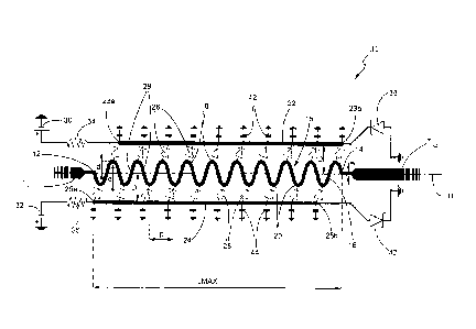
Figure 2 shows a protection device for radiocommunications
apparatuses, which is designated as a whole by 10 and which
will be referred to hereinafter as "protection device 10".
CA 02776010 2012-03-29
WO 2011/039622 PCT/IB2010/002487
9 -
The protection device 10 comprises an input terminal 12 and an
output terminal 14, connected between which is a microstrip
15, which is formed, as is known, by a ground plane 17 (Figure
3) and by a strip of conductive material, which is designated
by 16 and which will be referred to hereinafter as "path 16".
In particular, the path 16 has a width w, and is separated
from the ground plane 17 by a dielectric layer 13 having a
thickness s. The ratio w/s can be lower than one.
In detail, the path 16 lies in a plane and defines a
serpentine having pitch p. In practice, if we define a
longitudinal axis H along which the serpentine develops, the
path 16 has the shape of a portion of sinusoid with amplitude
equal to a distance d, and a period equal to the pitch p; in
addition, the path 16 defines a number n of points of maximum
18 and an equal number n of points of minimum 20. These points
of maximum and minimum 18, 20 are all at a distance d from the
longitudinal axis H, but are arranged on opposite sides with
respect to the longitudinal axis H itself. Furthermore, both
the input terminal 12 and the output terminal 14 lie along the
longitudinal axis H, arranged apart by a length LMAX.
The protection device 10 further comprises a first strip of
conductive material and a second strip of conductive material,
which are designated, respectively, by 22 and 24, and which
extend, respectively, between a first terminal 23a and a
second terminal 23b, and between a third terminal 25a and a
fourth terminal 25b. For reasons described below, hereinafter
the first and second strips of conductive material 22, 24 will
be referred to as positive virtual ground 22 and negative
virtual ground 24.
In detail, the positive virtual ground 22 and the negative
virtual ground 24 lie in the same plane in which the path 16
lies, and are arranged parallel with respect to the
CA 02776010 2012-03-29
WO 2011/039622 PCT/IB2010/002487
- 10 -
longitudinal axis H. In addition, the positive virtual ground
22 and the negative virtual ground 24 are both at a distance D
from the longitudinal axis H, and are arranged on opposite
sides with respect to the longitudinal axis H. In particular,
the positive virtual ground 22 is arranged on the same side
where the points of maximum 18 are located, whilst the
negative virtual ground 24 is arranged on the same side where
the points of minimum 20 are located. In addition, the
distance D is greater than the distance d, in such a way that
the positive virtual ground 22 and the negative virtual ground
24 are not in ohmic contact with the path 16, which is in fact
comprised between the positive virtual ground 22 and the
negative virtual ground 24.
The protection device 10 further comprises a plurality of
first diodes 26 and a plurality of second diodes 28. In
particular, in the example shown in Figure 2, the protection
device 10 comprises n first diodes 26 and n second diodes 28,
both the first diodes 26 and the second diodes 28 being, for
example, Schottky diodes.
In greater detail, each of the first diodes 26 has the
respective anode connected to a corresponding point of maximum
18 of the path 16, whilst the respective cathode is connected
to the positive virtual ground 22. In addition, each of the
second diodes 28 has its respective anode connected to the
negative virtual ground 24, whilst the respective cathode is
connected to a corresponding point of minimum 20.
In practice, the path 16 is formed by a succession of portions
of path, which will be referred to hereinafter as "connection
portions 29". Each connection portion 29 connects a respective
pair of diodes formed by a first diode 26 and by a second
diode 28 adjacent to one another, i.e., connected between a
point of maximum 18 and a consecutive point of minimum 20
along the path 16. The connection portions 29 have one and the
CA 02776010 2012-03-29
WO 2011/039622 PCT/IB2010/002487
- 11 -
same length 1; consequently, the diodes of any pair of first
diodes 26 adjacent to one another are arranged at a distance
2.1, as likewise the diodes of any pair of second diodes 28
adjacent to one another.
The protection device 10 further comprises a first voltage
generator 30 and a second voltage generator 32, and a first
pull-up resistor 34 and a second pull-up resistor 36.
In detail, the negative pole of the first voltage generator 30
is connected to ground, whilst the positive pole is connected
to a first node of the first pull-up resistor 34, the second
node of the first pull-up resistor 34 being connected to the
first terminal 23a. Instead, the positive pole of the second
voltage generator 32 is connected to ground, whilst the
negative pole is connected to a first node of the second pull-
up resistor 36, the second node of the second pull-up resistor
36 being connected to the third terminal 25a.
The protection device 10 further comprises a first transient-
voltage-suppression diode and a second transient-voltage-
suppression diode, which are also known as "transorbs" and are
designated by 38 and 40, respectively.
In greater detail, the first and second transorbs 38, 40 are
both of a unidirectional type; i.e., they behave electrically
as Zener diodes capable of conducting high currents. In
particular, the cathode of the first transorb 38 is connected
to the second terminal 23b, whilst the anode of the first
transorb 38 is connected to ground. As regards, instead, the
second transorb 40, the anode is connected to the fourth
terminal 25b, whilst the cathode is connected to ground.
The protection device 10 further comprises a plurality of
first reference capacitors 42 and a plurality of second
reference capacitors 44. In particular, in the example shown
CA 02776010 2012-03-29
WO 2011/039622 PCT/IB2010/002487
- 12 -
in Figure 2, the protection device 10 comprises n first
reference capacitors 42 and n second reference capacitors 44,
in such a way that corresponding to each between the first
reference capacitors 42 is one between the first diodes 26,
and corresponding to each between the second reference
capacitors 44 is one between the second diodes 28.
In greater detail, each of the first reference capacitors 42
is connected between ground and a corresponding point of the
positive virtual ground 22. In particular, each of the first
reference capacitors 42 is connected to the positive virtual
ground 22 in the proximity of the point in which the cathode
of the corresponding first diode 26 is connected to the
positive virtual ground 22 itself. Likewise, each of the
second reference capacitors 44 is connected between ground and
a corresponding point of the negative virtual ground 24. In
particular, each of the second reference capacitors 44 is
connected to the negative virtual ground 24 in the proximity
of the point in which the anode of the corresponding second
diode 28 is connected to the negative virtual ground 24
itself.
In order to prevent parasitic resonances, between each of the
first and second reference capacitors 42, 44 and ground there
can be connected a respective resistor (not shown), having a
resistance comprised between 0.5 0 and 1 0. Alternatively, it
is possible to use as first and second reference capacitors
42, 44 capacitors having a quality factor Q lower than two
hundred.
Operatively, the protection device 10 can be connected between
an antenna and a generic circuitry to be protected of a
radiocommunications apparatus. For example, the input terminal
12 can be connected, by means of a first transmission line Tiny
to the antenna, whilst the output terminal 14 can be
connected, by means of a second transmission line Tout, to the
CA 02776010 2012-03-29
WO 2011/039622 PCT/IB2010/002487
- 13 -
circuitry to be protected (or vice versa) The first and
second transmission lines Ti,,, Tout can have one and the same
characteristic impedance, for example 50 0, which will be
referred to hereinafter as "connection characteristic
impedance Zo". Consequently, the microstrip 15, and in
particular the path 16, function as connection between the
antenna and the circuitry to be protected.
In detail, the first voltage generator 30 and the first
transorb 38 bias the positive virtual ground 22 at a maximum
voltage Vmax, whilst the second voltage generator 32 and the
second transorb 40 bias the negative virtual ground 24 at a
minimum voltage Vmin. In particular, assuming that the first
and second transorbs 38, 40 have one and the same first
conduction voltage Vbl (also known as breakdown voltage and
understood as voltage between anode and cathode, which is
hence positive), and that the first and second voltage
generators 30, 32 generate voltages higher in magnitude than
Vbl, we have Vmax = Vbl and Vmin = -Vbl. The path 16 has
instead zero voltage.
It follows that, if the voltage of a generic point of the path
16 exceeds Vmax, for example on account of an electromagnetic
disturbance, or else because the antenna receives high-power
signals, the first diodes 26 go into conduction and are
traversed by respective currents; in addition, a current as a
whole equal to the sum of the currents that traverse the first
diodes 26 is short-circuited to ground through the first
transorb 38.
Likewise, if the voltage of a generic point of the path 16 is
lower (in magnitude and sign) than Vmin, the second diodes 28
go into conduction and are traversed by respective currents;
in addition, a current as a whole equal to the sum of the
currents that traverse the second diodes 28 is short-circuited
to ground through the second transorb 40.
CA 02776010 2012-03-29
WO 2011/039622 PCT/IB2010/002487
- 14 -
In practice, if we designate by "RF signal" in general any
electromagnetic signal that follows the path 16, it happens
that, whenever the voltage of the RF signal exceeds, in
magnitude, the first conduction voltage Vbl, the path 16 is
short-circuited to ground, alternatively through the first
diodes 26 or through the second diodes 28. Instead, in the
case where the voltage of the RF signal does not exceed, in
magnitude, the first conduction voltage Vbl, both the first
diodes 26 and the second diodes 28 are reversely biased.
In use, each diode of the first and second diodes 26, 28 can
withstand a maximum diode current Id-max. Furthermore, the
protection device 10 can be made in such a way as to have
negligible dimensions with respect to the wavelength of the
most significant spectral components of the disturbance, which
are typically negligible for frequencies higher than 60 MHz;
in fact the length LMAX can be less than 4 or 5 cm.
Consequently, it is legitimate to assume that, from the
standpoint of disturbance, the first diodes 26, as likewise
the second diodes 28, work in parallel. Hence, the protection
device 10 is capable of short-circuiting to ground a current
equal to n=Id-max, hence dissipating a power equal to n=VY=Id-max,
where VY is the threshold voltage of the first and second
diodes 26, 28. As the number of first and second diodes 26, 28
increases or decreases, the power that the protection device
10 is able to dissipate proportionally increases or decreases.
Furthermore, in the case where the disturbance is of a non-
repetitive type, i.e., having a duration of less than 2 gs and
a period of not less than 10 s, the first and second diodes
26, 28 can withstand currents up to ten times higher than the
maximum diode current Id-max, hence enabling, for this type of
disturbance, short-circuiting to ground of a current up to ten
times higher than n=Id-max=
As mentioned previously, both the first diodes 26 and the
CA 02776010 2012-03-29
WO 2011/039622 PCT/IB2010/002487
- 15 -
second diodes 28 can be Schottky diodes, which are
characterized by a high maximum diode current Id-max, a low
threshold voltage Vy, a high triggering speed, and moreover a
low parasitic capacitance Cd (lower than 0.5 pF)
Irrespective of the type of diode, the parasitic capacitance
Cd inevitably introduced by the first and second diodes 26, 28
is compensated in a distributed way by the path 16 so as to
enable use of the protection device 10 also throughout the UHF
band.
Figure 4 shows an (ideal) equivalent electrical circuit for
the path 16 and for the first and second diodes 26, 28. In
particular, it may be noted how each connection portion 29
introduces an inductance L. It may moreover be noted how the
path 16 is connected to the input terminal 12 and to the
output terminal 14 by means of a first connecting portion and
a second connecting portion, each having a length equal to
1/2, in such a way as to introduce, each of them, an
inductance equal to L/2.
In practice, the parasitic capacitance Cd of the first and
second diodes 26, 28 is compensated in a distributed way by
the inductance associated to the microstrip 15, and in
particular to the path 16, in such a way that, during
propagation along the microstrip 15, the RF signal does not
undergo any alteration, notwithstanding the presence of the
first and second diodes 26, 28. In other words, if the RF
signal is such that the voltage on the path 16 is comprised
between Vmin and Vmax, to a first approximation it propagates
along the path 16 as if the microstrip 15 were ideal, i.e., as
if the first and second diodes 26, 28 were absent.
Furthermore, from the standpoint of the RF signal, both the
first reference capacitors 42 and the second reference
capacitors 44 perform the function of supplying to the first
CA 02776010 2012-03-29
WO 2011/039622 PCT/IB2010/002487
- 16 -
diodes 26 and to the second diodes 28, respectively, a ground
reference. In other words, from the standpoint of the RF
signal that flows along the path 16, each parasitic
capacitance Cd is arranged in series with a corresponding first
reference capacitor 42 or second reference capacitor 44. Using
first and second reference capacitors 42, 44 having
capacitances higher by at least one order of magnitude than
the parasitic capacitance Cd of the first and second diodes
26, 28, we obtain that, for the RF signal, each of the
aforementioned points of maximum 18 and points of minimum 20
is connected to ground through an equivalent capacitor, which
has a capacitance approximately equal to the parasitic
capacitance Cd. Purely by way of example, assuming that the
capacitance Cd is approximately equal to 0.5 pF, each of the
first and second reference capacitors 42, 44 can have a
capacitance comprised between 10 pF and 100 pF.
Once again at a design level, the width w of the path 16, the
thickness s, and the material of the dielectric layer 13 can
be chosen in such a way that the microstrip 15 has a
characteristic impedance Z., greater than or equal to twice the
connection characteristic impedance Z, For example, if
Z0=50Q, it is possible to set Z, =12552. In this way, each
connection portion 29 approximates an inductor in a quasi-
ideal way. Furthermore, in order to compensate the parasitic
capacitances Cd introduced by the first and second diodes 26,
28, i.e., prevent the reactances introduced by them from
causing a progressive departure from Zo of the impedance of
the path 16, the inductance L can be chosen on the basis of
the following relation:
XCd + XCd -Zo
L (1)
ZFinax
where Finax is a maximum frequency at which use of the
protection device 10 is envisaged, and XCd is the reactance
CA 02776010 2012-03-29
WO 2011/039622 PCT/IB2010/002487
- 17 -
introduced by a single first diode 26 or second diode 28 at
said maximum frequency Finax, as follows:
_ 1
2)
X cd _ i 27rF' x C d
max d
As a function of the inductance L it is then possible to
determine, in a way in itself known, the geometrical
characteristics of the serpentine defined by the path 16, and
in particular the length 1 of the connection portions 29. For
example, to a first approximation the length 1 can be
determined recalling that the microstrip 15 introduces
approximately an inductance of 1 nH for each millimetre of
length, or else resorting to readily available microwave
circuit simulators.
It is moreover possible to show that, if the relations (1) and
(2) are respected, at the maximum frequency Fmax the impedance
of the path 16 is such that, proceeding from the input
terminal 12 to the output terminal 14, immediately before each
first diode 26 or second diode 28, there is an impedance Za,
whilst immediately after each first diode 26 or second diode
28, there is an impedance Zb. Furthermore, the relations
Za =Z0+JXa, Zb ZO+jXb apply, where Xa =-Xb = j=2TrFinax =L .
In practice, if Z.,_2Z0, the impedance of any point of the
path 16 is comprised between Za and Zb, and in particular lies
on a first arc of circumference Sl or on a second arc of
circumference S2 of a Smith chart, as shown in Figure 5, where
it is assumed that Z0 = 50 O.
In particular, both the first arc of circumference Si and the
second arc of circumference S2 have as extremes the impedances
(normalized with respect to Z0) Za and Zb; moreover, the first
arc of circumference Si belongs to a circumference passing
through the point of infinite impedance and through the point
CA 02776010 2012-03-29
WO 2011/039622 PCT/IB2010/002487
- 18 -
of unit normalized impedance, whilst the second arc of
circumference S2 belongs to a circumference passing through
the point of zero impedance, and through the (normalized)
points of impedance Za and Zb. In other words, given the same
inductance L, the length 1, and hence the length LMAX of the
protection device 10, is minimized with respect to the case
where the microstrip 15 has a characteristic impedance Z.<
2 Z0 .
As regards, instead, the return loss (RL) caused by the
protection device 10, it is given by
RL=10 Log Zb-Z _
Zb +Z0 (3)
Consequently, it is possible to choose the number n of first
and second diodes 26, 28 as a function of the power that it is
desired to dissipate by the protection device 10 and of a
maximum return loss.
The embodiment shown in Figure 2 can advantageously be applied
to radio-frequency receivers and transmitters, i.e., to
radiocommunications apparatuses such that the circuitry to be
protected comprises, alternatively, a receiver stage or a
transmitter stage. In fact, generally the transmitter stage
transmits to the antenna high-power signals; consequently, the
maximum voltage Vmax and the minimum voltage Vmin should
advantageously have a high magnitude to prevent the protection
device 10 from clamping these high-power signals. Instead, in
use, the receiver stage receives from the antenna low-power
signals, in such a way that the maximum voltage Vmax and the
minimum voltage Vmin can have a reduced magnitude so as to
optimize the protection afforded by the protection device 10,
without in any case clamping said low-power signals.
Purely by way of example, in the case where the circuitry to
be protected comprises just the transmitter stage, the first
CA 02776010 2012-03-29
WO 2011/039622 PCT/IB2010/002487
- 19 -
conduction voltage Vbl can be equal to 30 V. Furthermore, the
first and second voltage generators 30, 32 can supply both a
voltage equal to 33 V. Finally, the first and second pull-up
resistors 34, 36 can have a resistance equal to 10 kO.
In the case of radiocommunications apparatuses comprising both
the receiver stage and the transmitter stage, it is possible
to use the embodiment shown in Figure 6.
In particular, the protection device 10 comprises a third
transorb 46 and a fourth transorb 48. Furthermore, the
protection device 10 comprises a first transistor 50 and a
second transistor 52, a control terminal TX/RX, and a logic
inverter 54.
In detail, the third and fourth transorbs 46, 48 are both of a
unidirectional type; hence, they also behave electrically as
Zener diodes, like the first and second transorbs 38, 40. In
addition, the third and fourth transorbs 46, 48 are the same
as one another, and have one and the same second conduction
voltage Vb2, different from the first conduction voltage Vbi.
As regards, instead, the first and second transistors 50, 52,
they both perform the function of switches. In addition, the
first transistor 50 is an N-channel MOSFET, whilst the second
transistor 52 is a P-channel MOSFET.
In greater detail, the third transorb 46 has its cathode
connected to the second terminal 23b, and its anode connected
to a first conduction terminal (the distinction between source
terminal and drain terminal is not important for the purposes
of the present invention) of the first transistor 50.
Furthermore, a second conduction terminal of the first
transistor 50 and a bulk terminal of the first transistor 50
are connected to ground, whilst the gate terminal of the first
transistor 50 is connected to the control terminal TX/RX.
CA 02776010 2012-03-29
WO 2011/039622 PCT/IB2010/002487
- 20 -
The fourth transorb 48 has its anode connected to the fourth
terminal 25b, and its cathode connected to a first conduction
terminal of the second transistor 52. Furthermore, a second
conduction terminal of the second transistor 52 and a bulk
terminal of the second transistor 52 are connected to ground,
whilst the gate terminal of the second transistor 52 is
connected to an output terminal of the logic inverter 54, the
input terminal of which is connected to the control terminal
TX/RX.
Operatively, the maximum voltage Vmax and the minimum voltage
Vmin to which the positive virtual ground 22 and the negative
virtual ground 24 are biased, and in particular the magnitude
of the maximum voltage Vmax and of the minimum voltage Vmin,
are controlled by means of the control terminal TX/RX, as
described in greater detail in what follows, where it is
assumed, by way of example, that the second conduction voltage
Vb2 is lower than the first conduction voltage Vbl.
In detail, when the control terminal TX/RX assumes a logic
value "0", i.e., a value of voltage such that the first
transistor 50 is in a state of inhibition, also the second
transistor 52 is inhibited, on account of the logic inverter
54. Consequently, the first transorb 38 is connected to
ground, whilst the third transorb 46 is floating. It follows
that the maximum voltage Vmax of the positive virtual ground
22 is equal to the first conduction voltage Vbl. Furthermore,
the second transorb 46 is connected to ground, whilst the
fourth transorb 48 is floating. Consequently, the minimum
voltage Vmin of the negative virtual ground 24 is equal to -
Vbl.
Instead, when the control terminal TX/RX assumes a logic value
"1", i.e., a value of voltage such that the first transistor
50 is in a state of conduction, also the second transistor 52
is in conduction, on account of the logic inverter 54.
CA 02776010 2012-03-29
WO 2011/039622 PCT/IB2010/002487
- 21 -
Consequently, both the first and third transorbs 38, 46 are
connected to ground, as likewise the second and fourth
transorbs 40, 48. It follows that the maximum voltage Vmax of
the positive virtual ground 22 is equal to the lower voltage
between the first and second conduction voltages Vbl, Vb2; in
the case in point, on the basis of the previous assumptions,
the maximum voltage Vmax is equal to the second conduction
voltage Vb2. Likewise, the minimum voltage Vmin of the
negative virtual ground 24 is equal, in magnitude, to the
lower voltage between the first and second conduction voltages
Vbl, Vb2a; in the case in point, on the basis of the previous
assumptions, the minimum voltage Vmin is equal to -Vb2.
In practice, in the case of radiocommunications apparatuses
provided both with a transmitter stage and with a receiver
stage, it is possible to connect the embodiment shown in
Figure 6 in the way represented in Figure 7.
In particular, Figure 7 shows a radiocommunications apparatus
60, which comprises the antenna 5, the transmitter stage 2,
the receiver stage 3, and the switching stage 4. Furthermore,
the radiocommunications apparatus 60 comprises the protection
device 10, in the embodiment shown in Figure 6, which is
connected between the antenna 5 and the switching stage 4.
Operatively, assuming once again Vb2<Vbl, when the switching
stage 4 connects the transmitter stage 2 to the antenna 5, it
is possible to set on the control terminal TX/RX the logic
value "0" in such a way that the protection device 10 enters
into action only for voltages higher, in magnitude, than Vbl.
Instead, when the switching stage 4 connects the receiver
stage 3 to the antenna 5, it is possible to set on the control
terminal TX/RX the logic value "1" in such a way that the
protection device 10 enters into action already for voltages
higher, in magnitude, than Vb2. In this way, it is possible to
adapt the protection device 10 to the real needs of the
CA 02776010 2012-03-29
WO 2011/039622 PCT/IB2010/002487
- 22 -
circuitry to be protected. In fact, as mentioned previously,
it may be advantageous, when the antenna 5 is connected to the
transmitter stage 2, for the maximum voltage Vmax and the
minimum voltage Vmin to have a magnitude greater than when the
antenna 5 is connected to the receiver stage 3. This occurs
because, during normal operation of a transceiver, the
transmitter stage 2 generates signals of large amplitude,
whilst the receiver stage 3 receives signals of small
amplitude.
The advantages that the protection device 10 affords emerge
clearly from the foregoing description. In particular, the
protection device 10 enables protection of radiocommunications
apparatuses having very wide operating bands. Furthermore, the
protection device 10 entails low insertion losses and return
losses.
Finally, it is evident that modifications and variations may
be made to the protection device 10 described, without thereby
departing from the scope of the present invention, as defined
by the annexed claims.
For example, the path 16 can have a non-sinusoidal shape, but,
for example, a triangular-wave shape. Alternatively, the path
16 can also be rectilinear, even though this entails an
increase of LMAX. Furthermore, instead of the microstrip 15,
it is possible to use a coplanar line, or else another type of
transmission line for radio-frequency signals.
As regards, instead, the transorbs, it is possible to use
voltage generators in their place. Furthermore, the transorbs
can be absent, as likewise the first and second voltage
generators 30, 32 and the first and second pull-up resistors
34, 36, since both the positive virtual ground and the
negative virtual ground 22, 24 can be directly connected to
ground. In this case, the protection device 10 enters into
CA 02776010 2012-03-29
WO 2011/039622 PCT/IB2010/002487
- 23 -
action in the case where the voltage of a generic point of the
path 16 exceeds, in magnitude, the threshold voltage Vy of the
first diodes 26 and of the second diodes 28.
Finally, the connection portions 29 can have lengths different
from one another; for example, the lengths of the connection
portions 29 can be comprised in the interval 1 0.1.1.