Note: Descriptions are shown in the official language in which they were submitted.
CA 02777309 2012-05-18
243599
DEVICE FOR MEASURING ENVIRONMENTAL FORCES AND METHOD OF
FABRICATING THE SAME
BACKGROUND OF THE INVENTION
The subject matter disclosed herein relates to semiconductor
microelectromechanical
based sensors (MEMS) that can be used to detect small forces or flexures
generated from
environmental factors, for example mechanical stress, chemo-mechanical stress,
thermal
stress, electromagnetic fields, and the like. More particularly, the subject
matter
disclosed herein relates to a device for sensing pressure and a method of
fabricating the
same.
Advances in semiconductor microelectronic based sensors have served greatly to
reduce
the size and cost of such sensors. The electrical and mechanical properties of
silicon
microsensors, as well as silicon micromachining and semiconductor
microelectronic
technologies, have improved. For instance, micromachined silicon pressure
sensors,
acceleration sensors, flow sensors, humidity sensors, microphones, mechanical
oscillators, optical and RF switches and attenuators, microvalves, ink jet
print heads,
atomic force microscopy tips and the like are widely known to have found their
way into
various applications in medical, aerospace, industrial and automotive markets.
The high
yield strength, elasticity at room temperature, and hardness properties of
silicon makes it
an ideal base material for resonant structures that may, for example, be
useful for sensor
structures. Even consumer items such as watches, scuba diving equipment and
hand-held
tire pressure gauges may incorporate silicon micromachined sensors.
The demand for silicon sensors in ever expanding fields of use continues to
fuel a need
for new and different silicon microsensor geometries and configurations
optimized for
particular environments and applications. These
expanding fields of use for
1
CA 02777309 2012-05-18
243599
microelectromechanical devices in general, and sensors used to measure
environmental
forces such as pressure in particular, have created a demand for ever smaller
devices.
Unfortunately, there has been difficulty producing smaller devices that are
also highly
sensitive to small changes in pressure. Because of the small size of the
devices and the
thin nature of the geometries used, it is difficult for conventional
techniques to maintain
the stringent tolerances required, especially during high volume fabrication.
Additionally, limitations in the depth to which structures may be diffused or
implanted
within such MEMS devices during fabrication limit the design and operational
characteristics of such devices.
It would be advantageous to provide a method for manufacturing highly
sensitive
pressure sensors that are not only small in size, but which can be effectively
produced in
high volume.
The discussion above is merely provided for general background information and
is not
intended to be used as an aid in determining the scope of the claimed subject
matter.
BRIEF DESCRIPTION OF THE INVENTION
A device for measuring environmental forces, and a method for fabricating the
same, is
disclosed that comprises a device wafer, the device wafer comprising a first
device layer
separated from a second device layer by a first insulation layer. The first
device wafer is
bonded to an etched substrate wafer to create a suspended diaphragm and boss,
the
flexure of which is determined by an embedded sensing element. An advantage
that may
be realized in the practice of some embodiments of the described device and
method of
fabrication is that the thickness of both the diaphragm and the boss structure
of a MEMS
based pressure sensor can be precisely controlled using high volume planar
fabrication
techniques. In turn, these precise thicknesses determine the operational
characteristics of
the sensor, resulting in improved performance and lower positional
sensitivity, especially
in low pressure environments, for example, less than one atmosphere.
2
CA 02777309 2013-10-17
243599
In one exemplary embodiment, a device is disclosed, the device comprising a
boss
comprising a portion of a first device layer of a device wafer, the device
wafer
comprising the first device layer and a second device layer, the first device
layer
separated from the second device layer by a first insulation layer, a
diaphragm cavity
located on a top surface of a substrate wafer, the top surface of the
substrate wafer
bonded to a top surface of the first device layer to form a diaphragm over the
diaphragm
cavity, the diaphragm comprising a portion of the second device layer, and the
boss
extending from the diaphragm, and a sensing element located in the second
device layer
to sense flexure in the diaphragm.
In another exemplary embodiment, a method for fabricating a device is
disclosed
comprising the steps of forming a boss cavity on a top surface of a first
device layer of a
device wafer to form a boss, the device wafer comprising the first device
layer, a second
device layer separated from the first device layer by a first insulation
layer, and a handle
layer separated from the second device layer by a second insulation layer,
forming a
diaphragm cavity on a top surface of a substrate wafer, bonding the top
surface of the first
device layer to the top surface of the substrate wafer to form a diaphragm
over the
diaphragm cavity, the diaphragm comprising a portion of the second device
layer, and the
boss extending from the diaphragm, removing the handle layer and the second
insulation
layer from the device wafer, and placing a sensing element in the second
device layer to
sense flexure in the diaphragm.
This brief description of the invention is intended only to provide a brief
overview of
subject matter disclosed herein according to one or more illustrative
embodiments. This
brief description is provided to introduce an illustrative selection of
concepts in a
simplified form that are further described below in the detailed description.
3
CA 02777309 2013-10-17
243599
BRIEF DESCRIPTION OF THE DRAWINGS
So that the manner in which the features of the invention can be understood, a
detailed
description of the invention may be had by reference to certain embodiments,
some of
which are illustrated in the accompanying drawings. It is to be noted,
however, that the
drawings illustrate only certain embodiments of this invention and are
therefore not to be
considered limiting of its scope, for the scope of the invention encompasses
other equally
effective embodiments. The drawings are not necessarily to scale, emphasis
generally
being placed upon illustrating the features of certain embodiments of
invention. In the
drawings, like numerals are used to indicate like parts throughout the various
views.
Thus, for further understanding of the invention, reference can be made to the
following
detailed description, read in connection with the drawings in which:
FIG. I is a cross sectional view of a sensor in an exemplary embodiment of the
invention;
FIG. 2 is a process flow showing the steps in fabricating a sensor in an
exemplary
embodiment of the invention;
FIG. 3 is a cross sectional view of a device wafer having etched boss cavities
in an
exemplary embodiment of the invention; and
FIG. 4 is a cross sectional view of a device wafer having boss cavities bonded
to a
substrate wafer having a diaphragm cavity in an exemplary embodiment of the
invention.
DETAILED DESCRIPTION OF THE INVENTION
A device for measuring environmental forces, and a method for fabricating the
same, is
disclosed that comprises a device wafer, the device wafer comprising a first
device layer
separated from a second device layer by a first insulation layer. The first
device wafer is
bonded to an etched substrate wafer to create a suspended diaphragm and boss,
the
4
CA 02777309 2012-05-18
243599
flexure of which is determined by an embedded sensing element. An advantage
that may
be realized in the practice of some embodiments of the described device and
method of
fabrication is that the thickness of both the diaphragm and the boss structure
of a MEMS
based pressure sensor can be precisely controlled using high volume planar
fabrication
techniques. In turn, these precise thicknesses determine the operational
characteristics of
the sensor, resulting in improved performance and lower positional
sensitivity, especially
in low pressure environments, for example, less than one atmosphere.
An exemplary pressure sensor can be made by forming a cavity within a silicon
structure
and a diaphragm adjacent to the cavity. In absolute pressure sensor
embodiments, in
which measurements are made in relation to a selected reference pressure, the
cavity can
be held in a vacuum or a selected internal pressure. The pressure sensor
measures
pressure by sensing the flexure of the diaphragm, for example how the pressure
acting on
the diaphragm deflects the diaphragm towards or away from the diaphragm
cavity. One
or more sensing elements formed near the edges of the diaphragm typically
sense the
flexure or deflection of the diaphragm. In differential pressure sensor
embodiments, in
which pressure measurements are made with respect to the pressure acting on
the
diaphragm in relation to the environmental pressure in which the sensor is
located, the
cavity can be opened to the surrounding environment.
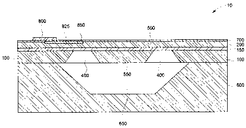
FIG. 1 shows a cross sectional view of a sensor 10 in an exemplary embodiment
of the
invention. Sensor 10 can comprise a substrate wafer 600 into which a diaphragm
cavity
650 can be etched. In one embodiment, substrate wafer 600 can be a double side
polished silicon wafer which can have n-type or p-type doping and be of a
suitable
thickness to meet the design and manufacturing requirements of the sensor 10.
In other
embodiments, substrate wafer 600 can be a device layer of a silicon-on-
insulator wafer
having an insulation layer located between a device layer and a handle layer.
Suspended
over the diaphragm cavity 650 can be a diaphragm 500, which can comprise a
portion of
a second device layer 200 and a portion of a first insulation layer 150 of a
device wafer
having two device layers separated by insulation layers, for example a double
silicon-on-
CA 02777309 2012-05-18
243599
insulator wafer (DSOI). Suspended from diaphragm 500 can be a boss 550, which
can be
a portion of a first device layer 100 of a device wafer that is separated from
the rest of the
first device layer 100 by one or more boss cavities 400.
FIG. 3 is a cross sectional view of a device wafer 50 having etched boss
cavities 400 in
an exemplary embodiment of the invention. As shown in FIG. 3, a device wafer
50 can
comprise a first device layer 100, first insulation layer 150, second device
layer 200,
second insulation layer 250, and handle layer 300. First device layer 100 can
be a single
crystal silicon substrate which, in one embodiment, can have n-type or p-type
doping and
be of a suitable thickness to meet the operational and physical design
characteristics of
the sensor 10. Second device layer 200 can be a single crystal silicon
substrate which, in
one embodiment, can be a thickness selected to meet particular design
specifications, and
which can have n-type or p-type doping. The thickness of the various layers of
the device
wafer 50 can be precisely set using conventional wafer manufacturing
techniques, and
can be selected such that the precise thickness of the layers determine the
subsequent
operational and physical characteristics of the sensor 10, as will be
described below.
First and second insulation layers 150 and 250, respectively, can, in one
exemplary
embodiment, be silicon dioxide and be of a suitable thickness to meet the
manufacturing
and design requirements of the sensor 10. Handle layer 300 can be used to grip
the
device wafer 50 during the manufacturing process. First insulator layer 150
can be
located between first device layer 100 and second device layer 200, while
second
insulation layer 250 can be located between second device layer 200 and handle
layer
300. Handle layer 300 can consist of, for example, n-type or p-type silicon
and be of a
suitable thickness to meet the design and manufacturing requirements of the
sensor 10.
Together, the thicknesses of the various layers comprising the sensor 10 can
be selected
such that the overall thickness of the device meets the operational and
physical design
characteristics of the sensor 10. In particular, the thickness of substrate
wafer 600 can be
selected to minimize packaging stress transferred to diaphragm 500.
6
CA 02777309 2012-05-18
243599
With reference again to FIG. 1, one or more sensing elements 850, for example
a
piezoresistive sensing element, can be strategically implanted or diffused
within the
second device layer 200 to sense flexure in the silicon structures caused by
environmental
forces, for example pressure, acting on sensor 10, in particular flexure of
the diaphragm
500 suspended over the open diaphragm cavity 650 within the sensor 10. Sensor
10 can
also include passivation layer 700 that can consist of, for example, a silicon
dioxide layer,
a silicon nitride layer, or a combination of both. Passivation layer 700 can
provide
electrical insulation and protection to sensor 10 during manufacturing and
operation. The
non-bonded, exterior facing side of substrate wafer 600 can also have a
passivation layer
deposited on it (not shown). One or more interconnects 825 formed in second
device
layer 200 can electrically couple one or more sensing elements 850 to an
external surface
of the sensor 10, while one or more metallization layers 800 can provide
electrical
connectivity between the interconnects 825 and an external contact on the
sensor 10 such
that the sensor 10 can be electrically coupled to other devices or connections
through, for
example, a lead attachment.
With reference to FIG. 1, an exemplary sensor 10 and operation thereof is
described in
one embodiment of the invention. Sensor 10 can operate by measuring flexure in
a
thinned structure, namely diaphragm 500, formed in second device layer 200
over a
diaphragm cavity 650 formed in the top surface of a substrate wafer 600, which
can be
bonded to the first device layer 100 of a device wafer. The diaphragm 500 can
serve as a
flexure structure in sensor 10. As the pressure differs between that in
diaphragm cavity
650 and that above diaphragm 500, diaphragm 500 will flex towards or away from
the
diaphragm cavity 650. The flexure in diaphragm 500 can be detected by one or
more
sensing elements 850 that can be placed in second device layer 200 on or near
the edges
of diaphragm 500. In one embodiment using piezoresistive sensing elements, the
resistance of sensing element 850 can be determined using a circuit, such as a
wheatstone
bridge circuit or the like, interconnected using one or more interconnects 825
attached to
one or more metallization layers 800. An electrical interface or other such
device can be
attached to the ends of the metallization layers 800 to place the sensor 10 in
electrical
7
CA 02777309 2012-05-18
243599
communication with another device. The resistance of the piezoresistive
sensing element
850 varies with the flexure of diaphragm 500. Thus, measurement of the
piezoresistive
resistance of sensing element 850 can be used to determine the amount of
flexure in
diaphragm 500, and thereby determine the pressure exerted on sensor 10.
An exemplary process for fabricating a silicon sensor such as the one
illustrated in FIG. 1
is explained with reference to FIGS. 1 through 4. FIG. 2 is an exemplary
process flow
900 for fabricating a sensor 10 in one embodiment of the invention. With
reference to
FIGS. 2 and 3, in process step 910 of FIG. 2, one or more boss cavities 400
can be etched
into first device layer 100 of a device wafer 50 to form boss 550. Boss 550
can function
as a mass attached to and extending from diaphragm 500 that concentrates
physical
stresses on the diaphragm 500 to improve pressure response and sensitivity of
the sensor.
The shape of boss 550, as determined by the one or more boss cavities 400, can
be
selected to meet design specifications. In particular, boss 550 can act to
improve the
linearity of the pressure response of sensor 10, especially in embodiments
utilizing a thin
diaphragm 500 to measure low pressure. Further the size, thickness and mass of
boss 550
can be precisely controlled based on the thickness of first device layer 100,
thereby
minimizing position sensitivity of sensor 10. Boss cavities 400 can be etched
into the
first device layer 100 down to the first insulation layer 150 using dry or wet
etching
techniques, for example DRIE, wet etching with KOH or TMAH, or other silicon
etchants or the like. First insulation layer 150 can be left in place or
etched off as well
using wet or dry removal techniques. The surface of boss cavities 400 can be,
for
example, bare silicon, oxidized silicon, doped silicon, or it can be coated
with any other
thin film capable of withstanding subsequent wafer bonding and processing
temperatures.
FIG. 4 is a cross sectional view of device wafer 50 having boss cavities 400
bonded to a
substrate wafer 600 having a diaphragm cavity 650 in an exemplary embodiment
of the
invention. With reference to FIG. 4, in process step 920 of FIG. 2, diaphragm
cavity 650
can be etched into substrate wafer 600 using dry or wet etching techniques,
for example
DRIE, wet etching with KOH or TMAH, or other silicon etchants or the like.
Diaphragm
8
CA 02777309 2012-05-18
243599
cavity 650 can have various geometries, for example square, rectangular or
circular, and
can have any required depth to meet the physical and operational design
requirements of
sensor 10, which can, in turn, depend on the design and operational
characteristics of the
sensor and/or the chosen thickness of the substrate wafer 600. The surface of
diaphragm
cavity 650 can be, for example, bare silicon, oxidized silicon, doped silicon,
or it can be
coated with any other thin film capable of withstanding subsequent wafer
bonding and
processing temperatures. In embodiments in which substrate wafer 600 comprises
the
device layer of a silicon-on-insulator wafer, the etch forming the diaphragm
cavity 650
can be chosen such that it stops at the insulation layer. Additionally, the
thickness of the
device layer of the silicon-on-insulator wafer can be precisely controlled
during
fabrication, thereby allowing the resulting thickness of substrate wafer 600
to be precisely
controlled.
With continued reference to FIG. 4, in process step 930 of FIG. 2, the top
surface of the
device wafer 50, namely the top surface of the first device layer 100 having
etched boss
cavities 400, is bonded to the top surface of substrate wafer 600, namely the
surface into
which diaphragm cavity 650 has been etched, using conventional silicon fusion
bonding
techniques. In one exemplary fusion bonding technique, the opposing surfaces
can be
made hydrophilic, that is, the surfaces can be treated with a strong oxidizing
agent that
causes water to adhere to them. The two wafers can then be placed in a high
temperature
environment to form a bond, the quality of which can be determined by the
period of time
the wafers are exposed to the high temperature environment. The silicon fusion
bonding
technique described above bonds the first device layer 100 and the substrate
wafer 600
together without the use of an intermediate adhesive material that could have
a different
coefficient of thermal expansion than the single crystal silicon wafer. The
device wafer
50 and substrate wafer 600 can be bonded such that diaphragm 500 is formed
over
diaphragm cavity 650, with boss 550 extending from diaphragm 500.
In process step 940 of FIG. 2, the handle layer 300 of device wafer 50 can be
removed
using a wet etchant, such as KOH or TMAH, which stops on the second insulation
layer
9
CA 02777309 2012-05-18
243599
250. Additionally, second insulation layer 250 can be removed using wet or dry
etching
techniques, leaving the second device layer 200 exposed. In other embodiments,
both the
handle layer 300 and the second insulation layer 250 can be removed and/or
thinned
using physical thinning techniques such as grinding.
In process step 950 of FIG. 2, and with reference again to FIG. 1, passivation
layer 700
can be deposited on the exposed top surface of second device layer 200 using,
for
example, silicon dioxide, silicon nitride layers, or combinations of both. As
part of
process step 950, the non-bonded, exterior facing side of substrate wafer 600
can also
have a passivation layer deposited on it (not shown). In process step 960 of
FIG. 2, one
or more sensing elements 850 can be placed in the second device layer 200 by
diffusion
or ion implantation of, in one embodiment using piezoresistive sensing
elements, low
doped p-type material into a doped n-type second device layer 200 in a
predefined
position relative to the diaphragm 500, which can be formed as part of the
second device
layer 200. For example, Boron implantation and diffusion at high temperature
may form
piezoresistive sensing elements 850 within second device layer 200. The
sensing
elements 850 can be positioned to sense flexure in diaphragm 500. It should be
noted
that any number of sensing elements 850 may be employed and their exact
positioning
relative to the diaphragm 500 may be different depending on the particular
application,
expected pressures, sensitivity requirements, and the like. Additionally, one
or more
interconnects 825 can be added by diffusion or ion implanting of, for example,
highly
doped p-type material into a doped n-type second device layer 200.
Interconnect 825 can
provide electrical conductivity to the sensing element 850, and can be placed
in an
overlapping configuration with sensing element 850. The components diffused or
implanted in process step 960 can be performed using a single process or
separately
implanted or diffused using multiple processes
Next, in process step 970, metallization layer 800 can be added, providing
electrical
conductivity from the outer surface of sensor 10 to sensing element 850
through
interconnect 825. To provide access to interconnect 825, openings can be made
in
CA 02777309 2012-05-18
243599
passivation layer 700 using dry or wet etching techniques. Metallization layer
800 can
then be added and formed of, for example, gold or aluminum, and can be created
to a
desired thickness to suit device design and fabrication requirements.
As shown in FIG. 1, sensor 10 could be configured to provide absolute pressure
measurements in relation to the reference pressure established within
diaphragm cavity
650. If, however, a differential pressure sensor is desired, diaphragm cavity
650 can be
made to extend entirely through substrate wafer 600 by removing or thinning a
portion of
the bottom surface of substrate wafer 600 using DRIE, wet etching with KOH or
TMAH,
or other silicon etchants or the like. In some embodiments, the bottom portion
of
substrate wafer 600 could be removed and/or thinned using physical thinning
techniques
such as grinding. In embodiments in which substrate wafer 600 comprises a
silicon-on-
insulator wafer, the handle layer and insulation layer of the silicon-on-
insulator wafer can
be removed, with additional thinning of the device layer performed as
required. In still
further embodiments, a passivation layer could be added to the bottom of the
substrate
wafer 600 following the thinning process.
With reference to the embodiments described herein, each etch made during the
fabrication of sensor 10 can have any chosen geometry and can have any
required depth
depending on the particular application. The selected depth and geometry of
each etch
can be selected to alter the design characteristics of the resulting sensor
10. Additionally,
the thickness of second device layer 200 and the size and shape of the
diaphragm 500
dictated by diaphragm cavity 650 can be selected to determine the sensitivity
of the
resulting sensor 10. The selected thickness of second device layer 200, which
can be
arbitrarily chosen and precisely controlled in manufacturing the device
wafers, leads to
improved control over the flexibility of diaphragm 500, and therefore improved
control
over the performance characteristics of the resulting sensor 10. Similarly,
the thickness
of first device layer 100 can determine the thickness, mass and operating
characteristics
of the boss 550 more precisely than when using traditional etching and/or
implanting
techniques. Additionally, the planar manufacturing processes are ideal for
manufacturing
11
CA 02777309 2013-10-17
243599
purposes and can increase not only the fabrication yield, but the overall
reliability and
long term performance of the resulting devices. Accordingly, uniform control
over the
performance characteristics of the sensor 10 can be achieved.
The above detailed description is provided to illustrate exemplary embodiments
and is
not intended to be limiting. Although the method for fabricating a sensor has
been shown
and described with respect to embodiments which measure pressure, it will be
apparent to
those skilled in the art that similar techniques can be used to fabricate
sensors capable of
measuring other parameters. For example, it should be recognized that the
apparatus and
method of manufacture described herein are useful in a wide variety of other
applications
not explicitly described herein. It will also be apparent to those skilled in
the art that
numerous modifications and variations within the scope of the present
invention are
possible. Further, numerous other materials and processes can be used within
the scope
of the exemplary methods and structures described as will be recognized by
those skilled
in the art. For example, it should be recognized that the p-type and n-type
materials
described herein can be used in an alternative fashion, e.g., by replacing p-
type materials
for n-type materials and vice versa. Additionally, it will be apparent to
those of skill in
the art that the sequence of steps identified and described in various
exemplary
embodiments need not occur in the sequence described, and that in other
embodiments
various steps can be combined, performed in different orders, either
contiguously, non-
contiguously, or in parallel, and still achieve the same result.
This written description uses examples to disclose the invention, including
the best mode,
and also to enable any person skilled in the art to practice the invention,
including making
and using any devices or systems and performing any incorporated methods. The
patentable scope of the invention is defined by the claims, and may include
other
examples that occur to those skilled in the art in view of the description.
12