Note: Descriptions are shown in the official language in which they were submitted.
CA 02777603 2012-04-13
WO 2010/046105 PCT/EP2009/007563
1 Description
2 Electrochemical sensor and method for the production thereof
3 The invention relates to an electrochemical sensor, in
4 particular for the detection and/or quantification of
chemical substances or materials in extremely small
6 quantities or concentrations. It furthermore relates to a
7 method for producing a sensor of this type.
8 Highly sensitive sensors for detecting even extremely small
9 quantities or concentrations of selected chemical substances
can be used in a large number of applications. Sensors of
11 this type can advantageously be used in particular in the
12 measurement of extremely small quantities of chemical and
13 biochemical substances, such as gases or biomolecules, e.g.
14 in the following fields:
= environmental protection, in the measurement of air quality
16 and water quality
17 = military and homeland protection, in the detection of toxic
18 or explosive substances
19 = chromatography
= use as "artificial noses" in quality assurance, e.g. in the
21 foodstuffs, beverages or perfume industry
22 The invention is based on the object of specifying a sensor,
23 in particular an electrochemical sensor, with which even
24 extremely small quantities or concentrations of a chemical
target substance can be detected or quantified with high
26 accuracy in a particularly reliable manner. Furthermore, the
27 intention is to specify a particularly suitable method for
28 producing a sensor of this type.
29 With regard to the sensor, this object is achieved according
to the invention with a detector zone, the electrical
31 conductivity of which is determined by electronic tunneling,
32 ionization or hopping processes, in particular between
CA 02777603 2012-04-13
WO 2010/046105 PCT/EP2009/007563
2 -
1 localized states or nanoparticles, and the electrochemical
2 interaction thereof with a target substance to be detected.
3 In this case, the invention is based on the consideration
4 that the sensor should expediently be oriented toward an
electrical or electronic measurement principle with regard to
6 the measurement values or signals yielded exhibiting
7 utilizability and further processability that are as
8 expedient as possible. In order in this case to provide the
9 particularly high sensitivity desired with regard to the
presence of particles of the chemical target substance,
11 therefore, a sensor parameter that is particularly readily
12 accessible from a metrological standpoint, that is to say, in
13 particular, the conductivity or electrical resistance of said
14 sensor, should be predetermined in such a way that the sensor
reacts even to extremely small changes in the number of
16 particles or concentration of the chemical target substance
17 in its vicinity very sensitively with a comparatively greatly
18 pronounced change in its electrical conductivity or its
19 electrical resistance.
This can be achieved by providing a system in a detector zone
21 wherein, by means of electrically insulated nanoparticles,
22 dopings, defects or traps or by means of structural disorder,
23 localized states or a zero-dimensional electron gas or energy
24 states trapped in some other way are formed for charge
carriers. Charge transport can then take place only in
26 thermally activated fashion upon the supply of an assisting
27 external electrical, electromagnetic or thermal activation
28 energy. Possible conduction mechanisms are: the so-called
29 hopping mechanism, field emission or ionization effect,
Poole-Frenkel effect or a differently configured tunnel
31 effect of the electrons between the localized sites or
32 defects or traps. This is because precisely in the case of
33 systems of this type, wherein the electron transport is based
34 substantially on tunnel, ionization or hopping effects, the
CA 02777603 2012-04-13
WO 2010/046105 PCT/EP2009/007563
3 -
1 electrical conductivity is extremely dependent on the
2 electrical coupling of the individual localized states to one
3 another.
4 This in turn is dependent, given suitable configuration of
the other system parameters such as, for example, material
6 choice, geometry parameters, average distance between the
7 localized states and the like, very sensitively on the
8 electrochemical interaction with the target substance, such
9 that even in the case of extremely small changes in the
concentration or quantity of particles of the target
11 substance in the vicinity of the detector zone, comparatively
12 large effects on the electrical conductivity are obtainable,
13 particularly since the electrical parameters such as
14 resistance or conductivity in the case of systems of this
type change exponentially with the coupling strength between
16 the tunneling partners, which coupling strength can be
17 influenced by said interaction.
18 In this case, the electrochemical interaction of said
19 tunneling or hopping processes with the target substance to
be detected can be effected directly, in particular by
21 contact between the carrier medium loaded with the target
22 substance and the detector zone or indirectly, that is to say
23 across certain short distances. In particular, in this case,
24 as a result of contact or interaction of the target substance
present in the gaseous or liquid phase with the detector zone
26 of the sensor, an exchange of electrons or ions or else an
27 electrostatic or electromagnetic interaction between the
28 sensor and the target substance can take place, which alters
29 the electron concentration or the electron mobility in the
material of the detector zone and/or, in particular, the
31 coupling between the nanoparticles. Thus, even inherently
32 electrically neutral substances such as water, for example,
33 can be detectable since dipole moments can also disturb the
34 local electron concentration in the detector zone.
CA 02777603 2012-04-13
WO 2010/046105 PCT/EP2009/007563
- 4 -
1 In the case of the dominance of hopping processes for the
2 electrical conductivity a(T) of the detector zone, which
3 occurs in generally disordered, structureless systems such as
4 amorphous silicon, for example, for said detector zone the
temperature dependence of its electrical conductivity is
6 preferably given approximately by the relation In c - T-1. In
7 this case, the detector zone is advantageously configured in
8 such a way that the characteristic exponent y of this
9 relationship has a value of between 0 and 1, preferably
approximately the value 0.25, approximately the value 0.5 or
11 approximately the value 1.
12 Advantageously, the detector zone is formed from
13 nanoparticles embedded into a matrix, said nanoparticles
14 having a higher electrical conductivity in comparison with
the matrix material.
16 In order to ensure the intended dominance of the electronic
17 tunneling, ionization or hopping processes for the electrical
18 conductivity of the detector zone, the material forming the
19 latter advantageously has a particularly suitable morphology.
In particular, the morphology in the detector zone is in this
21 case preferably chosen in such a way that a multiplicity of
22 zones having a comparatively small extent and having a
23 comparatively high electrical conductivity are formed, which
24 adjoin one another or are connected to one another via
intermediate zones having a comparatively low electrical
26 conductivity. For this purpose, the material forming the
27 detector zone could have an amorphous, nano- or
28 polycrystalline structure, for example. Advantageously,
29 however, the detector zone is formed from nanoparticles
embedded into a matrix composed of suitably selected, in
31 particular non-conductive, material having a comparatively
32 low electrical conductivity, said nanoparticles having a
33 higher electrical conductivity in comparison with the matrix
CA 02777603 2012-04-13
WO 2010/046105 PCT/EP2009/007563
-
1 material. Such locally changing zones having low and high
2 conductivity are thus formed, for example, by composite
3 systems composed of conductive nanocrysta=llites, defects or
4 traps or dopings embedded in an electrically insulating
5 matrix (base medium). Such systems characterized by a
6 nanocrystalline construction are also designated as
7 nanocomposites.
8 In this case, the nanoparticles can be formed from material
9 having a suitably high electrical conductivity, for example
from semiconducting or superconducting material. However, a
11 setting of desired properties that is particularly compliant
12 with requirements can be achieved by means of the
13 nanoparticles advantageously being formed in metallic
14 fashion, in particular from gold (Au), tungsten or platinum
(P1) .
16 Preferably, inorganic, organic or dielectric material or else
17 polymer material is provided for forming the matrix.
18 Advantageously, the material forming the detector zone, said
19 material being provided as sensor-active material, is
designed, with regard to the choice of its respective
21 parameters, especially with a view to the desired great
22 dependence of the electrical conductivity on the interaction
23 with the target substance. In order to ensure this, in
24 particular, the nanoparticles or the defects that bring about
the localized states are selected, with regard to their size,
26 distances, constitution and number density of particles upon
27 embedding into the matrix, in a targeted manner and
28 selectively with regard to the possible interaction with the
29 target substance.
Moreover, said parameters are advantageously chosen suitably
31 in such a way that the resulting electrical conductivity is
32 substantially dominated by said electronic tunneling,
CA 02777603 2012-04-13
WO 2010/046105 PCT/EP2009/007563
- 6 -
1 ionization or hopping processes. In this case, the
2 nanoparticles have, for example, an average particle size of
3 up to 10 nm, preferably of up to 1 nm. Alternatively,
4 however, particle sizes of up to 100 nm or more are also
conceivable, provided that they are sufficiently electrically
6 insulated from one another and their distances are
7 sufficiently small, such that tunnel effects can be
8 established between them. When setting the particle size, it
9 is advantageously taken into account that, precisely when
using the nanocomposites, the comparatively small particles,
11 in comparison with larger particles, have a larger specific
12 (internal) surface area, that is to say surface area in
13 relation to the volume, such that they have a particularly
14 high energetic reactivity with the target substance.
Therefore, in principle, a sensor having a rough,
16 nanocrystalline surface is more sensitive to an
17 electrochemical reaction than a sensor having a smooth
18 surface.
19 In one advantageous development, the detector zone is formed
by a coating applied to a carrier body or a substrate.
21 Since the sensor is constructed on the basis of
22 nanocomposites in its detector zone, it can be embodied in
23 laterally very small dimensionings with recourse to
24 particularly suitable production or deposition methods. As a
result, the sensor, and in particular the detector zone
26 thereof, in the manner of a nanosensor, can be positioned
27 with pinpoint accuracy and in a manner compliant with
28 requirements at an intended location - which, for example, is
29 particularly suitable for the detection of the respective
target substance - on a larger structure, for example a
31 larger substrate. This also makes it possible, in particular,
32 to equip a substrate with a comparatively complex system with
33 different types of sensor functionalities. Thus, by way of
34 example, in a simple manner, it is possible to provide a
CA 02777603 2012-04-13
WO 2010/046105 PCT/EP2009/007563
- 7 -
1 microarray or microgrid of nanosensors that are different in
2 terms of equipment, size and/or design for interaction with
3 target substances, each nanosensor advantageously being
4 designed in each case for the detection of a specific type of
chemical substance. Thus, in the manner of parallel detection
6 or processing, mixed states of different chemicals or
7 substances can also be detected in a single, simultaneous
8 measurement step, which would otherwise have to be analyzed
9 sequentially in a time-consuming manner. For the purposes
mentioned, in a particularly advantageous configuration in a
11 particularly advantageous configuration, a plurality of
12 detector zones that differ from one another with regard to
13 the material choice for the matrix and/or the nanoparticles
14 and/or the size and/or density of the nanoparticles are
arranged on a common carrier body.
16 In principle, various technologies are conceivable for
17 producing the sensor and, in particular, the detector zone.
18 However, one method which can be adapted particularly well to
19 the design principles of the sensor, in particular to the
provision of the detector zone, and is thus particularly
21 suitable for production and with which the object in this
22 regard is achieved according to the invention is deposition
23 by local energy excitation, such as, for example, ion beam-
24 induced, pyrolytically induced or photon beam-induced
deposition, particularly advantageously electron beam-induced
26 deposition (EBID). In this case, "local energy excitation"
27 should be understood to mean, in particular, that the lateral
28 extent of the depositions arising as a result of the energy
29 excitation is significantly smaller, for example a few nm to
a few pm, than the dimensions of the substrate, of a few
31 100 pm or a few mm, for example, that is used for the
32 deposition. The methods mentioned are based on the physical
33 and chemical transformation processes taking place under a
34 scanned particle beam, consisting of electrons, ions or
photons, or a beam of electromagnetic waves, in a precursor
CA 02777603 2012-04-13
WO 2010/046105 PCT/EP2009/007563
- 8 -
1 gas present at the beam location. This method enables,
2 particularly with the aim of deposit structuring on a
3 microscopic scale, a targeted material deposition of
4 functional nanostructures, in which case, through the choice
of suitable deposition parameters, a targeted spatial
6 construction of the desired structures is possible in a
7 manner limited to the spatial composition desired in the end
8 product.
9 This means that a subsequent aftertreatment of structures
once they have been deposited, in accordance with
11 conventional methods such as, for example, by means of
12 lithographic etching or the like, is not necessary to produce
13 the desired spatial form in the miniaturized end product. In
14 particular, specific silicon and mask techniques or
semiconductor-based carrier substrates or a clean room
16 environment are/is no longer required. In this case, the
17 deposit structuring process is based on the principle that
18 molecules of a starting structural substance (precursor)
19 which are in the gas phase and adsorb on a surface within a
vacuum environment are excited by means of a locally
21 concentrated incidence of energy, which can consist, for
22 example, of focused electrons, ions or photons or other
23 energetically concentrated objects, and are fixed by means of
24 a decomposition or conversion process of their bonds as a
sediment or deposit permanently on a surface of a substrate
26 situated in the vicinity. In this case, the initial material
27 deposit simultaneously serves as a seed for new deposits that
28 are guided by the local position of the energy action and the
29 residence duration thereof, such that any desired three-
dimensional objects can be deposited on the substrate,
31 depending on the focusability of the energy source with up to
32 nanometer precision accuracy.
33 Through the suitable choice of the starting substances or
34 precursor materials and also through the suitable choice of
CA 02777603 2012-04-13
WO 2010/046105 PCT/EP2009/007563
9 -
1 the parameters used during the deposition process, in this
2 case it is possible to influence the microscopic properties
3 of the end product in a particularly flexible and far-
4 reaching manner. In particular, it is possible to set both
the size of the nanocrystallites and their distances and
6 starting materials during the production process by means of
7 the ambient parameters such as, for example, beam
8 acceleration voltage, beam current, precursor material, etc.,
9 such that specific, targeted sensor materials coordinated
with the interaction with a predeterminable target substance
11 and having high selectivity relative to the respective target
12 substance can be produced.
13 In order to ensure, in the detector zone, the desired great
14 dependence of the electrical conductivity on the
abovementioned interaction and the targeted and comparatively
16 homogeneous distribution of nanoparticles in a suitable
17 matrix, as provided for this purpose, in this case organic,
18 inorganic, dielectric or organometallic complexes, monomers,
19 oligomers, polymers or mixtures of said monomers, oligomers
and polymers, which are preferably in the gas phase and have
21 a vapor pressure that is particularly expedient for
22 deposition, are advantageously used as precursor materials.
23 Advantageously, in particular CH3, C502H7, C502F3H4, C502F6H,
24 C5H5, Me2Au (acac) [empirical formula: (CH3) 2AuC5O2H7] ,
Me2Au(tfac) [empirical formula: (CH3) 2AuC502F3H4] , Me3Au(hfac)
26 [empirical formula: (CH3) 2AuC5O2F6H] , Cu (hfac) 2 [empirical
27 formula: Cu (C502F6H) 2] , CpPtMe3 (empirical formula:
28 C5H5Pt (CH3) 3] , CpMePtMe3 [empirical formula: C5H4 (CH3) Pt (CH3) 3] ,
29 MO(CO)6' W(CO)6, WF6, [RhCl (PF3) 2] 2, C02(CO)8, AuCl(PF3) and/or
Ni(CO)4r are/is used as precursor substance.
31 The abovementioned deposition method is suitable, in
32 particular, both for producing a surface coating for
33 producing the detector zone on a substrate serving as carrier
34 body in the manner of subsequent refinement of the carrier
CA 02777603 2012-04-13
WO 2010/046105 PCT/EP2009/007563
- 10 -
1 body, and for producing a bulk body, wherein the base body of
2 the sensor per se is already formed from the nanoparticles
3 embedded into the matrix and thus forms in turn in its
4 totality the detector zone. In order to produce such
structures, advantageously an energetic particle beam
6 provided for the energetic excitation of the precursor
7 substances or a local pyrolytic treatment, for example by
8 means of a laser beam, is guided, with respect to the
9 substrate, laterally or three-dimensionally depending on a
predetermined desired geometry of the deposit. In this case,
11 in particular, a plurality of respectively mutually different
12 detector zones for forming a complex sensor system can be
13 deposited on a common substrate or carrier body.
14 Advantageously, the temperature of the substrate is regulated
suitably during the deposition. This influences the speed of
16 the surface diffusion processes on the substrate, which leads
17 to a regulable subsequent supply rate of precursor material
18 and thus to a controlled growth rate of the deposit.
19 Alternatively, the subsequent supply rate can also be
regulated by the temperature of the precursor source being
21 increased or decreased, since this directly influences the
22 vapor pressure of the precursor.
23 Alternatively, the pyrolytic or pyrolytically induced
24 deposition can advantageously be used as well. In this case,
solid deposits can also be deposited on a substrate by means
26 of the substrate being heated after nondirectional adsorption
27 of precursor molecules, for example from below by means of a
28 heating wire or from above by means of a laser beam. The
29 supply of energy then locally effects the desired conversion
of the precursor materials.
31 By means of the application of the abovementioned deposit
32 structuring, in particular by means of the production of the
33 detector zone or else of the entire base body of the sensor
CA 02777603 2012-04-13
WO 2010/046105 PCT/EP2009/007563
- 11 -
1 by means of electron beam-induced deposition or else by means
2 of ion beam-induced, pyrolytically induced or photon beam-
3 induced deposition, it is possible to achieve a particularly
4 high flexibility in the setting of desired properties of the
end product. In particular, through the choice of a suitable
6 structure for the matrix, not only is it possible to suitably
7 set the electrical conductivity with the aim of the desired
8 sensitivity in the event of a change in the interaction with
9 the environment, rather a targeted influencing of the
production parameters during the deposition of the structures
11 also enables a targeted influencing of other microscopic
12 properties.
13 The advantages achieved by means of the invention consist, in
14 particular, in the fact that by virtue of the provision of a
detector zone on the basis of nanoparticles embedded into a
16 matrix, it is possible to achieve a particularly sensitive
17 dependence of the electrical conductivity of the detector
18 zone on changes in the ambient conditions of the sensor, in
19 particular the particle density of the selected target
substance, on an extremely small scale. Particularly
21 sensitive measurements associated with extremely small
22 changes in the quantity of the target substance can thus be
23 carried out. The local concentration of the target substance
24 can thus be measured particularly precisely, such that it is
possible to provide highly accurate sensors on the basis of
26 such measurements. The dependence of the electrical
27 conductivity primarily on the coupling of the nanoparticles
28 among one another also ensures, in particular, that the
29 interaction with the particles of the target substance that
are situated in the environment, by means of direct contact
31 or else indirectly by means of electrical or magnetic
32 interaction, results directly in a particularly sensitive
33 dependence of the conductivity on the quantity or
34 concentration of particles in the environment of the sensor.
A particularly sensitive detection of particles of the target
CA 02777603 2012-04-13
WO 2010/046105 PCT/EP2009/007563
- 12 -
1 substance and also the quantitative determination thereof are
2 thus possible, in which case even inherently electrically
3 neutral substances such as water, for example, can also be
4 detectable on account of their dipole moment.
Sensors of this type can advantageously be used for example
6 in the measurement of extremely small quantities of chemical
7 and biochemical substances, such as gases or biomolecules,
8 e.g. in the following fields:
9 = environmental protection, in the measurement of air quality
and water quality
11 = military and homeland protection, in the detection of toxic
12 or explosive substances
13 = chromatography
14 = use as "artificial noses" in quality assurance, e.g. in the
foodstuffs, beverages or perfume industry
16 By means of the production of the detector zone or else of
17 the entire sensor by means of deposit structuring methods
18 such as, in particular, electron beam-induced deposition, the
19 targeted production of microscopic structures with a high
bandwidth of desired properties is additionally possible, in
21 which case, in particular by means of suitable material and
22 parameter selections, the electrical properties can be set
23 particularly expediently and in a targeted manner and
24 selectively with respect to the target substance chosen. In
particular, the use of electron beam-induced deposition makes
26 it possible to produce extremely miniaturized sensors or
27 sensor elements, in which case, in particular, the detection
28 geometry is virtually freely selectable.
29 An exemplary embodiment of the invention is explained in
greater detail with reference to a drawing, in which:
31 FIG. 1 shows a miniaturized electrochemical sensor,
32
CA 02777603 2012-04-13
WO 2010/046105 PCT/EP2009/007563
- 13 -
1 FIG. 2 shows a deposit growing on a substrate,
2 FIG. 3 shows a measuring arrangement comprising a sensor
3 according to FIG. 1,
4 FIG. 4 shows a diagram with a number of energy levels, and
FIG. 5 shows the sensor according to FIG. 1 with a
6 plurality of detector zones.
7 Identical parts are provided with the same reference symbols
8 in all the figures.
9 The miniaturized sensor 1 in accordance with FIG. 1 is
provided, in particular, for use as an electrochemical sensor
11 for the detection and/or quantification of chemical materials
12 or substances even in extremely small quantities or
13 concentrations. Alternatively, however, a large number of
14 further application possibilities in microsensor technology
or biosensor technology or the like are also conceivable. The
16 miniaturized sensor 1 comprises a substrate or a base body 4,
17 which is provided with a detector zone 10, which is in turn
18 formed by preferably metallic nanoparticles 14 embedded in a
19 matrix 12. In this case, in the exemplary embodiment, the
matrix 12 is configured as a polymer matrix into which the
21 metallic nanoparticles 14 are embedded. In this case, the
22 nanoparticles 14 form embedded localized states for
23 electrical charges. Alternatively or additionally, these can
24 also be formed by defects or traps or by structural disorder,
for example in an amorphous medium.
26 However, the nanocrystals are not absolutely necessary for
27 the sensor effect per se. They are advantageous in the
28 operation of the sensor, however, since they additionally
29 intensifies the sensor effect. This is achieved by virtue of
the fact that the crystallites can be constructed with the
CA 02777603 2012-04-13
WO 2010/046105 PCT/EP2009/007563
- 14 -
1 aid of the proposed production method in such a way that they
2 have diameters of the order of magnitude of 1 nanometer or
3 less. These particles have a particularly increased ratio of
4 surface area to volume. Therefore, on account of their
microscopic roughness relative to the target substance to be
6 detected they have a higher energetic reactivity or an
7 increased effective sensor surface area relative to
8 homogeneous bulk bodies having a smooth surface. External
9 influences on the electrical conduction mechanisms, such as
on the hopping or tunneling conductivity, are thereby
11 promoted or intensified, and the electrochemical sensor
12 effect is likewise intensified overall.
13 With regard to the material choice of matrix 12 and
14 nanoparticles 14 and also with regard to the average particle
size of approximately 1 nm in the exemplary embodiment and
16 the density of the nanoparticles 14, the corresponding
17 parameters are chosen in such a way that the electrical
18 transport between the nanoparticles 14 within the matrix 12
19 is characterized by hopping processes and is guided by means
of tunneling processes. Therefore, the conduction mechanism
21 in the detector zone 10 is effected by means of the thermally
22 activated hopping mechanism (hopping, nearest neighbor
23 hopping, variable range hopping) between localized sites and
24 arises as a result of a quantum mechanical tunnel effect.
Complying with these boundary conditions ensures that the
26 electrical conductivity of the detector zone 10 is very
27 greatly and sensitively also dependent on the coupling
28 between the nanoparticles 14 and thus on the electromagnetic
29 environment of the sensor 1, such that this is detectable
with high sensitivity and resolution.
31 In this case, the sensor 1 in accordance with FIG. 1 is
32 constructed with recourse to a substrate of conventional
33 design based on silicon, said substrate serving as a carrier
34 body 16 and being provided with a superficial coating in
CA 02777603 2012-04-13
WO 2010/046105 PCT/EP2009/007563
- 15 -
1 order to form the detector zone 10. The design of the sensor
2 1 according to FIG. 1 thus corresponds to a refinement of a
3 conventional substrate, wherein the detector zone 10 provided
4 for the high measurement resolution desired is applied by a
subsequent coating.
6 Since the deposition methods proposed for sensor production,
7 such as electron beam-induced deposition, do not necessarily
8 rely on silicon as a substrate support, the sensor, besides
9 on silicon, can practically also be deposited on any other
solid support desired. Consequently, the deposition method
11 proposed is suitable, in a particularly flexible manner, for
12 subsequently equipping or refining different materials,
13 surfaces or already prefabricated or existing structures with
14 sensor functionality.
As an example, a "lab-on-a-chip" application shall be
16 mentioned here which can have e.g. a large number of flow
17 channels or measurement chambers for gases and liquids. Such
18 lab-on-a-chip arrangements are usually prefabricated using
19 silicon mask technology. The proposed method for the
production of an electrochemical sensor would allow such a
21 chip subsequently to be equipped with sensor functionality at
22 any desired location.
23 The detector zone 10 of the sensor 1 and possibly also the
24 entire base body 4 are produced by so-called deposit
structuring, wherein particular growth of the respective
26 structures is produced in and also restricted to those
27 spatial regions in which the arising of the desired
28 structures is provided. The subsequent, for example
29 lithographic, etching required in the case of other
miniaturized structures is thus obviated. In the exemplary
31 embodiment, the method of so-called electron beam-induced or
32 ion beam-induced deposition is provided for producing the
33 respective structures. In this case, a phase in which the
CA 02777603 2012-04-13
WO 2010/046105 PCT/EP2009/007563
- 16 -
1 corresponding structures arise is illustrated in FIG. 2.
2 As can be gathered from the schematic illustration in FIG. 2,
3 in a suitable environment, in particular in a vacuum,
4 precursor substances, as illustrated in FIG. 2 on the basis
of particles 50, are introduced in gaseous form into the
6 vicinity of a substrate 52. As a result of adhesion forces
7 between the precursor molecules and substrate, an adsorption
8 of precursor material takes place on the substrate.
9 In a deposition zone 54 in direct proximity to the substrate
52, the precursor substances are energetically excited to
11 conversion, in which case the conversion products deposit in
12 solid and nonvolatile form as a sediment or deposit 56
13 permanently on the substrate 52. In this case, the initial
14 material deposit on the substrate 52 simultaneously serves as
a seed for new deposits that are guided by the local position
16 of the energy effect and the residence duration thereof, such
17 that virtually any desired three-dimensional objects can be
18 produced on the substrate 52. In this case, the excitation
19 for conversion and thus for deposition is effected by local
energy excitation or application, an electron beam 58 being
21 provided for this purpose in the exemplary embodiment. In
22 terms of its lateral extent, said electron beam is
23 significantly smaller than the surface of the substrate 52,
24 such that the energy excitation actually takes place only
locally and in a manner delimited to a comparatively small
26 proportion of the substrate surface.
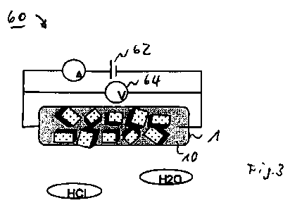
27 A measuring arrangement 60 comprising the sensor 1 is shown
28 schematically in FIG. 3. In this case, the detector zone 10
29 of the sensor 1 is electrically connected to a current source
62, which can be embodied as a constant-current source, in
31 particular. By means of a voltage sensor 64, the voltage V
32 present across the detector zone 10 in the case of a
33 predetermined current flow can be tapped off, such that the
CA 02777603 2012-04-13
WO 2010/046105 PCT/EP2009/007563
- 17 -
1 electrical resistance or the electrical conductivity of the
2 detector zone 10 can be measured by means of this
3 arrangement. This changes on account of the specific
4 configuration of the detector zone 10 owing to its
electrochemical interaction with a target substance to be
6 detected in its environment, for example water (H20),
7 hydrochloric acid (HC1) or the like.
8 In this case, the type of reaction of the detector zone 10 to
9 the presence of the target substance is illustrated
schematically in the energy diagram in accordance with FIG.
11 4. In this energy diagram, a location characteristic value is
12 plotted on the x-axis and an energy value E is plotted on the
13 y-axis. Localized electronic states characterized by their
14 corresponding energy levels 70, 72, 74, 76, 78, as plotted in
FIG. 4, are situated in the detector zone 10. In the example
16 according to FIG. 4, the energy levels 70, 72, 74 in this
17 case represent localized energy states between which an
18 electron changes places by means of a thermally activated
19 hopping mechanism. In this case, the example according to
FIG. 4 illustrates by way of example such a hopping process
21 between the energy levels 72 and 74, which, for example, can
22 also be assigned to two adjacent nanocrystallites 14.
23 Given the presence of a target substance to be detected, for
24 example the chemical HC1, in the environment of the detector
zone 10, the energetic distance between two adjacent
26 localized energy states 76, 78 can be increased by the
27 magnitude tE by means of electrical or electrochemical
28 interaction with the target substance. Here the electron e
29 would then have to surmount a greater energy magnitude,
compared with the unchanged energy levels (such as, for
31 example, the energy levels 72, 74), in order to change places
32 assigned to the energy levels 76, 78. Thus, the electron
33 mobility is reduced by the increase in energetic distance
34 between said energy levels or the electrical resistance of
CA 02777603 2012-04-13
WO 2010/046105 PCT/EP2009/007563
- 18 -
1 the detector zone 10 is increased. Through the material
2 choice in the detector zones 10 and also the concentration of
3 the localized energy states, it is possible to effect an
4 individualized adaptation of the detector zone 10 to an
intended target substance and the interaction with the
6 latter. This enables an individualized orientation of the
7 reaction of the detector zone 10 to the presence of a desired
8 target substance in the immediate environment.
9 The exemplary embodiment according to FIG. 5 illustrates a
sensor 1, wherein a plurality of detector zones 10 are
11 arranged on a common carrier body 16. Said detector zones are
12 in each case connected independently of one another to
13 suitable current sources 62 and voltage sensors 64, such that
14 their respective electrical resistance or their respective
electrical conductivity can be measured independently of the
16 others. Thus, a spatially resolved detection of the intended
17 target substance is possible by virtue of a suitable spatial
18 arrangement of the detector zones 10 relative to one another.
19 Additionally or alternatively, the detector zones 10 can
differ from one another with regard to the material choice of
21 the matrix and/or the nanoparticles or their other
22 microscopic properties and can thus be adapted to different
23 target substances with regard to their interaction with the
24 environment. Thus, with comparatively simple means, it is
possible to provide a comparatively complex system with
26 different sensor functionalities in the manner of a
27 microarray or microgrid. Thus, in the manner of parallel
28 detection or processing, mixed states of different chemicals
29 or the like can also be detected in a single, simultaneous
measurement step.
CA 02777603 2012-04-13
WO 2010/046105 PCT/EP2009/007563
- 19 -
List of reference symbols
1 Sensor
4 Base body
Detector zone
12 Matrix
14 Nanoparticles
16 Carrier body
50 Particles
52 Substrate
54 Deposition zone
56 Deposit
Y Exponent
0 Conductivity