Note: Descriptions are shown in the official language in which they were submitted.
110014: 910020
CA 02777675 2012-04-13
DESCRIPTION
TITLE OF INVENTION
Silicon Carbide Semiconductor Device and Method of Manufacturing Thereof
TECHNICAL FIELD
The present invention relates to a silicon carbide semiconductor device and a
method of manufacturing thereof, and particularly to a silicon carbide
semiconductor
device exhibiting excellent electrical characteristics and a method of
manufacturing
thereof.
BACKGROUND ART
Conventionally, silicon carbide semiconductor devices in which silicon carbide
(SiC) is used have been known, and an example of them is disclosed in
W0011018872
(hereinafter "PTL V) for example. PTL 1 discloses a MOS-type field effect
transistor
(MOSFET) that is formed as a silicon carbide semiconductor device using an SiC
substrate of the 4H polytype having a surface orientation of substantially {03-
38}.
According to PTL 1 disclosing the MOSFET, a gate oxide film is formed by dry
oxidation and a high channel mobility (about 100 cm2/Vs) can be achieved.
CITATION LIST
PATENT LITERATURE
PTL 1: WO01/018872
SUMMARY OF INVENTION
TECHNICAL PROBLEM
In order for a silicon carbide semiconductor device in which SiC is used to
stably exhibit its excellent electrical characteristics, it is required to
achieve a high
channel mobility with high reproducibility.
The inventors of the present invention have conducted studies to found,
however, that even the MOSFET disclosed in PTL 1 may not have a sufficiently
high
channel mobility depending on the case.
-1-
CA 02777675 2012-04-13 110014:910020
In view of the circumstances above, an object of the present invention is to
provide a silicon carbide semiconductor device capable of achieving a high
channel
mobility with high reproducibility, and a method'of manufacturing the same.
SOLUTION TO PROBLEM
The present invention is a silicon carbide semiconductor device including a
semiconductor layer made of silicon carbide and having a surface tilted at an
angle in a
range of not less than 50 and not more than 65 relative to a (00011 plane,
and an
insulating film formed to contact the surface of the semiconductor layer, a
maximum
value of a nitrogen concentration in a region within 10 nm from an interface
between
the semiconductor layer and the insulating film is not less than lx 1021 CM-3
, and the
silicon carbide semiconductor device has a channel direction in a range of 10
relative
to a direction orthogonal to a <-2110> direction in the surface of the
semiconductor
layer.
Further, the present invention is a silicon carbide semiconductor device
including: a substrate made of silicon carbide of a first conductive type; a
semiconductor layer made of silicon carbide of the first conductive type,
formed on a
surface of the substrate, containing a first-conductive-type impurity of a
lower
concentration than the substrate, and having a surface tilted at an angle in a
range of not
less than 50 and not more than 65 relative to a 100011 plane; a second-
conductive-
type impurity diffusion layer formed in the surface of the semiconductor
layer; a first-
conductive-type impurity diffusion layer formed in a surface of the second-
conductive-
type impurity diffusion layer; an insulating film formed to contact the
surface of the
semiconductor layer; a source electrode formed to contact at least a part of a
region,
except for a portion where the insulating film is formed, of the surface of
the
semiconductor layer; a gate electrode formed on the insulating film; and a
drain
electrode formed on a surface of the substrate opposite to the surface of the
substrate on
which the semiconductor layer is formed. A maximum value of a nitrogen
concentration in a region within 10 nm from an interface between the
semiconductor
-2-
CA 02777675 2012-04-13 110014:910020
layer and the insulating film is not less than 1 x 10²¹ CM-3 , and the silicon
carbide
semiconductor device has a channel direction in a range of 10 relative to a
direction
orthogonal to a <-2110> direction in the surface of the semiconductor layer.
Further, the present invention is a silicon carbide semiconductor device
including: a substrate made of silicon carbide of a first conductive type; a
semiconductor layer made of silicon carbide of the first conductive type,
formed on the
substrate, containing a first-conductive-type impurity of a lower
concentration than the
substrate, and having a surface tilted at an angle in a range of not less than
50 and not
more than 65 relative to a (00011 plane; a second-conductive-type impurity
diffusion
layer formed in the surface of the semiconductor layer; a first-conductive-
type impurity
diffusion layer formed in a surface of the second-conductive-type impurity
diffusion
layer; an insulating film formed to contact the surface of the semiconductor
layer; a
source electrode formed to contact a part of a region, except for a portion
where the
insulating film is formed, of the surface of the semiconductor layer; a drain
electrode
formed to contact another part of the region, except for the portion where the
insulating
film is formed, of the surface of the semiconductor layer; and a gate
electrode formed
on the insulating film. A maximum value of a nitrogen concentration in a
region
within 10 nm from an interface between the semiconductor layer and the
insulating film
is not less than 1 x 10²¹ CM-3 , and the silicon carbide semiconductor device
has a channel
direction in a range of 10 relative to a direction orthogonal to a <-2110>
direction in
the surface of the semiconductor layer.
Here, in the silicon carbide semiconductor device of the present invention,
preferably the source electrode has a surface in a stripe pattern.
Further, in the silicon carbide semiconductor device of the present invention,
preferably the source electrode has a surface in a honeycomb pattern.
Further, in the silicon carbide semiconductor device of the present invention,
preferably the surface of the semiconductor layer is a crystal plane tilted at
an angle in a
range of 5 relative to a {03-38} plane.
-3-
CA 02777675 2012-04-13 110014:910020
Furthermore, the present invention is a method of manufacturing a silicon
carbide semiconductor device, including the steps of: forming a semiconductor
layer
made of silicon carbide and having a surface tilted at an angle in a range of
not less than
50 and not more than 65 relative to a {0001) plane; inspecting a direction
orthogonal
to a <-2110> direction in the surface of the semiconductor layer; forming an
insulating
film contacting a part of the surface of the semiconductor layer so that a
channel
direction is set in a range of 10 relative to the direction orthogonal to
the <-2110>
direction in the surface of the semiconductor layer; and adjusting a nitrogen
concentration so that a maximum value of the nitrogen concentration in a
region within
10 nm from an interface between the semiconductor layer and the insulating
film is not
less than 1 x 1021 cm 3.
Here, regarding the method of manufacturing a silicon carbide semiconductor
device of the present invention, preferably the direction orthogonal to the <-
2110>
direction in the surface of the semiconductor layer is inspected based on an
orientation
of a defect included in the semiconductor layer.
Further, regarding the method of manufacturing a silicon carbide semiconductor
device of the present invention, preferably the step of adjusting the nitrogen
concentration includes the step of performing a heat treatment in an
atmosphere of a gas
containing nitrogen, on the semiconductor layer where the insulating film is
formed.
Further, regarding the method of manufacturing a silicon carbide semiconductor
device of the present invention, preferably the step of adjusting the nitrogen
concentration includes the step of performing, on the semiconductor layer
having
undergone the heat treatment, a heat treatment in an atmosphere of an inert
gas.
ADVANTAGEOUS EFFECTS OF INVENTION
The present invention can provide a silicon carbide semiconductor device that
can achieve a high channel mobility with high reproducibility, as well as a
method of
manufacturing the same.
BRIEF DESCRIPTION OF DRAWINGS
-4-
CA 02777675 2012-04-13 110014:910020
Fig. 1 is a schematic cross section of an example of a vertical DiMOSFET that
is an example of the silicon carbide semiconductor device of the present
invention.
Fig. 2 is a schematic plan view of the silicon carbide semiconductor device
shown in Fig. 1 as seen from a gate electrode side.
Fig. 3 is a schematic cross section illustrating a part of a manufacturing
process
of an example of the method of manufacturing a silicon carbide semiconductor
device
of the present invention.
Fig. 4 is a schematic perspective view illustrating a part of the
manufacturing
process of an example of the method of manufacturing a silicon carbide
semiconductor
device of the present invention.
Fig. 5 is a schematic cross section of an example of the substrate used for
the
present invention.
Fig. 6 is a schematic cross section illustrating a part of the manufacturing
process of an example of the method of manufacturing a silicon carbide
semiconductor
device of the present invention.
Fig. 7 is a schematic plan view of an example of a surface of a semiconductor
layer used for the present invention.
Fig. 8 is a schematic cross section illustrating a part of the manufacturing
process of an example of the method of manufacturing a silicon carbide
semiconductor
device of the present invention.
Fig. 9 is a schematic cross section illustrating a part of the manufacturing
process of an example of the method of manufacturing a silicon carbide
semiconductor
device of the present invention.
Fig. 10 is a schematic cross section illustrating a part of the manufacturing
process of an example of the method of manufacturing a silicon carbide
semiconductor
device of the present invention.
Fig. 11 is a schematic cross section illustrating a part of the manufacturing
process of an example of the method of manufacturing a silicon carbide
semiconductor
-5-
CA 02777675 2012-04-13 110014:910020
device of the present invention.
Fig. 12 is a schematic plan view illustrating a part of the manufacturing
process
of an example of the method of manufacturing a silicon carbide semiconductor
device
of the present invention.
Fig. 13 is a schematic plan view of another example of the silicon carbide
semiconductor device of the present invention as seen from a gate electrode
side.
Fig. 14 is a diagram showing an example of a nitrogen concentration
distribution in the vicinity of the interface between an insulating film and a
semiconductor layer in an example of the silicon carbide semiconductor device
of the
present invention.
Fig. 15 is a diagram showing an example of the relation between an angle ( )
relative to the <-2110> direction and a channel mobility (relative value) in a
surface of
a semiconductor layer in an example of the silicon carbide semiconductor
device of the
present invention.
Fig. 16 is a schematic cross section of an example of a lateral MOSFET that is
an example of the silicon carbide semiconductor device of the present
invention.
Fig. 17 is a schematic plan view of the silicon carbide semiconductor device
shown in Fig. 16 as seen from a gate electrode side.
Fig. 18 is a schematic cross section illustrating a part of a manufacturing
process
of an example of the method of manufacturing a silicon carbide semiconductor
device
of the present invention.
Fig. 19 is a schematic cross section illustrating a part of the manufacturing
process of an example of the method of manufacturing a silicon carbide
semiconductor
device of the present invention.
Fig. 20 is a schematic cross section illustrating a part of the manufacturing
process of an example of the method of manufacturing a silicon carbide
semiconductor
device of the present invention.
Fig. 21 is a schematic cross section illustrating a part of the manufacturing
-6-
CA 02777675 2012-04-13 110014:910020
process of an example of the method of manufacturing a silicon carbide
semiconductor
device of the present invention.
DESCRIPTION OF EMBODIMENTS
Embodiments of the present invention will hereinafter be described. In the
drawings of the present invention, the same reference characters denote the
same or
corresponding parts.
Where crystal plane and direction are to be expressed, they should actually be
expressed with a bar on a required number. Because of restricted expression
means,
however, they are expressed in the present invention with "-" added before a
required
number instead of a bar on the required number. Further, in the present
invention, an
individual orientation is denoted in [], a group orientation is denoted in o,
an
individual plane is denoted in (), and a group plane is denoted in {}.
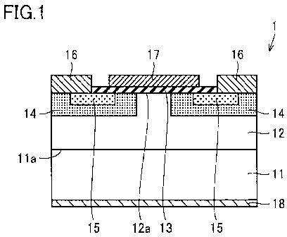
<First Embodiment>
Fig. 1 shows a schematic cross section of an example of a vertical DiMOSFET
(Double Implanted Metal Oxide Semiconductor Field Effect Transistor) that is
an
example of the silicon carbide semiconductor device of the present invention.
A silicon carbide semiconductor device 1 shown in Fig. 1 includes a substrate
11 made of silicon carbide of n type and 4H-SiC polytype for example, a
semiconductor
layer 12 made of silicon carbide of n type formed on a surface 11 a of
substrate 11, a
second-conductive-type impurity diffusion layer 14 that is a p-type region
formed in a
surface 12a of semiconductor layer 12, a first-conductive-type impurity
diffusion layer
15 that is an n-type region formed in a surface of second-conductive-type
impurity
diffusion layer 14 (also in surface 12a of semiconductor layer 12), an
insulating film 13
formed to contact surface 12a of semiconductor layer 12, a source electrode 16
formed
in a region of surface 12a of semiconductor layer 12 other than a region where
insulating film 13 is formed, a gate electrode 17 formed on a surface of
insulating film
13, and a drain electrode 18 formed on the back surface of substrate 11.
Here, surface 11 a of substrate 11 on which semiconductor layer 12 is formed
is
-7-
CA 02777675 2012-04-13 110014:910020
a crystal plane tilted at an angle in a range of not less than 50 and not
more than 65
relative to the {0001 } plane.
Further, as semiconductor layer 12, a layer such as a layer made of silicon
carbide of n type having a lower n-type impurity concentration than substrate
11 for
example may be used. Surface 12a of semiconductor layer 12 is also a crystal
plane
tilted at an angle in a range of not less than 50 and not more than 65
relative to the
{0001 } plane.
Further, as insulating film 13, a film such as an oxide film formed for
example
by dry oxidation (thermal oxidation) or the like may be used. Insulating film
13 is not
limited to a single-layer structure, and may be of a structure including two
or more
layers.
Further, as second-conductive-type impurity diffusion layer 14, a layer such
as a
p-type region may be used that is formed by diffusing a p-type impurity
serving as a
second-conductive-type impurity in surface 12a of semiconductor layer 12, for
example.
Here, as the p-type impurity serving as a second-conductive-type impurity,
aluminum,
boron, or the like may be used, for example. Furthermore, in at least a part
of a region
excluding the region where first-conductive-type impurity diffusion layer 15
is formed
in the surface of second-conductive-type impurity diffusion layer 14, a p+-
type region
containing a p-type impurity serving as a second-conductive-type impurity and
having a
higher concentration than second-conductive-type impurity diffusion layer 14
may be
formed.
Further, as first-conductive-type impurity diffusion layer 15, a layer such as
an
n-type region that is formed by diffusing an n-type impurity serving as a
first-
conductive-type impurity in surface 12a of semiconductor layer 12 may be used,
for
example. The concentration of the n-type impurity as the first-conductive-type
impurity in first-conductive-type impurity diffusion layer 15 may be made
higher than
the concentration of the n-type impurity as the first-conductive-type impurity
in
semiconductor layer 12. Here, as the n-type impurity serving as a first-
conductive-
-8-
CA 02777675 2012-04-13 110014:910020
type impurity, nitrogen, phosphorous or the like may be used, for example.
Further, for source electrode 16, gate electrode 17, and drain electrode 18
each,
a conventionally known metal or the like may be used, for example.
In silicon carbide semiconductor device 1 shown in Fig. 1, a maximum value of
the nitrogen concentration in a region within 10 nm from the interface between
semiconductor layer 12 and insulating film 13 is not less than 1 x 10²¹ CM-3 .
Here, the
region within 10 nm from the interface between semiconductor layer 12 and
insulating
film 13 refers to a region made up of. a region extending from the interface
between
semiconductor layer 12 and insulating film 13 perpendicularly to the interface
toward
semiconductor layer 12 side by 10 nm; and a region extending from the
interface
between semiconductor layer 12 and insulating film 13 perpendicularly to the
interface
toward insulating film 13 side by 10 nm.
Fig. 2 shows a schematic plan view of silicon carbide semiconductor device I
shown in Fig. 1 as seen from gate electrode 17 side. Here, the surface of
source
electrode 16 and the surface of gate electrode 17 are formed to extend in a
stripe pattern
in the <-2110> direction and, along the direction which is perpendicular to
the
<-2110> direction, source electrode 16 and gate electrode 17 are alternately
arranged.
One gate electrode 17 is disposed between two source electrodes 16. From a gap
between source electrode 16 and gate electrode 17, a surface of insulating
film 13 is
exposed. Thus, where the surface of source electrode 16 has the stripe
pattern, the
channel direction tends to be set easily in a range of 10 relative to the
direction
orthogonal to the <-2110> direction, in surface 12a of semiconductor layer 12
as will
be described later herein. In the present invention, the channel direction
means the
direction in which carriers move in surface 12a of semiconductor layer 12.
Here, the channel direction of silicon carbide semiconductor device 1 with the
above-described structure is set to be included in a range of 10 relative to
the
direction orthogonal to the <-2110> direction, in surface 12a of semiconductor
layer 12.
In the following, a description will be given of an example of the method of
-9-
CA 02777675 2012-04-13 110014:910020
manufacturing silicon carbide semiconductor device 1 having the above-
described
structure. First, as shown in a schematic cross section of Fig. 3, substrate
11 made of
silicon carbide (4H-SiC) having surface 11a formed of a crystal plane that is
tilted at an
angle in a range of not less than 50 and not more than 65 relative to the
(00011 plane
is prepared.
Here, substrate 11 having surface 11 a as described above may be formed for
example as shown in a schematic perspective view of Fig. 4, by slicing an n-
type silicon
carbide crystal ingot 10 which is a crystal grown in the [0001] direction (c-
axis
direction) to have an exposed {0001 } plane, along the direction at an angle a
in a
range of not less than 50 and not more than 65 relative to the {0001) plane,
so that a
crystal plane (hatched portion in Fig. 4) that is tilted at an angle in a
range of not less
than 50 and not more than 65 relative to the {0001 } plane is exposed, for
example.
Further, it is preferable that surface 11 a of substrate 11 that is tilted at
an angle
in a range of not less than 50 and not more than 65 relative to the {0001 }
plane is also
a crystal plane tilted at an angle in a range of 5 relative to a {03-38}
plane as shown
for example in a schematic cross section of Fig. 5. In the case where surface
11 a of
substrate 11 is a crystal plane tilted at an angle in a range of 5 relative
to the {03-38}
plane, electrical characteristics such as channel mobility of silicon carbide
semiconductor device 1 tend to be improved. In order to further improve
electrical
characteristics such as channel mobility of silicon carbide semiconductor
device 1,
preferably surface II a of substrate 11 is a crystal plane tilted at an angle
in a range of
3 relative to the {03-38} plane, and most preferably surface l la of
substrate 11 is the
{03-38} plane. As is evident, a crystal plane tilted at an angle in a range of
5
relative to the {03-38} plane and a crystal plane tilted at an angle in a
range of 3
relative to the {03-38} plane each include the {03-38} plane.
Next, as shown in a schematic cross section of Fig. 6, semiconductor layer 12
is
formed on surface 11 a of substrate 11.
Here, semiconductor layer 12 may be formed for example by epitaxial growth or
-10-
CA 02777675 2012-04-13 110014:910020
the like of semiconductor layer 12 made of n-type silicon carbide having an n-
type
impurity with a lower concentration than substrate 11, on surface 11 a of
substrate 11.
Where semiconductor layer 12 is formed by the above-described epitaxial
growth,
surface 12a of semiconductor layer 12 is allowed to have the same crystal
plane as
surface 11 a of substrate 11. Therefore, surface 12a of semiconductor layer 12
can be a
crystal plane tilted at an angle in a range of not less than 50 and not more
than 65
relative to the {0001 } plane.
Further, for a similar reason to the above-described one, surface 12a of
semiconductor layer 12 is preferably a crystal plane tilted at an angle in a
range of 5
relative to the {03-38 } plane, more preferably a crystal plane tilted at an
angle in a
range of 3 relative to the {03-38} plane, and most preferably the (03-38)
plane.
As is also evident here, a crystal plane tilted at an angle in a range of 5
relative to the
{03-38} plane and a crystal plane tilted at an angle in a range of 3
relative to the
{03-38} plane each include the {03-38} plane.
Next, as shown in a schematic plan view of Fig. 7, the direction orthogonal to
the <-2110> direction in surface 12a of semiconductor layer 12 is inspected.
Here, the direction orthogonal to the <-2110> direction in surface 12a of
semiconductor layer 12 can be inspected based on a defect included in
semiconductor
layer 12 for example. Specifically, since a defect may be formed at a certain
site of
semiconductor layer 12 in a process of manufacturing silicon carbide
semiconductor
device 1, the direction orthogonal to the <-2110> direction in surface 12a of
semiconductor layer 12 can be identified relative to the position of the
defect formed at
a certain site of semiconductor layer 12. Further, the direction orthogonal to
the
<-2110> direction in surface 12a of semiconductor layer 12 can also be
identified
based on the surface morphology of semiconductor layer 12.
Next, as shown in a schematic cross section of Fig. 8, second-conductive-type
impurity diffusion layer 14 is formed in surface 12a of semiconductor layer
12. In this
example, second-conductive-type impurity diffusion layer 14 is formed in a
stripe
-11-
CA 02777675 2012-04-13 110014:910020
pattern extending in the <-2110> direction. Second-conductive-type impurity
diffusion layer 14, however, is not limited to this form.
Here, second-conductive-type impurity diffusion layer 14 may be formed for
example by ion implantation or the like in which ions of a p-type impurity
serving as a
second-conductive-type impurity are implanted into surface 12a of
semiconductor layer
12, after an ion implantation block mask is placed in a region other than the
region
where second-conductive-type impurity diffusion layer 14 is to be formed in
surface
12a of semiconductor layer 12. As the ion implantation block mask, an oxide
film or
the like that has been patterned by photolithography and etching for example
may be
used.
Next, as shown in a schematic cross section of Fig. 9, first-conductive-type
impurity diffusion layer 15 is formed in a surface of second-conductive-type
impurity
diffusion layer 14 formed in the above-described manner. In this example,
first-
conductive-type impurity diffusion layer 15 is also formed in a stripe pattern
extending
in the <-2110> direction. First-conductive-type impurity diffusion layer 15,
however,
is not limited to this form.
Here, first-conductive-type impurity diffusion layer 15 may be formed for
example by ion implantation or the like in which ions of an n-type impurity
serving as a
first-conductive-type impurity are implanted into surface 12a of semiconductor
layer 12,
after an ion implantation block mask is placed in a region other than the
region where
first-conductive-type impurity diffusion layer 15 is to be formed in surface
12a of
semiconductor layer 12. As the ion implantation block mask, an oxide film or
the like
that has been patterned by photolithography and etching for example may be
used as
well.
Next, an activation annealing treatment is performed on semiconductor layer 12
in which second-conductive-type impurity diffusion layer 14 and first-
conductive-type
impurity diffusion layer 15 have been formed in the above-described manner.
Accordingly, the p-type impurity serving as a second-conductive-type impurity
in
-12-
CA 02777675 2012-04-13 110014:910020
second-conductive-type impurity diffusion layer 14 as well as the n-type
impurity
serving as a first-conductive-type impurity in first-conductive-type impurity
diffusion
layer 15 that have been introduced by the above-described ion implantation can
be
activated.
Here, the activation annealing treatment may be performed for example in an
argon gas atmosphere by heating semiconductor layer 12 in which second-
conductive-
type impurity diffusion layer 14 and first-conductive-type impurity diffusion
layer 15
have been formed, at a temperature of approximately 1700 C for approximately
30
minutes, for example.
Next, as shown in a schematic cross section of Fig. 10, insulating film 13 is
formed to contact the whole of surface 12a of semiconductor layer 12 after
second-
conductive-type impurity diffusion layer 14 and first-conductive-type impurity
diffusion
layer 15 have been formed therein.
Here, as insulating film 13, an oxide film or the like formed for example by
dry
oxidation (thermal oxidation) or the like may be used. Dry oxidation (thermal
oxidation) may be performed for example in air or oxygen by heating surface
12a of
semiconductor layer 12 in which second-conductive-type impurity diffusion
layer 14
and first-conductive-type impurity diffusion layer 15 have been formed in the
above-
described manner, at a temperature of approximately 1200 C for approximately
30
minutes for example.
Next, a nitrogen annealing treatment is performed on semiconductor layer 12 on
which above-described insulating film 13 has been formed. In this way, the
nitrogen
concentration is adjusted so that a maximum value of the nitrogen
concentration in a
region within 10 nm from the interface between semiconductor layer 12 and
insulating
film 13 is not less than 1 x 1021 cm 3.
Here, in the above-described nitrogen annealing treatment, semiconductor layer
12 on which above-described insulating film 13 has been formed is heated for
example
in an atmosphere of a gas containing nitrogen such as nitrogen monoxide (NO)
gas at a
-13-
CA 02777675 2012-04-13 110014:910020
temperature of approximately 1100 C for approximately 120 minutes for example.
In
this way, a maximum value of the nitrogen concentration in the region within
10 nm
from the interface between semiconductor layer 12 and insulating film 13 can
be set to
1x1021 cm -3 or more.
It is preferable to further perform an inert gas annealing treatment on
semiconductor layer 12 having undergone the above-described nitrogen annealing
treatment, in an atmosphere of an inert gas such as argon gas for example. In
the case
where the above-described inert gas annealing treatment is performed on
semiconductor
layer 12 having undergone the above-described nitrogen annealing treatment,
there is a
higher tendency for silicon carbide semiconductor device 1 to be able to
achieve a high
channel mobility with high reproducibility.
Here, the above-described inert gas annealing treatment may be performed for
example in an argon gas atmosphere by heating semiconductor layer 12 having
undergone the above-described nitrogen annealing treatment, at a temperature
of
approximately 1100 C for approximately 60 minutes for example.
Next, as shown in a schematic cross section of Fig. 11, a part of insulating
film
13 formed as described above is removed to pattern insulating film 13.
Here, patterning of insulating film 13 is performed for example as shown in a
schematic plan view of Fig. 12, so that the channel direction is included
within a range
of 10 relative to the direction orthogonal to the <-2110> direction in
surface 12a of
semiconductor layer 12. Namely, patterning of insulating film 13 is performed
so that
the channel direction is parallel to any direction within a range from -10
relative to the
direction orthogonal to the <-2110> direction to +10 relative to the
direction
orthogonal to the <-2110> direction, in surface 12a of semiconductor layer 12.
Further, a part of insulating film 13 may be removed for example by forming,
on the surface of insulating film 13, an etching mask patterned by means of
photolithography and etching for exposing a part to be removed of insulating
film 13,
for example, and thereafter etching and thereby removing the exposed part of
insulating
-14-
CA 02777675 2012-04-13 110014:910020
film 13.
Next, as shown in Fig. 1, source electrode 16 is formed to contact the exposed
surface of first-conductive-type impurity diffusion layer 15 in surface 12a of
semiconductor layer 12 that is exposed from the part where insulating film 13
has been
removed.
Here, source electrode 16 may be formed for example by performing sputtering
for example to form an electrically conductive film made of a metal such as
nickel for
example, on surface 12a of semiconductor layer 12 exposed after the above-
described
etching of insulating film 13 and on the surface of the above-described
etching mask,
and thereafter removing this etching mask. In other words, the conductive film
formed on the surface of the etching mask is removed (lifted off) together
with the
etching mask while only the conductive film formed on surface 12a of
semiconductor
layer 12 is left to serve as source electrode 16.
Preferably, a heat treatment for achieving alloying is performed on
semiconductor layer 12 on which above-described source electrode 16 has been
formed.
Here, the heat treatment for achieving alloying may be performed for example
in an atmosphere of an inert gas such as argon gas by heating semiconductor
layer 12
on which above-described source electrode 16 has been formed, at a temperature
of
approximately 950 C for approximately two minutes for example.
Next, as shown in Fig. 1, gate electrode 17 is formed on a surface of
insulating
film 13. Here, gate electrode 17 may be formed for example by performing
photolithography and etching or the like to form a resist mask having an
opening
corresponding to a portion where gate electrode 17 is to be formed and
covering
respective entire surfaces of insulating film 13 and source electrode 16, then
performing
for example sputtering or the like to form an electrically conductive film
made of a
metal such as aluminum for example, on the surface of the resist mask and on
the
surface of insulating film 13 that is exposed from the opening of the resist
mask, and
thereafter removing this resist mask. In other words, the conductive film
formed on
- 15 -
CA 02777675 2012-04-13 110014:910020
the surface of the resist mask is removed (lifted off) together with the
resist mask while
only the conductive film formed on the surface of insulating film 13 is left
to serve as
gate electrode 17.
Next, as shown in Fig. 1, drain electrode 18 is formed on the back surface of
substrate 11. Here, drain electrode 18 may be formed for example by performing
for
example sputtering or the like to form an electrically conductive film made of
a metal
such as nickel for example, on the back surface of substrate 11.
In this way, silicon carbide semiconductor device 1 with the structure shown
in
Fig. 1 can be manufactured.
In silicon carbide semiconductor device 1 of the present invention, the
surface
of source electrode 16 may be formed in a honeycomb pattern and a region
except for a
partial region surrounding the outer periphery of source electrode 16 may be
formed as
gate electrode 17 as shown for example in a schematic plan view of Fig. 13.
In the case where the surface of source electrode 16 is formed in a honeycomb
pattern as described above, the surface of each source electrode 16 is formed
in the
shape of a hexagon. In particular, the surface of source electrode 16 is
preferably
formed in the shape of a regular hexagon. In the case where each source
electrode 16
has its surface formed in the shape of a regular hexagon, setting of the
channel direction
within a range of 10 relative to the direction orthogonal to the <-2110>
direction is
facilitated, and the number of silicon carbide semiconductor devices 1 that
can be
formed from substrate 11 of the same size can be increased. Therefore, there
is a
tendency that silicon carbide semiconductor device 1 having a high channel
mobility
can be fabricated with higher reproducibility and at a higher manufacturing
efficiency.
Other features of silicon carbide semiconductor device 1 having source
electrode 16 and gate electrode 17 structured as shown in Fig. 13 may be
similar to the
above-described ones.
In silicon carbide semiconductor device 1 structured in the above-described
manner, when a negative voltage is applied to source electrode 16 and a
positive
-16-
CA 02777675 2012-04-13 110014:910020
voltage is applied to gate electrode 17 and drain electrode 18 for example,
carriers
(electrons in the above-described example) injected from source electrode 16
move to
drain electrode 18 through the surface of first-conductive-type impurity
diffusion layer
15, the surface of second-conductive-type impurity diffusion layer 14, the
inside of
semiconductor layer 12, and the inside of substrate 11.
If a negative voltage is applied to source electrode 16 and a positive voltage
is
applied to drain electrode 18 while the positive voltage is not applied to
gate electrode
17, carriers (electrons in the above-described example) injected from source
electrode
16 can be restricted in movement in the surface of second-conductive-type
impurity
diffusion layer 14.
In silicon carbide semiconductor device 1 having the above-described
structure,
on surface 11 a of substrate 11 tilted at an angle in a range of not less than
50 and not
more than 65 relative to the {0001 } plane of n-type silicon carbide (4H-SiC)
for
example, semiconductor layer 12 made of n-type silicon carbide containing an n-
type
impurity as the first-conductive-type impurity with a lower concentration than
substrate
11 can be formed by epitaxial growth. In the case of this structure, surface
12a
(crystal plane tilted at an angle in a range of not less than 50 and not more
than 65
relative to the {0001 } plane) of semiconductor layer 12 can be used for a
channel in
which carriers move. Therefore, as compared with the case where the {0001 }
plane is
used for the channel, a higher carrier mobility (channel mobility) can be
achieved.
Further, in silicon carbide semiconductor device 1 having the above-described
structure, a maximum value of the nitrogen concentration in a region within 10
nm
from the interface between semiconductor layer 12 and insulating film 13 is
not less
than 1 x 10²¹ CM -3 as shown for example in Fig. 14. Therefore, in silicon
carbide
semiconductor device 1 of the present invention, the number of interface
states that
occur when insulating film 13 is formed by dry oxidation (thermal oxidation)
or the like
at the interface between semiconductor layer 12 and insulating film 13 can be
reduced.
Accordingly, particularly in a channel directly below insulating film 13 (the
channel is
-17-
CA 02777675 2012-04-13 110014:910020
located on the surface portions of second-conductive-type impurity diffusion
layer 14
between first-conductive-type impurity diffusion layer 15 and semiconductor
layer 12,
which are also surface 12a of semiconductor layer 12 that contacts insulating
film 13),
the carrier mobility (channel mobility) can stably be improved.
Fig. 14 shows an example of the nitrogen concentration distribution in the
vicinity of the interface between insulating film 13 and semiconductor layer
12 in
silicon carbide semiconductor device 1 with the above-described structure.
Here, in
Fig. 14, the vertical axis represents the nitrogen concentration (cm-3 ) and
the horizontal
axis represents the distance (nm) from the interface between insulating film
13 and
semiconductor layer 12. Further, in Fig. 14, the portion where the distance
(nm) on
the horizontal axis is 0 (nm) represents the interface between insulating film
13 and
semiconductor layer 12. The extension in the leftward direction with respect
to the
portion of 0 (nm) on the horizontal axis of the distance (nm) represents
extension in the
direction toward insulating film 13 side, while the extension in the rightward
direction
with respect to the portion of 0 (nm) on the horizontal axis of the distance
(nm)
represents extension in the direction toward semiconductor layer 12 side.
Further, silicon carbide semiconductor device 1 with the above-described
structure has the channel direction in a range of 10 relative to the
direction
orthogonal to the <-2110> direction in surface 12a of semiconductor layer 12.
Carriers therefore move smoothly in this channel direction, and the carrier
mobility in
this channel direction and electric current characteristics can be improved.
Accordingly, the ON resistance of silicon carbide semiconductor device 1 can
be
reduced.
Fig. 15 shows an example of the relation between the channel mobility
(relative
value) and the angle ( ) relative to the <-2110> direction in surface 12a (in
the crystal
plane tilted at an angle in a range of not less than 50 and not more than 65
relative to
the {0001 } plane) of semiconductor layer 12 of silicon carbide semiconductor
device 1
with the above-described structure. In Fig. 15, the vertical axis represents
the channel
-18-
CA 02777675 2012-04-13 110014:910020
mobility (relative value) and the horizontal axis represents the angle ( )
relative to the
<-2110> direction in surface 12a of semiconductor layer 12. As to the angle (
) on
the horizontal axis in Fig. 15, the angle is not distinguished in terms of the
direction of
tilt relative to the <-2110> direction. Therefore, 80 on the horizontal axis
for
example represents both the direction tilted at +80 relative to the <-2110>
direction
and the direction tilted at -80 relative to the <-2110> direction.
The channel mobility (relative value) on the vertical axis in Fig. 15 is
indicated
by a relative value with respect to 1 of the channel mobility in the direction
orthogonal
to the <-2110> direction in surface 12a of semiconductor layer 12. Further,
the
portion where the angle ( ) is 90 on the horizontal axis in Fig. 15 indicates
the
direction orthogonal to the <-2110> direction in surface 12a of semiconductor
layer 12.
As shown in Fig. 15, it is seen that the channel mobility is highest when the
channel direction extends in the direction at an angle of 90 relative to the
<-2110>
direction (the direction orthogonal to the <-2110> direction) in surface 12a
of
semiconductor layer 12, while the channel mobility tends to be smaller as a
deviation is
larger from the direction orthogonal to the <-2110> direction in surface 12a
of
semiconductor layer 12. The tendency seen from Fig. 15 is also satisfied by
any
crystal plane of surface 12a of semiconductor layer 12 that is tilted at an
angle in a
range of not less than 50 and not more than 65 relative to the {0001) plane.
Thus, in order to achieve a high channel mobility, it would be most preferable
to
have the channel direction orthogonal to the <-2110> direction in surface 12a
of
semiconductor layer 12 (namely the direction of 0 orthogonal to the <-2110>
direction).
However, as shown in Fig. 15, in the case where the channel direction is a
direction at an angle of not less than 80 and not more than 90 relative to
the <-2110>
direction in surface 12a of semiconductor layer 12 (namely a direction in a
range of
10 relative to the direction orthogonal to the <-2110> direction), the
channel
mobility (relative value) is higher than 0.99. Therefore, even when the
channel
-19-
CA 02777675 2012-04-13 110014:910020
mobility of silicon carbide semiconductor device 1 varies to a certain extent,
the
channel mobility would be unlikely to deteriorate to a large extent.
As seen from the above, in silicon carbide semiconductor device 1 of the
present invention having a channel direction in a range of 10 relative to
the direction
orthogonal to the <-2110> direction in surface 12a of semiconductor layer 12,
a high
channel mobility can be achieved with high reproducibility. Further, in order
to
achieve a high channel mobility with high reproducibility in silicon carbide
semiconductor device 1 of the present invention, it is most preferable that
the channel
direction is set in the direction orthogonal to the <-2110> direction in
surface 12a of
semiconductor layer 12 as described above.
While the above description refers to the n-type as the first conductive type
and
the p-type as the second conductive type, the present invention may be
constructed so
that the first conductive type is the p type and the second conductive type is
the n type
in the structure of the above-described silicon carbide semiconductor device
1.
<Second Embodiment>
Fig. 16 shows a schematic cross section of an example of a lateral MOSFET
(Metal Oxide Semiconductor Field Effect Transistor) that is an example of the
silicon
carbide semiconductor device of the present invention.
A silicon carbide semiconductor device 100 shown in Fig. 16 includes a
substrate 11 made of silicon carbide of n type and 4H-SiC polytype for
example, a
semiconductor layer 12 made of silicon carbide of n type formed on a surface
11 a of
substrate 11, a second-conductive-type impurity diffusion layer 14 that is a p-
type
region formed in a surface 12a of semiconductor layer 12, a first-conductive-
type
impurity diffusion layer 15 that is an n-type region formed in a surface of
second-
conductive-type impurity diffusion layer 14 (also in surface 12a of
semiconductor layer
12), an insulating film 13 formed to contact surface 12a of semiconductor
layer 12, a
source electrode 16 and a drain electrode 18 formed in a region of surface 12a
of
semiconductor layer 12 other than a region where insulating film 13 is formed,
and a
-20-
CA 02777675 2012-04-13 110014:910020
gate electrode 17 formed on a surface of insulating film 13 on surface 12a of
semiconductor layer 12.
Here again, surface 11 a of substrate 11 on which semiconductor layer 12 is
formed is a crystal plane tilted at an angle in a range of not less than 50
and not more
than 65 relative to the {0001 } plane. Further, surface 12a of semiconductor
layer 12
is also a crystal plane tilted at an angle in a range of not less than 50 and
not more than
65 relative to the {0001 } plane.
Further, as insulating film 13, a film such as an oxide film formed for
example
by dry oxidation (thermal oxidation) or the like may be used. Insulating film
13 is not
limited to a single-layer structure, and may be of a structure including two
or more
layers.
Further, as second-conductive-type impurity diffusion layer 14, a p-type
region
or the like may be used that is formed by diffusing a p-type impurity serving
as a
second-conductive-type impurity in surface 12a of semiconductor layer 12, for
example.
Furthermore, in at least a part of a region excluding the region where first-
conductive-
type impurity diffusion layer 15 is formed in the surface of second-conductive-
type
impurity diffusion layer 14, a p+-type region containing a p-type impurity
serving as a
second-conductive-type impurity and having a higher concentration than second-
conductive-type impurity diffusion layer 14 may be formed.
Further, as first-conductive-type impurity diffusion layer 15, an n-type
region or
the like that is formed by diffusing an n-type impurity serving as a first-
conductive-type
impurity in surface 12a of semiconductor layer 12 may be used, for example.
The
concentration of the n-type impurity as the first-conductive-type impurity in
first-
conductive-type impurity diffusion layer 15 may be made higher than the
concentration
of the n-type impurity as the first-conductive-type impurity in semiconductor
layer 12.
Here, as the n-type impurity serving as a first-conductive-type impurity,
nitrogen,
phosphorous or the like may be used, for example.
In silicon carbide semiconductor device 100 shown in Fig. 16, a maximum
-21-
CA 02777675 2012-04-13 110014:910020
value of the nitrogen concentration in a region within 10 Mn from the
interface between
semiconductor layer 12 and insulating film 13 is also not less than 1 x 10²¹
CM-3 . Here
again, the region within 10 nm from the interface between semiconductor layer
12 and
insulating film 13 refers to a region made up of: a region extending from the
interface
between semiconductor layer 12 and insulating film 13 perpendicularly to the
interface
toward semiconductor layer 12 side by 10 nm; and a region extending from the
interface between semiconductor layer 12 and insulating film 13
perpendicularly to the
interface toward insulating film 13 side by 10 nm.
Fig. 17 shows a schematic plan view of silicon carbide semiconductor device
100 shown in Fig. 16 as seen from gate electrode 17 side. Here, the surface of
source
electrode 16, the surface of gate electrode 17, and the surface of drain
electrode 18 are
each formed to extend in a stripe pattern in the <-2110> direction and, along
the
direction which is perpendicular to the <-2110> direction, source electrode
16, gate
electrode 17, and drain. electrode 18 are arranged in this order.
Further, one gate electrode 17 is disposed between source electrode 16 and
drain
electrode 18. From each of a gap between source electrode 16 and gate
electrode 17
and a gap between gate electrode 17 and drain electrode 18, a surface of
insulating film
13 is exposed.
Thus, in the case where the surface of source electrode 16, the surface of
gate
electrode 17, and the surface of drain electrode 18 form the stripe pattern,
the channel
direction tends to be set easily in a range of 10 relative to the direction
orthogonal to
the <-2110> direction, in surface 12a of semiconductor layer 12 as will be
described
later herein. In the present invention, the channel direction means the
direction in
which carriers move in surface 12a of semiconductor layer 12.
Here again, the channel direction of silicon carbide semiconductor device 100
with the above-described structure is set to be included in a range of 10
relative to the
direction orthogonal to the <-2110> direction, in surface 12a of semiconductor
layer 12.
In the following, a description will be given of an example of the method of
-22-
CA 02777675 2012-04-13 110014:910020
manufacturing silicon carbide semiconductor device 100 having the above-
described
structure. First, as shown in a schematic cross section of Fig. 3, substrate
11 made of
silicon carbide (4H-SiC) having surface 11 a formed of a crystal plane that is
tilted at an
angle in a range of not less than 50 and not more than 65 relative to the
{0001 } plane
is prepared.
Here, substrate 11 having surface 11 a as described above may be formed for
example as shown in a schematic perspective view of Fig. 4, by slicing an n-
type silicon
carbide crystal ingot 10 which is a crystal grown in the [0001 ] direction (c-
axis
direction) to have an exposed {0001 } plane, along the direction at an angle a
in a
range of not less than 50 and not more than 65 relative to the 10001) plane,
so that a
crystal plane (hatched portion in Fig. 4) that is tilted at an angle in a
range of not less
than 50 and not more than 65 relative to the {0001 } plane is exposed, for
example.
Further, it is preferable that surface 11 a of substrate 11 that is tilted at
an angle
in a range of not less than 50 and not more than 65 relative to the {0001 }
plane is also
a crystal plane tilted at an angle in a range of 5 relative to a {03-38}
plane as shown
for example in a schematic cross section of Fig. 5. In the case where surface
11 a of
substrate 11 is a crystal plane tilted at an angle in a range of 5 relative
to the {03-38}
plane, electrical characteristics such as channel mobility of silicon carbide
semiconductor device 100 tend to be improved. In order to further improve
electrical
characteristics such as channel mobility of silicon carbide semiconductor
device 100,
preferably surface 11 a of substrate 11 is a crystal plane tilted at an angle
in a range of
3 relative to the {03-38} plane, and most preferably surface 1 la of
substrate 11 is the
{03-38} plane. As is evident, a crystal plane tilted at an angle in a range of
5
relative to the {03-38} plane and a crystal plane tilted at an angle in a
range of 3
relative to the {03-38} plane each include the {03-38} plane.
Next, as shown in a schematic cross section of Fig. 6, semiconductor layer 12
is
formed on surface 11 a of substrate 11.
Here, semiconductor layer 12 may be formed for example by epitaxial growth or
-23-
CA 02777675 2012-04-13 110014:910020
the like of semiconductor layer 12 made of n-type silicon carbide having an n-
type
impurity with a lower concentration than substrate 11, on surface 11a of
substrate 11.
Where semiconductor layer 12 is formed by the above-described epitaxial
growth,
surface 12a of semiconductor layer 12 is allowed to have the same crystal
plane as
surface 11 a of substrate 11. Therefore, surface 12a of semiconductor layer 12
can be a
crystal plane tilted at an angle in a range of not less than 50 and not more
than 65
relative to the {0001 } plane.
Further, for a similar reason to the above-described one, surface 12a of
semiconductor layer 12 is preferably a crystal plane tilted at an angle in a
range of 5
relative to the {03-38} plane, more preferably a crystal plane tilted at an
angle in a
range of 3 relative to the {03-38} plane, and most preferably the {03-38}
plane.
As is also evident here, a crystal plane tilted at an angle in a range of 5
relative to the
{03-38} plane and a crystal plane tilted at an angle in a range of 3
relative to the
{03-38} plane each include the {03-38} plane.
Next, as shown in a schematic plan view of Fig. 7, the direction orthogonal to
the <-2110> direction in surface 12a of semiconductor layer 12 is inspected.
Here, the direction orthogonal to the <-2110> direction in surface 12a of
semiconductor layer 12 can be inspected based on a defect included in
semiconductor
layer 12 for example. Specifically, since a defect may be formed at a certain
site of
semiconductor layer 12 in a process of manufacturing silicon carbide
semiconductor
device 100, the direction orthogonal to the <-2110> direction in surface 12a
of
semiconductor layer 12 can be identified relative to the position of the
defect formed at
a certain site of semiconductor layer 12. Further, the direction orthogonal to
the
<-2110> direction in surface 12a of semiconductor layer 12 can also be
identified
based on the surface morphology of semiconductor layer 12.
Next, as shown in a schematic cross section of Fig. 18, second-conductive-type
impurity diffusion layer 14 is formed in the whole of surface 12a of
semiconductor
layer 12.
-24-
CA 02777675 2012-04-13 110014:910020
Next, as shown in a schematic cross section of Fig. 19, first-conductive-type
impurity diffusion layer 15 is formed in a part of a surface of second-
conductive-type
impurity diffusion layer 14 formed in the above-described manner. In this
example,
first-conductive-type impurity diffusion layer 15 is also formed in a stripe
pattern
extending in the <-2110> direction. First-conductive-type impurity diffusion
layer 15,
however, is not limited to this form.
Here, first-conductive-type impurity diffusion layer 15 may be formed for
example by ion implantation or the like in which ions of an n-type impurity
serving as a
first-conductive-type impurity are implanted into surface 12a of semiconductor
layer 12,
after an ion implantation block mask is placed in a region other than the
region where
first-conductive-type impurity diffusion layer 15 is to be formed in surface
12a of
semiconductor layer 12. As the ion implantation block mask, an oxide film or
the like
that has been patterned by photolithography and etching for example may be
used as
well.
Next, an activation annealing treatment is performed on semiconductor layer 12
in which second-conductive-type impurity diffusion layer 14 and first-
conductive-type
impurity diffusion layer 15 have been formed in the above-described manner.
Accordingly, the p-type impurity serving as a second-conductive-type impurity
in
second-conductive-type impurity diffusion layer 14 as well as the n-type
impurity
serving as a first-conductive-type impurity in first-conductive-type impurity
diffusion
layer 15 that have been introduced by the above-described ion implantation can
be
activated.
Here, the activation annealing treatment may be performed for example in an
argon gas atmosphere by heating semiconductor layer 12 in which second-
conductive-
type impurity diffusion layer 14 and first-conductive-type impurity diffusion
layer 15
have been formed, at a temperature of approximately 1700 C for approximately
30
minutes, for example.
Next, as shown in a schematic cross section of Fig. 20, insulating film 13 is
-25-
CA 02777675 2012-04-13 110014:910020
formed to contact the whole of surface 12a of semiconductor layer 12 after
second-
conductive-type impurity diffusion layer 14 and first-conductive-type impurity
diffusion
layer 15 have been formed therein.
Here, as insulating film 13, an oxide film or the like formed for example by
dry
oxidation (thermal oxidation) or the like may be used. Dry oxidation (thermal
oxidation) may be performed for example in air or oxygen by heating surface
12a of
semiconductor layer 12 in which second-conductive-type impurity diffusion
layer 14
and first-conductive-type impurity diffusion layer 15 have been formed in the
above-
described manner, at a temperature of approximately 1200 C for approximately
30
minutes for example.
Next, a nitrogen annealing treatment is performed on semiconductor layer 12 on
which above-described insulating film 13 has been formed. In this way, the
nitrogen
concentration is adjusted so that a maximum value of the nitrogen
concentration in a
region within 10 nm from the interface between semiconductor layer 12 and
insulating
film 13 is not less than 1 x 1021 cm 3.
Here, in the above-described nitrogen annealing treatment, semiconductor layer
12 on which above-described insulating film 13 has been formed is heated for
example
in an atmosphere of a gas containing nitrogen such as nitrogen monoxide (NO)
gas at a
temperature of approximately 1100 C for approximately 120 minutes for example.
In
this way, a maximum value of the nitrogen concentration in the region within
10 nm
from the interface between semiconductor layer 12 and insulating film 13 can
be set to
1 x 10²¹ CM -3 or more.
It is preferable to further perform an inert gas annealing treatment on
semiconductor layer 12 having undergone the above-described nitrogen annealing
treatment, in an atmosphere of an inert gas such as argon gas for example. In
the case
where the above-described inert gas annealing treatment is performed on
semiconductor
layer 12 having undergone the above-described nitrogen annealing treatment,
there is a
higher tendency for silicon carbide semiconductor device 100 to be able to
achieve a
-26-
CA 02777675 2012-04-13 110014:910020
high channel mobility with high reproducibility.
Here, the above-described inert gas annealing treatment may be performed for
example in an argon gas atmosphere by heating semiconductor layer 12 having
undergone the above-described nitrogen annealing treatment, at a temperature
of
approximately 1100 C for approximately 60 minutes for example.
Next, as shown in a schematic cross section of Fig. 21, a part of insulating
film
13 formed as described above is removed to pattern insulating film 13.
Here, patterning of insulating film 13 is performed for example as shown in a
schematic plan view of Fig. 12, so that the channel direction is included
within a range
of 10 relative to the direction orthogonal to the <-2110> direction in
surface 12a of
semiconductor layer 12. Namely, patterning of insulating film 13 is performed
so that
the channel direction is parallel to any direction within a range from -10
relative to the
direction orthogonal to the <-2110> direction to +10 relative to the
direction
orthogonal to the <-2110> direction, in surface 12a of semiconductor layer 12.
Further, a part of insulating film 13 may be removed for example by forming,
on the surface of insulating film 13, an etching mask patterned by means of
photolithography and etching for exposing a part to be removed of insulating
film 13,
for example, and thereafter etching and thereby removing the exposed part of
insulating
film 13.
Next, as shown in Fig. 16, source electrode 16 and drain electrode 18 are
formed to contact the surface of first-conductive-type impurity diffusion
layer 15 in
surface 12a of semiconductor layer 12 that is exposed from the part where
insulating
film 13 has been removed.
Here, source electrode 16 and drain electrode 18 may be formed for example by
performing sputtering for example to form an electrically conductive film made
of a
metal such as nickel for example, on surface 12a of semiconductor layer 12
exposed
after the above-described etching of insulating film 13 and on the surface of
the above-
described etching mask, and thereafter removing this etching mask. In other
words,
-27-
CA 02777675 2012-04-13 110014:910020
the conductive film formed on the surface of the etching mask is removed
(lifted off)
together with the etching mask while only the conductive film formed on
surface 12a of
semiconductor layer 12 is left to serve as source electrode 16 and drain
electrode 18.
Preferably, a heat treatment for achieving alloying is performed on
semiconductor layer 12 on which above-described source electrode 16 and drain
electrode 18 have been formed.
Here, the heat treatment for achieving alloying may be performed for example
in an atmosphere of an inert gas such as argon gas by heating semiconductor
layer 12
on which above-described source electrode 16 and drain electrode 18 been
formed, at a
temperature of approximately 950 C for approximately two minutes for example.
Next, as shown in Fig. 16, gate electrode 17 is formed on a surface of
insulating
film 13. Here, gate electrode 17 may be formed for example by performing
photolithography and etching or the like to form a resist mask having an
opening
corresponding to a portion where gate electrode 17 is to be formed and
covering
respective entire surfaces of insulating film 13, source electrode 16, and
drain electrode
18, then performing for example sputtering or the like to form an electrically
conductive film made of a metal such as aluminum for example, on the surface
of the
resist mask and on the surface of insulating film 13 that is exposed from the
opening of
the resist mask, and thereafter removing this resist mask. In other words, the
conductive film formed on the surface of the resist mask is removed (lifted
off) together
with the resist mask while only the conductive film formed on the surface of
insulating
film 13 is left to serve as gate electrode 17.
In this way, silicon carbide semiconductor device 100 with the structure shown
in Fig. 16 can be manufactured.
In silicon carbide semiconductor device 100 structured in the above-described
manner, when a negative voltage is applied to source electrode 16 and a
positive
voltage is applied to gate electrode 17 and drain electrode 18 for example,
carriers
(electrons in the above-described example) injected from source electrode 16
move to
-28-
CA 02777675 2012-04-13 110014:910020
drain electrode 18 through the surface of first-conductive-type impurity
diffusion layer
15 on the source electrode 16 side, the surface of second-conductive-type
impurity
diffusion layer 14, and the surface of first-conductive-type impurity
diffusion layer 15
on the drain electrode 18 side.
If a negative voltage is applied to source electrode 16 and a positive voltage
is
applied to drain electrode 18 while the positive voltage is not applied to
gate electrode
17, carriers (electrons in the above-described example) injected from source
electrode
16 can be restricted in movement in the surface of second-conductive-type
impurity
diffusion layer 14.
In silicon carbide semiconductor device 100 having the above-described
structure, on surface 11 a of substrate 11 tilted at an angle in a range of
not less than 50
and not more than 65 relative to the {0001 } plane of n-type silicon carbide
(4H-SiC)
for example, semiconductor layer 12 made of n-type silicon carbide containing
an n-
type impurity as the first-conductive-type impurity with a lower concentration
than
substrate 11 can be formed by epitaxial growth. In the case of this structure,
surface
12a (crystal plane tilted at an angle in a range of not less than 50 and not
more than
65 relative to the {0001 } plane) of semiconductor layer 12 can be used for a
channel in
which carriers move. Therefore, as compared with the case where the 100011
plane is
used for the channel, a higher carrier mobility (channel mobility) can be
achieved.
Further, in silicon carbide semiconductor device 100 having the above-
described structure, a maximum value of the nitrogen concentration in a region
within
10 nm from the interface between semiconductor layer 12 and insulating film 13
is not
less than l x 1021 CM -3 as shown for example in Fig. 14. Therefore, in
silicon carbide
semiconductor device 100 of the present invention, the number of interface
states that
occur when insulating film 13 is formed by dry oxidation (thermal oxidation)
or the like
at the interface between semiconductor layer 12 and insulating film 13 can be
reduced.
Accordingly, particularly in a channel directly below insulating film 13 (the
portion of
surface 12a of semiconductor layer 12 that contacts insulating film 13 (the
surface
29 -
CA 02777675 2012-04-13 110014:910020
portion of second-conductive-type impurity diffusion layer 14), the carrier
mobility
(channel mobility) can stably be improved.
Further, silicon carbide semiconductor device 100 with the above-described
structure has the channel direction in a range of 10 relative to the
direction
orthogonal to the <-2110> direction in surface 12a of semiconductor layer 12.
Carriers therefore move smoothly in this channel direction, and the carrier
mobility in
this channel direction and electric current characteristics can be improved.
Accordingly, the ON resistance of silicon carbide semiconductor device 100 can
be
reduced.
As shown in Fig. 15 for example, in silicon carbide semiconductor device 100
having the above-described structure, the channel mobility is also highest
when the
channel direction extends in the direction at an angle of 90 relative to the
<-2110>
direction (the direction orthogonal to the <-2110> direction) in surface 12a
of
semiconductor layer 12, while the channel mobility tends to be smaller as a
deviation is
larger from the direction orthogonal to the <-2110> direction in surface 12a
of
semiconductor layer 12.
Thus, in order to achieve a high channel mobility in silicon carbide
semiconductor device 100 having the above-described structure as well, it
would be
most preferable to have the channel direction orthogonal to the <-2110>
direction in
surface 12a of semiconductor layer 12 (namely the direction of 0 orthogonal
to the
<-2110> direction).
However, as shown in Fig. 15, in silicon carbide semiconductor device 100
having the above-described structure, in the case where the channel direction
is a
direction at an angle of not less than 80 and not more than 90 relative to
the <-2110>
direction in surface 12a of semiconductor layer 12 (namely a direction in a
range of
10 relative to the direction orthogonal to the <-2110> direction), the
channel
mobility (relative value) is higher than 0.99. Therefore, even when the
channel
mobility of silicon carbide semiconductor device 100 varies to a certain
extent, the
-30-
CA 02777675 2012-04-13 110014:910020
channel mobility would be unlikely to deteriorate to a large extent.
As seen from the above, in silicon carbide semiconductor device 100 of the
present invention having a channel direction in a range of 10 relative to
the direction
orthogonal to the <-2110> direction in surface 12a of semiconductor layer 12,
a high
channel mobility can be achieved with high reproducibility. Further, in order
to
achieve a high channel mobility with high reproducibility in silicon carbide
semiconductor device 100 of the present invention, it is most preferable that
the
channel direction is set in the direction orthogonal to the <-2110> direction
in surface
12a of semiconductor layer 12 as described above.
In the present embodiment as well, while the above description refers to the n
type as the first conductive type and the p type as the second conductive
type, the
present invention may be constructed so that the first conductive type is the
p type and
the second conductive type is the n type in the structure of the above-
described silicon
carbide semiconductor device 100.
Further, the description of the present embodiment other than the description
above is similar to that of the first embodiment, and will therefore not be
repeated.
EXAMPLES
<Example 1>
Fabrication of Vertical DiMOSFET
A silicon carbide semiconductor device was fabricated as a vertical DiMOSFET
of an Example in the following way.
First, as shown in Fig. 3, substrate 11 formed of an n-type silicon carbide
crystal
(4H-SiC) with a thickness of 400 m was prepared. Here, substrate 11 has, as
surface
l la, a {03-38} plane that is a crystal plane tilted at an angle of
approximately 55
relative to the {0001 } plane.
Next, as shown in Fig. 6, semiconductor layer 12 (n-type impurity
concentration: 5x1015 cm 3) formed of an n-type silicon carbide crystal doped
with
nitrogen as an n-type impurity was epitaxially grown to a thickness of 10 m
on surface
-31-
CA 02777675 2012-04-13 110014:910020
1 la of substrate 11 by means of CVD (Chemical Vapor Deposition).
Next, as shown in Fig. 7, the direction orthogonal to the <-2110> direction in
surface 12a of semiconductor layer 12 was inspected. Here, the direction
orthogonal
to the <-2110> direction in surface 12a of semiconductor layer 12 was
identified based
on a defect formed in semiconductor layer 12.
Next, as shown in Fig. 8, second-conductive-type impurity diffusion layer 14
(p-
type impurity concentration: 1 x 1017 cm 3) was formed in surface 12a of
semiconductor
layer 12. Here, second-conductive-type impurity diffusion layer 14 was formed
by
using photolithography and etching to form a patterned oxide film in a region
other than
the region where second-conductive-type impurity diffusion layer 14 was to be
formed
in surface 12a of semiconductor layer 12, and implanting ions of boron as a p-
type
impurity using the oxide film as an ion implantation block mask. Second-
conductive-
type impurity diffusion layer 14 was formed so that the surface of second-
conductive-
type impurity diffusion layer 14 had the shape of a regular hexagon.
Next, as shown in Fig. 9, in a surface of second-conductive-type impurity
diffusion layer 14 formed in the above-described manner, first-conductive-type
impurity diffusion layer 15 (n-type impurity concentration: 5x10¹⁹ CM-3 ) and
a p+-type
region (not shown) (p-type impurity concentration: 3x 1019 cm 3) were formed.
Here,
first-conductive-type impurity diffusion layer 15 was formed so that the
surface of first-
conductive-type impurity diffusion layer 15 had the shape of a regular
hexagon, and the
p+-type region was formed so that it abutted on the side of first-conductive-
type
impurity diffusion layer 15 opposite to the side where a channel was formed.
First-
conductive-type impurity diffusion layer 15 was formed by using
photolithography and
etching to form a patterned oxide film in a region other than the region where
first-
conductive-type impurity diffusion layer 15 was to be formed in surface 12a of
semiconductor layer 12, and implanting ions of phosphorous as an n-type
impurity
using the oxide film as an ion implantation block mask. The p+-type region was
also
formed by using photolithography and etching to form a patterned oxide film in
a
-32-
CA 02777675 2012-04-13 110014:910020
region other than the region where the p+-type region was to be formed in
surface 12a
of semiconductor layer 12, and implanting ions of boron as a p-type impurity
using the
oxide film as an ion implantation block mask.
Next, an activation annealing treatment was performed by heating
semiconductor layer 12 in which second-conductive-type impurity diffusion
layer 14,
first-conductive-type impurity diffusion layer 15, and the p+-type region were
formed in
the above-described manner, in an argon gas atmosphere at 1700 C for 30
minutes.
Next, as shown in Fig. 10, surface 12a of semiconductor layer 12 was heated in
oxygen at 1200 C for 30 minutes to be dry-oxidized (thermally oxidized) and
thereby
form insulating film 13 contacting the whole of surface 12a of semiconductor
layer 12.
Next, a nitrogen annealing treatment was performed by heating semiconductor
layer 12 on which insulating film 13 had been formed, in a nitrogen monoxide
(NO) gas
atmosphere at 1100 C for 120 minutes.
Next, an inert gas annealing treatment was performed by heating semiconductor
layer 12 having undergone the above-described nitrogen annealing treatment, in
an
argon gas atmosphere at 1100 C for 60 minutes.
Next, insulating film 13 was patterned by removing a part of insulating film
13
formed in the above-described manner, so that the channel direction is the
direction
orthogonal to the <-2110> direction in surface 12a of semiconductor layer 12.
Here,
patterning of insulating film 13 was performed by forming, on the surface of
insulating
film 13, an etching mask patterned by photolithography and etching in order to
expose a
part-to-be-removed of insulating film 13, and thereafter etching and thereby
removing
the exposed part of insulating film 13.
Next, on the surface of first-conductive-type impurity diffusion layer 15 and
the
surface of the p+-type region (not shown) that had been exposed from the
portion where
insulating film 13 was removed, source electrode 16 was formed that was made
of
nickel and having its surface in the shape of a regular hexagon as shown in
Fig. 13 and
a thickness of 0.1 m.
-33-
CA 02777675 2012-04-13 110014:910020
Next, semiconductor layer 12 on which above-described source electrode 16 had
been formed was heat-treated for alloying, by being heated in an argon gas
atmosphere
at 950 C for two minutes.
Next, on the surface of insulating film 13, gate electrode 17 was formed that
was made of aluminum and having a surface shape as shown in Fig. 13 and a
thickness
of 1 m.
Next, on the whole of the rear surface of substrate 11, drain electrode 18 of
nickel with a thickness of 0.1 m was formed.
In this way, silicon carbide semiconductor device 1 was fabricated as a
vertical
DiMOSFET of the Example.
Silicon carbide semiconductor device 1 to serve as a vertical DiMOSFET of the
Example fabricated in the above-described manner had a channel length (the
distance
between first-conductive-type impurity diffusion layer 15 and semiconductor
layer 12,
between source electrodes 16 adjacent to each other in surface 12a of
semiconductor
layer 12) of 2 m.
Further, for comparison's sake, a silicon carbide semiconductor device to
serve
as a vertical DiMOSFET of a Comparative Example was fabricated in a manner
similar
to the above-described one, except that the channel direction was the <-2110>
direction
in surface 12a of semiconductor layer 12.
Evaluation of Vertical DiMOSFET
For the vertical DiMOSFETs of the Example and the Comparative Example
fabricated in the above-described manner, the distribution, in the depth
direction, of the
nitrogen concentration in the vicinity of the interface between semiconductor
layer 12
and insulating film 13 was measured by SIMS (secondary ion mass spectrometry).
As a result, it was found that the maximum value of the nitrogen concentration
in the vicinity of the interface between semiconductor layer 12 and insulating
film 13
was l x 1021 cm-3 or more in both respective vertical DiMOSFETs of the Example
and
the Comparative Example. It was thus confirmed that the maximum value of the
-34-
CA 02777675 2012-04-13 110014:910020
nitrogen concentration in a region within 10 nm from the interface between
semiconductor layer 12 and insulating film 13 was not less than 1x10²' cm-3 in
each of
respective vertical DiMOSFETs of the Example and the Comparative Example.
Further, for the vertical DiMOSFETs of the Example and the Comparative
Example, the channel mobility was evaluated. For evaluating the channel
mobility,
the following method was used. First, under the condition that the source-
drain
voltage was VDS = 0.1 V, a gate voltage VG was applied to measure a source-
drain
current IDS (to measure the gate voltage dependency). Then, Expression (1)
below
where gm = (8IDS)/(6VG) was used to determine the maximum value of the channel
mobility for the gate voltage, and the maximum value was calculated as the
channel
mobility.
Channel mobility = gm x (Lxd) / (WxExVDS) ... (1)
In Expression (1) above, L represents the channel length, d represents the
thickness of insulating film 13, W represents the channel width, and E
represents the
dielectric constant of insulating film 13.
Consequently, it was found that the channel mobility of the vertical DiMOSFET
of the Example was 80 cm2/Vs and the channel mobility of the vertical DiMOSFET
of
the Comparative Example was 70 cm2/Vs.
As seen from the above, the channel mobility of the vertical DiMOSFET of the
Example was about 1.14 times as high as the channel mobility of the vertical
DiMOSFET of the Comparative Example, and accordingly the source-drain current
value was 1.14 times. Thus, a significant reduction in ON resistance was
confirmed.
It is therefore considered that in the structure of the vertical DiMOSFET of
the
Example, the channel mobility is unlikely to considerably decrease even when
the
channel mobility varies to a certain extent depending on problems in
manufacture, and
thus a high channel mobility can be achieved with high reproducibility.
<Example 2>
Fabrication of Lateral MOSFET
- 35 -
CA 02777675 2012-04-13 110014:910020
A silicon carbide semiconductor device was fabricated as a lateral MOSFET of
this Example in the following way.
First, as shown in Fig. 3, substrate 11 formed of an n-type silicon carbide
crystal
(4H-SiC) with a thickness of 400 m was prepared. Here, substrate 11 has, as
surface
11 a, a {03-38} plane that is a crystal plane tilted at an angle of
approximately 55
relative to the {0001 } plane.
Next, as shown in Fig. 6, semiconductor layer 12 (n-type impurity
concentration: 5x 1015 cm 3) formed of an n-type silicon carbide crystal doped
with
nitrogen as an n-type impurity was epitaxially grown to a thickness of 10 m
on surface
11 a of substrate 11 by means of CVD (Chemical Vapor Deposition).
Next, as shown in Fig. 7, the direction orthogonal to the <-2110> direction in
surface 12a of semiconductor layer 12 was inspected. Here, the direction
orthogonal
to the <-2110> direction in surface 12a of semiconductor layer 12 was
identified based
on the surface morphology of semiconductor layer 12.
Next, as shown in Fig. 18, second-conductive-type impurity diffusion layer 14
(p-type impurity concentration: I x 1017 cm 3) was formed in the whole of
surface 12a of
semiconductor layer 12.
Next, as shown in Fig. 19, in a part of the surface of second-conductive-type
impurity diffusion layer 14 formed in the above-described manner, first-
conductive-
type impurity diffusion layer 15 (n-type impurity concentration: 5x10¹⁹ CM-3 )
and a p+-
type region (not shown) (p-type impurity concentration: 3 x 1019 cm 3) were
formed.
Here, first-conductive-type impurity diffusion layer 15 was formed so that the
surface
of first-conductive-type impurity diffusion layer 15 had a stripe pattern, and
the p+-type
region was formed so that it had a stripe pattern and abutted on the side of
first-
conductive-type impurity diffusion layer 15 opposite to the side where a
channel was
formed. First-conductive-type impurity diffusion layer 15 was formed by using
photolithography and etching to form a patterned oxide film in a region other
than the
region where first-conductive-type impurity diffusion layer 15 was to be
formed in
-36-
CA 02777675 2012-04-13 110014:910020
surface 12a of semiconductor layer 12, and implanting ions of phosphorous as
an n-type
impurity using the oxide film as an ion implantation block mask. The p+-type
region
was also formed by using photolithography and etching to form a patterned
oxide film
in a region other than the region where the p+-type region was to be formed in
surface
12a of semiconductor layer 12, and implanting ions of boron as a p-type
impurity using
the oxide film as an ion implantation block mask.
Next, an activation annealing treatment was performed by heating
semiconductor layer 12 in which second-conductive-type impurity diffusion
layer 14,
first-conductive-type impurity diffusion layer 15, and the p+-type region were
formed in
the above-described manner, in an argon gas atmosphere at 1700 C for 30
minutes.
Next, as shown in Fig. 20, surface 12a of semiconductor layer 12 was heated in
oxygen at 1200 C for 30 minutes to be dry-oxidized (thermally oxidized) and
thereby
form insulating film 13 contacting the whole of surface 12a of semiconductor
layer 12.
Next, a nitrogen annealing treatment was performed by heating semiconductor
layer 12 on which insulating film 13 had been formed, in a nitrogen monoxide
(NO) gas
atmosphere at 1100 C for 120 minutes.
Next, an inert gas annealing treatment was performed by heating semiconductor
layer 12 having undergone the above-described nitrogen annealing treatment, in
an
argon gas atmosphere at 1100 C for 60 minutes.
Next, insulating film 13 was patterned by removing a part of insulating film
13
formed in the above-described manner, so that the channel direction was the
direction
orthogonal to the <-2110> direction in surface 12a of semiconductor layer 12.
Here,
patterning of insulating film 13 was performed by forming, on the surface of
insulating
film 13, an etching mask patterned by photolithography and etching in order to
expose a
part-to-be-removed of insulating film 13, and thereafter etching and thereby
removing
the exposed part of insulating film 13.
Next, on the surface of first-conductive-type impurity diffusion layer 15 and
the
surface of the p+-type region (not shown) that had been exposed from the
portion where
-37-
CA 02777675 2012-04-13 110014:910020
insulating film 13 was removed, source electrode 16 and drain electrode 18
made of
nickel and having a surface with a stripe pattern as shown in Fig. 17 and a
thickness of
0.1 m were formed.
Next, semiconductor layer 12 on which above-described source electrode 16 had
been formed was heat-treated for alloying, by being heated in an argon gas
atmosphere
at 950 C for two minutes.
Next, on the surface of insulating film 13, gate electrode 17 was formed that
was made of aluminum and having a surface with a stripe pattern as shown in
Fig. 17
and a thickness of 1 m.
In this way, silicon carbide semiconductor device 100 was fabricated as a
lateral
MOSFET of the Example having the structure shown in Fig. 16.
Silicon carbide semiconductor device 100 to serve as a lateral MOSFET of the
Example fabricated in the above-described manner had a channel length (the
distance
between source electrode 16 and drain electrode 18 adjacent to each other in
surface
12a of semiconductor layer 12) of 2 m.
Further, for comparison's sake, a silicon carbide semiconductor device to
serve
as a lateral MOSFET of a Comparative Example was fabricated in a manner
similar to
the above-described one, except that the channel direction was the <-2110>
direction in
surface 12a of semiconductor layer 12.
Evaluation of Lateral MOSFET
For the lateral MOSFETs of the Example and the Comparative Example
fabricated in the above-described manner, the distribution, in the depth
direction, of the
nitrogen concentration in the vicinity of the interface between semiconductor
layer 12
and insulating film 13 was measured by SIMS (secondary ion mass spectrometry).
As a result, it was found that the maximum value of the nitrogen concentration
in the vicinity of the interface between semiconductor layer 12 and insulating
film 13
was 1 x 10²¹ CM -3 or more in both respective lateral MOSFETs of the Example
and the
Comparative Example. It was thus confirmed that the maximum value of the
nitrogen
-38-
CA 02777675 2012-04-13 110014:910020
concentration in a region within 10 nm from the interface between
semiconductor layer
12 and insulating film 13 was not less than 1 x 1021 cm-3 in each of
respective lateral
MOSFETs of the Example and the Comparative Example.
Further, for the lateral MOSFETs of the Example and the Comparative Example,
the channel mobility was evaluated. For evaluating the channel mobility, the
following method was used. First, under the condition that the source-drain
voltage
was VDS = 0.1 V, a gate voltage VG was applied to measure a source-drain
current
IDS (to measure the gate voltage dependency). Then, Expression (1) below where
gm
= (SIDS)/(SVG) was used to determine the maximum value of the channel mobility
for
the gate voltage, and the maximum value was calculated as the channel
mobility.
Channel mobility = gm x (Lxd) / (WxExVDS) ... (1)
In Expression (1) above, L represents the channel length, d represents the
thickness of insulating film 13, W represents the channel width, ands
represents the
dielectric constant of insulating film 13.
Consequently, it was found that the channel mobility of the lateral MOSFET of
the Example was 80 cm2/Vs and the channel mobility of the lateral MOSFET of
the
Comparative Example was 70 cm2/Vs.
As seen from the above, the channel mobility of the lateral MOSFET of the
Example was about 1.14 times as high as the channel mobility of the lateral
MOSFET
of the Comparative Example, and accordingly the source-drain current value was
1.14
times. Thus, a significant reduction in ON resistance was confirmed.
It is therefore considered that in the structure of the lateral MOSFET of the
Example, the channel mobility is unlikely to considerably decrease even when
the
channel mobility varies to a certain extent depending on problems in
manufacture, and
thus a high channel mobility can be achieved with high reproducibility.
It should be construed that embodiments and examples disclosed herein are by
way of illustration in all respects, not by way of limitation. It is intended
that the
scope of the present invention is defined by claims, not by the description
above, and
-39-
CA 02777675 2012-04-13 110014:910020
encompasses all modifications and variations equivalent in meaning and scope
to the
claims.
INDUSTRIAL APPLICABILITY
Since the present invention can provide a silicon carbide semiconductor device
that can achieve a high channel mobility with high reproducibility as well as
a method
of manufacturing the same, the present invention is suitably applicable for
example to a
vertical DiMOSFET, a lateral MOSFET and the like in which SiC is used.
REFERENCE SIGNS LIST
1, 100 silicon carbide semiconductor device; 10 silicon carbide crystal ingot;
11
substrate; 11 a surface; 12 semiconductor layer; 12a surface; 13 insulating
film; 14
second-conductive-type impurity diffusion layer; 15 first-conductive-type
impurity
diffusion layer; 16 source electrode; 17 gate electrode; 18 drain electrode.
-40-