Note: Descriptions are shown in the official language in which they were submitted.
CA 02777728 2012-04-13
WO 2011/140571 1 PCT/ZA2011/000025
TWO WIRE DAISY CHAIN
BACKGROUND OF THE INVENTION
[0001] This invention relates to a detonator system and to a detonator and a
connector for use in a detonator system.
[0002] An electronic detonator system can be constructed in different ways. In
one
approach use is made of a plurality of identifiable detonators which are
connected to
a two-wire bus. The unique identity of each detonator allows the individual
detonators to be correctly addressed.
[0003] In another approach use is made of a so-called "daisy chain" in which
the
wiring order of the detonators is established by control equipment connected
to a
multi-wire bus. The wiring order is important for it allows each detonator to
be
distinguished from the others.
[0004] In certain blasting situations, particularly where regular timing
delays are
programmed into each detonator, the connection order of detonators can be used
to
establish a blast timing pattern, and a daisy chain system may be preferable
in this
application. A drawback is that, generally, three or four wires are required
to make
suitable connections to the detonators. The cost per detonator in this type of
system
is often higher than in a similar two-wire system. Reliability is also
adversely
impacted as the use of more wires requires correspondingly more connections
and
this increases the prospect of connectivity problems.
[0005] PCT/AU2006/000315 describes an electronic blasting system in which
detonators are connected to a surface harness by two-wire leads. A respective
CA 02777728 2012-04-13
WO 2011/140571 2 PCT/ZA2011/000025
actuator is positioned between each adjacent pair of detonators. The actuator
is
responsive to a command signal from a control unit. This means that the
actuator
must possess the capability to identify, and then respond to, the command
signal
which may be one of a plurality of possible signals. The inherent requirement
for
intelligence on-board the actuator increases the complexity of the actuator
and thus
increases the cost of a detonator system based on the use of a plurality of
the
actuators.
[0006] US4846066 discloses detonators which are connected so that programming
signals will only be received by a given detonator when an adjacent detonator,
nearer to a signal output, has been programmed. This is achieved by making use
of
a respective connector which is associated with each detonator and which
includes a
switching device which is operated by a logic element. Signals can only pass
beyond a connector when a detonator which is associated with that connector
has
been programmed. To do this an additional wire is presumed to be required
between
the detonator and the connector. This feature increases the cost, and
decreases the
reliability, of a detonator system which makes use of this technique. The
patent
specification is silent regarding the use of the detonator wires for the
transmission of
logic signals.
[0007] ZA2009/06238 describes a system in which two-wire detonators are
connected successively to a two-wire bus with appropriate connectors. Each
connector includes a timer which initiates a timing interval and a switch,
responsive
to an end of the timing interval, to effect an electrical connection between
control
equipment and a detonator associated with the connector. This approach, which
allows the detonators to be enumerated (identified), is relatively slow since
the
duration of the time interval, typically nominally the same for each
connector, must
CA 02777728 2012-04-13
WO 2011/140571 3 PCT/ZA2011/000025
permit for possible multiple communication attempts on the bus, before a
following
detonator is connected, to ensure that the system can function in noisy signal
environments. Also, the control equipment is unable to effect a change in
state of a
connector even if communication with an associated detonator is successful on
a first
attempt.
[0008] An object of the present invention is to provide a detonator system
wherein
detonators and connectors can be connected to a two-wire bus without the
passing
of a time interval of fixed duration between successive connections.
[0009] Another object is to provide a low-cost connector of relatively simple
construction for use in a detonator system.
SUMMARY OF THE INVENTION
[0010] The invention provides, in the first instance, a detonator which
includes a
circuit which, in response to at least one command on a two-wire bus,
generates a
first signal using a first modulation process and, upon occurrence of at least
one
designated event, generates a second signal, using a second modulation
process,
which is distinguishable from the first signal.
[0011] The circuit may, upon occurrence of a further event, generate a third
signal,
using a third modulation process, which is distinguishable from the first and
second
signals.
[0012] Each modulation process may be based on use of any appropriate
modulation technique. Preferably though for practical and cost reasons each
modulation process is based on the use of current modulation and, to enable
one
CA 02777728 2012-04-13
WO 2011/140571 4 PCT/ZA2011/000025
signal to be distinguished from another, the amplitude of the current of each
signal is
varied in a controlled manner.
[0013] The first modulation process may result in a signal having a relatively
low
current amplitude. The second modulation process may result in a signal having
a
substantially higher current amplitude which is readily distinguishable from
the low
current amplitude.
[0014] The invention provides, in the second instance, a connector, for
connecting a
detonator to a two-wire bus, which includes a sensor and a switch which is
operable
in response to the sensor, wherein the detonator is capable of generating a
first
signal using a first modulation process and, in response to occurrence of at
least one
designated event, of generating a second signal using a second modulation
process
and wherein the first signal is distinguishable, by the sensor, from the
second signal
on the basis of the modulation processes used in the generation of the
signals, e.g.
on the basis of the relative amplitudes of the signals.
[0015] The sensor may cause operation of the switch, in a desired way, only
upon
detection of the second signal by the sensor. The action of the switch may
affect one
or both wires of the two-wire bus i.e. only one wire is open-circuited and
then closed,
or both wires are open-circuited and then closed.
[0016] Each modulation process may be based on any appropriate modulation
technique. Preferably for practical and cost reasons each modulation process
is
based on current modulation. For example the first signal may have a current
amplitude at a relatively low level and the second signal may have a current
amplitude at a relatively high level which is clearly distinguishable from the
first level.
CA 02777728 2012-04-13
WO 2011/140571 5 PCT/ZA2011/000025
[0017] The invention also provides an electronic detonator system which
includes an
elongate two-wire bus, at least one detonator of the aforementioned kind and
at least
one connector of the aforementioned kind which connects the detonator to the
two-
wire bus.
[0018] In the system the detonator may be capable of responding to commands on
the two-wire bus, emanating for example from control equipment connected to
the
bus, by generating a first signal using the first modulation process and, upon
occurrence of the at least one designated event, by generating a second signal
using
the second modulation process.
[0019] In a preferred form of the invention the detonator, in response to a
signal, e.g.
a command signal, from the control equipment generates a first signal at a
first level
of current modulation and, upon occurrence of at least one designated event
in, or
notified to, the detonator, generates a second signal at a second level of
current
modulation which is higher than the first level.
[0020] The switch in the connector may be responsive only to the signal at the
higher level of modulation.
[0021] The level of current modulation may be detected in the connector by
means
of at least one resistor which is in series with the detonator.
[0022] The switching action of the switch in the connector may be implemented
through the use of field effect transistors, or of any other appropriate
switching
means.
CA 02777728 2012-04-13
WO 2011/140571 6 PCT/ZA2011/000025
[0023] The switch in the connector may be latched, or toggled, according to
requirement, in response to the second signal from the detonator i.e. the
signal which
is at the higher level of modulation.
[0024] It is also possible for the detonator to generate a third signal which
is
distinguishable on the basis of the level of current modulation of the third
signal, from
the first and second signals. The third signal may be used to change the state
of the
switch e.g. open to closed, or vice versa.
[0025] The designated event which initiates the generation of the second
signal at
the higher level of current modulation may be any appropriate event related to
the
effective or desired mode of operation of the detonator system. Without being
limiting the event may be one or more of the following:
a) the end of a sequence of commands to the detonator from the control
equipment;
b) reception of a command, by the detonator, that is not addressed to the
detonator by the control equipment;
c) a state change in the detonator. The state change may be one or more of the
following:
i) the assignment of an identity to the detonator;
ii) the reading of a detonator identifier;
iii) the programming of the detonator; and
iv) the assignment of a time delay to the detonator;
d) an instruction from the control equipment to the detonator to activate or
deactivate at least one switch in the connector;
e) the expiry of a time period during which no commands are received by the
detonator; and
CA 02777728 2012-04-13
WO 2011/140571 7 PCT/ZA2011/000025
f) a variation (decrease or increase) in the average voltage level on the two-
wire
bus.
[0026] In a different form of the invention the connector includes first and
second
switches which are respectively responsive to signals from the detonator which
have
different levels of current modulation.
BRIEF DESCRIPTION OF THE DRAWINGS
[0027] The invention is further described by way of examples with reference to
the
accompanying drawings in which
Figure .1 illustrates a detonator system according to the invention,
Figure 2 is a block diagram representation of certain electronic components in
a
detonator included in the detonator system,
Figure 3 illustrates typical signals at different levels of current modulation
produced
by a detonator in the system,
Figure 4 illustrates a circuit in a connector used in the detonator system,
and
Figure 5 shows a possible variation to the invention.
DESCRIPTION OF PREFERRED EMBODIMENTS
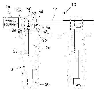
[0028] Figure 1 of the accompanying drawings illustrates a detonator system 10
according to the invention which includes a surface harness in the form of an
elongate two-wire bus 12 which extends to a plurality of boreholes 14 in rock
at a site
which is to be blasted. The bus 12 is connected to control equipment 16 which
is
used to control the blasting process. Each borehole contains a respective
detonator
20 which is connected via two wires 22 and 24, through the medium of an
appropriate connector 26, shown in dotted outline in each instance, to the two-
wire
bus 12.
CA 02777728 2012-04-13
WO 2011/140571 8 PCT/ZA2011/000025
[0029] Figure 2 illustrates in block diagram form certain components in a
detonator
20. The detonator has a processor or asic 30 and a circuit 32 which may be
distinct
from the processor/asic or which may be incorporated in the processor/asic.
The
circuit 32, in response to the detection by the processor/asic of at least one
designated or predetermined event 34, produces an output signal 36.
[0030] The connector 26 includes a sensing circuit 40 (shown in block form in
Figure
1) and at least one switch 42 which is operable by the sensing circuit under
certain
conditions as is described hereinafter. The operation of the connector is
described,
firstly, in general terms and then in more detail with specific reference to
Figure 4
which is a diagram of a circuit in the connector.
[0031] In the detonator system 10 the bus 12 has two wires 12A and 12B only
Each
detonator is connected by means of two wires 22, 24 only to the bus via a
corresponding connector 26. Once all the detonators have been connected to the
bus the control equipment 16 transmits a first command signal on the bus.
[0032] The first command signal is received by the first detonator i.e. the
detonator
which is closest to the control equipment. The remaining detonators, which are
downstream from the first detonator, are isolated from the first command
signal
because the switch 42, in the first connector, is open. An identity number can
be
assigned to, or can be read from, the first detonator and validation or other
checks
can be done on the first detonator. The first detonator can also be programmed
at
this stage, if required. The specifics of the detonator command sequences are
not
considered further herein as these are well known in the art and are
dependent, inter
alia, on the design of the detonator.
CA 02777728 2012-04-13
WO 2011/140571 9 PCT/ZA2011/000025
[0033] Commands to' the first detonator from the control equipment are
processed
by the processor 30 in the detonator. A signal 36, in response to the
commands, is
generated by the circuit 32 using techniques which are known in the art. The
signal
36, shown in a representative manner only in Figure 3, is at a first level of
current
modulation and comprises a plurality of pulses 36A (Figure 3). Each pulse has
a
relatively low level 46 of current amplitude and the sensing circuit 40 is not
responsive thereto. The pulses 36A thus pass through the connector 26, from
the
detonator to the control equipment 16, without any effect on the sensing
circuit 40. In
this manner secure and effective two-way communication between the control
equipment and the first detonator is established.
[0034] Assume that at least one designated event occurs. This event may be
selected for the purpose and, by way of example only, may be one or more of
the
following:
a) the end of a sequence of commands to the detonator from the control
equipment;
b) reception of a command, by the detonator, that is not addressed to the
detonator by the control equipment;
c) a state change in the detonator. The state change may be one or more of the
following:
i) the assignment of an identifier to the detonator;
ii) the reading of a detonator identifier;
iii) the programming of the detonator; and
iv) the assignment of a time delay to the detonator;
d) an instruction from the control equipment to the detonator to activate or
deactivate at least one switch in the connector;
CA 02777728 2012-04-13
WO 2011/140571 10 PCT/ZA2011/000025
e) the expiry of a time period during which no commands are received by the
detonator; and
f) a variation (decrease or increase) in the average voltage level on the two-
wire
bus.
[0035] For example validation checks may have been carried out successfully on
the
first detonator and an identifier may have been assigned to the first
detonator. When
this occurs the processor 30 (in the first detonator) actuates the circuit 32
to produce
a second output signal 36B (see Figure 3) which has a level 48 of current
modulation
which is significantly higher than the level 46 of current modulation for the
first signal
36A. The sensing circuit 40 in the connector is responsive to the higher level
of
current modulation and, upon detecting the signal 36B, the circuit 40 causes
closure
of the corresponding switch 42 (referring to Figure 1). The control equipment
can
then address the second detonator in the sequence in a unique and secure
manner.
Command signals directed to the second detonator are prevented from reaching
the
first detonator through the use of suitable links.
[0036] For example a command signal may be uniquely linked to the first or
second
detonator, or to the state of the first or second detonator, in a way which
ensures that
the signal can only reach the second detonator.
[0037] The aforementioned process continues in succession down the two-wire
bus.
Each detonator thus, in sequence, is uniquely and directly addressable by the
control
equipment 16 in a manner which allows for secure bidirectional communications.
Each detonator, in turn, is uniquely identified. Upon the occurrence of a
designated
or predetermined event at each detonator the following detonator is enabled in
the
sense that it is connected to the control equipment by closure of the switch
in the
preceding connector. An inherent time delay of a minimum duration is not
CA 02777728 2012-04-13
WO 2011/140571 11 PCT/ZA2011/000025
associated with each connector and switch closure takes place in the shortest
possible time.
[0038] The switch 42, in the illustrated example, is closed by the second
signal 36B
which is generated by the circuit 32 of the associated detonator upon
detection of a
predetermined event by the associated processor/asic 30. It is possible for
the circuit
32 to generate a third signal, not shown, at a level of modulation which is
distinct
from the levels 46 and 48. The sensor 40, or an additional sensor, could be
responsive to the third signal and this could be used to open the switch 42.
[0039] In a variation of the invention (shown in Figure 5) each connector
(marked
26A) includes two switches 42A and 42B respectively, each of which is
responsive to
a signal from the circuit 32 with a respective degree of modulation. The
switches
42A and 42B are in series and, in this event, at least two predetermined
events
would have to be detected for both switches to be closed and to be kept closed
so
that a succeeding detonator could be connected to the control equipment.
[0040] Figure 4 is a circuit diagram of a detonator 20 and a connector 26
which, as
noted, includes a sensing circuit 40 and at least the first switch 42.
[0041] The connector circuit includes four field effect transistors 50, 52, 54
and 56
respectively (which are used to implement the switching action of the switch
42,
notionally shown in Figure 1), input terminals 60 and 62, and output terminals
64 and
66 respectively. A resistor 68 is connected in line with the wire 22 to the
detonator
20.
[0042] A capacitor 70 is connected across the gate and source of each of the
transistors 50 and 52 respectively. A capacitor 72 is connected across the
gate and
source of each of the transistors 54 and 56 respectively.
CA 02777728 2012-04-13
WO 2011/140571 12 PCT/ZA2011/000025
[0043] Assume that the terminal 60 is positive with respect to the terminal
62. The
current to the detonator 20 passes through the resistor 68. In normal
operation, or
during talk back from the detonator to the control equipment 16, the voltage
developed across the resistor 68 is insufficient to switch either of the
transistors 50
and 52 on. Thus the transistors 54 and 56 are held off. As a result voltage
modulated signals, from the control equipment 16 to the detonator, that are
present
at the terminals 60 and 62 are not present at the terminals 64 and 66, i.e.
the switch
42 (shown in Figure 1) is effectively off.
[0044] If the detonator draws a higher current then the voltage across the
resistor 68
increases and the transistors 50 and 52 are turned on. When the transistor 52
turns
on the transistor 54 turns on and so does the transistor 56. The transistor
56, when
turning on, produces a latching action in that the transistor 50 is held on
even though
the voltage across the resistor 68 might drop below the initial high value at
which the
transistors 50 and 52 were turned on. The voltage across the resistor 68 would
drop
in this way when the high.current consumption or sink of the detonator 20
terminates.
[0045] At this stage each of the transistors 50 to 56 is conducting. This
remains the
case even for brief alternate polarity signalling on the terminals 60 and 62
for the
capacitors 70 and 72 respective hold the transistors 50 and 54 on.
[0046] Consequently a signal which is presented at the terminals 60 and 62 is
present at the terminals 64 and 66. If power is removed from the terminals 60
and
62, or if the polarity of the signal applied to these terminals is reversed
for a
sufficiently long period to allow either of the capacitors 70 and 72 to
discharge, the
switch (42) embodied in the connector opens. Diodes 80 and 82 prevent the
capacitors 70 and 72 from discharging forcibly if the polarity at the
terminals 60 and
62 is reversed by the control equipment. These capacitors normally discharge
via
CA 02777728 2012-04-13
WO 2011/140571 13 PCT/ZA2011/000025
resistors 84 and 86 which are connected in parallel with the capacitors, with
a
polarity reversal or if power is removed.
[0047] In the circuit shown in Figure 4 switching is effected in both wires
12A and
12B of the two-wire bus. The circuit of the connector can however be
reconfigured to
use fewer components or to effect switching in only one of the wires 12A and
12B.
[0048] The principles described herein can be used, with substantial benefit,
in
conjunction with known techniques in the art and, in particular, in
combination with
the markers which are described in the specification of International Patent
Application No. PCT/ZA2004/00079 to provide flexible or various time delays to
the
detonators or to adjust these time delays. Clearly time assignments or delays
can be
transmitted from the control equipment 16 to respective detonators.
[0049] In Figure 1 the two-wire bus 12 is shown as a separate component. This
however is not necessarily the case for the bus could be formed as part of the
harnesses or wires 22 and 24 which extend to the respective detonators.
[0050] The functioning of the connector 26 is preferably carried out by means
of
circuitry included in a housing of the connector. An equivalent effect, which
is
intended to fall within the scope of the present invention, can however be
achieved
by providing suitable circuitry in an appropriate module which is associated
with the
detonator wires 22, 24, if required.
[0051] In the arrangement shown in Figure 1 it is assumed that the two-wire
bus 12
is laid out and that, when a connector is coupled to the bus, a break in one
of the
wires (in the illustrated example the wire 12B) is made. This is in accordance
with
the techniques described in the specification of South African Patent
Application No.
2009/06238. This is not necessarily the case for in an alternative arrangement
CA 02777728 2012-04-13
WO 2011/140571 14 PCT/ZA2011/000025
suitable lengths of the two-wire bus are connected individually between
respective
adjacent pairs of connectors.
[0052] The circuit shown in Figure 4 is polarity-sensitive in that the
terminal 60 must
be positive with respect to the terminal 62 during switching. It is possible
though, to
reconfigure the circuit so that it can function in a polarity-insensitive
manner.