Note: Descriptions are shown in the official language in which they were submitted.
81593852
HIGH SPEED LASING DEVICE
The present invention relates to lasing devices for use in high-speed fiber
optical communication
systems, and more specifically to Vertical Cavity Surface Emitting Lasers
(VCSELs) with high
modulation bandwidth. Moreover the present invention relates to optical
interconnects including
lasing devices with high modulation bandwidth. Finally, the present invention
relates to a method
for manufacturing high-speed lasing devices.
Lasing devices and in particular Vertical Cavity Surface Emitting Lasers
commonly used in high-
speed communication systems include a cavity sandwiched between two highly
reflective
mirrors or reflectors so as to form a resonator. The mirrors include several
alternating layers of
semiconductors of high and low refractive index and are doped with p-type and
n-type dopants
or {impurities, respectively so as to form a p-n or a p-i-n diode junction. In
a semiconductor laser
the gain mechanism that generates the lasing is provided by light generation
from the
recombination of holes and electrons. The recombining holes and electrons are
injected,
respectively, from the p and n sides of the diode junction. In
telecommunication applications, the
recombination of carriers is generated by electrical pumping, i.e. by forward-
biasing the diode
junction. Commonly, the current in the lasing device is confined to an
aperture of the laser by
implanting ions into the lasing device structure everywhere except the
aperture on the lasing
device so as to increase the electrical resistivity of the material around the
aperture.
Alternatively, the current around the aperture of the lasing device can be
inhibited by oxidizing
the material around the aperture of the lasing device.
Semiconductor lasers are employed in telecommunication applications for
building optical
interconnects used in electronic devices. Such optical interconnects became in
recent years
widely used in electronic devices due their capability of supporting a much
higher bandwidth
than traditional cable interconnects. In this context, the development of
optical modules for
converting optical signals into electrical signals and vice versa plays a
crucial role in a wide
range of applications, such as mid-board applications using optical
interconnects.
Semiconductor lasers, such as VCSEL, typically convey information according to
two schemes.
In the first scheme, the laser is maintained in a constant light-emitting
state and the output
intensity is modulated by means of an external modulator driven by an
externally applied
voltage. Since this first scheme requires a costly external apparatus, optical
interconnects
including VCSEL are generally directly modulated. Direct modulation involves
changing the
current input of the laser, or, in other words, modulating the current around
the bias current so
CA 2778625 2018-02-26
81593852
2
as to produce a time-dependent output in the optical intensity. Usually, the
current is switched
between two values, both larger than the threshold current of the device.
Figure 7 shows a lasing device 4000 according to the state of the art. The
lasing device includes
a substrate 4030 made of semiconductor material, a first mirror 4300 and a
second mirror 4100.
The first and second mirrors 4300 and 4100 respectively include a stack of
alternating
semiconductor mirror layers 4310, 4320. The layers 4310 have a high refractive
index while the
layers 4320 have a low refractive index. The first mirror 4300 is doped with n-
type dopants, while
the second mirror 4100 is doped with p-type dopants. The lasing device 4000
further includes a
cavity spacer 4200 between the first and second mirrors 4300, 4100. The cavity
spacer 4200
includes a first cladding layer 4230 and second cladding layer 4210 and an
active layer 4220.
Finally, the lasing device 4000 includes a current-confining region 4020 which
defines a current-
confining aperture 4021. The current-confining region is formed in the second
cladding layer
4210 immediately below the second mirror 4100.
Figure 8 is a schematic drawing illustrating the working principle of the
lasing device 4000 of
figure 7. In particular, figure 8 shows the effect of direct modulation on the
carrier density in the
active layer of the lasing device 4000. The current is switched between two
values, both larger
than the threshold current of the device. In the lasing device 4000, the
carrier density is not
perfectly clamped, but swings with the injection current due to gain
saturation with optical field
intensity and gain reduction due to internal heating.
Figure 8 shows the distribution of the intensity of the optical field along
the active layer 4220. As
can be seen from the dashed line plot, the intensity of the optical field is
maximum in the zone of
the active layer corresponding to the current-confining aperture 4021. The
optical field intensity
is generally lower atthe periphery and higher in the center of the active
region. Moreover, in the
peripheral regions of the active layer, optical loss is also higher than in
the center of the active
layer. This leads to a lower stimulated recombination rate at the periphery of
the active layer.
Upon switching from the high current level to the lower current level, the
carrier density in the
active layer 4220 will also switch from a high to a lower level. As can be
seen from figure 8, at a
particular bias current above the threshold, the carder density distribution
in the active layer
4220 is illustrated by the dotted curve (3). Zone A of the active layer 4220
indicates the area
where the optical gain reaches the threshold value. Outside zone A, the
carrier density is not
sufficient for the generated gain to reach the threshold value. In addition,
within zone A, the
carrier density is not constant, but is larger where the local temperature
and/or local photon
density are higher.
CA 2778625 2018-02-26
81593852
3
Figure 8 illustrates the particular case, in which the carrier density
increases towards the center
of the aperture.
At a .higher bias current, both the temperature and the photon density in the
active layer 4220
increase. Consequently, the carrier density in zone A will also increase in
order to maintain the
gain at the threshold value. At a higher bias current, the carrier density in
the areas surrounding
zone A will also increase and will become high enough to generate a gain that
reaches the
threshold value in a zone B surrounding zone A. This behaviour is illustrated
by the dashed
curve (1). Consequently, the active region of the laser where the carriers and
photons are
strongly coupled through stimulated recombination will expand from zone A at a
lower bias to
zones A and B at a higher bias current.
Upon switching from a high bias to a low bias, the carrier density in zone A
of the active layer
decreases at a much faster rate than the density in zone B of the active layer
4220 due to a
stronger stimulated recombination in the areas with a higher optical field
intensity. Thus, the
carrier density will have two peaks at the periphery of the active layer 4220
as shown in the solid
curve (2). These excess carriers in zone B of the active layer 4220 will act
as a reservoir from
which carriers will flow from the periphery towards the center of the active
layer 4220, thereby
acting as a capacitance connected parallel to the active layer of the laser.
This extends the fall-
time of the lasing device 4000 and negatively affects its response to a
modulating signal.
Consequently, the design of common lasing devices limits the modulation
bandwidth and the
high speed performance of optical interconnects employing the lasing device.
More precisely, since during the high-to-low transition, the laser 4000
evolves towards a lower
carrier density and a reduced stimulated recombination rate the laser 4000
slows down in
adapting to the new, lower current level, thereby enhancing the effect of the
excess carrier
density at the periphery of the active layer on extending the fall time. Even
if the optical field
intensity returns to its nominal value after a current waveform is applied,
the carrier density will
not, thereby leading to a dynamical coupling from the past to the future
causing, for instance,
inter-symbol interference.
In addition, in devices wherein current confinement is obtained by using a
layer of insulation
oxide 4020, the effective parasitic capacitance associated with the isolation
oxide defining the
current confining aperture is determined by the capacitance across the
oxidized layer 4020 in
series with the capacitance of the diode junction underneath the oxidized
layer. If the diode is
unbiased, the effective capacitance is given by the oxide layer capacitance in
series with the
depletion capacitance of the diode, the latest being the lowest of the two.
Under forward bias the
CA 2778625 2018-02-26
81593852
4
capacitance of the diode will increase while its series resistance will
decrease leading to an
overall increase of the effective capacitance of the structure. The maximum
capacitance is only
limited by the oxide capacitance, which is relatively large.
Lateral carrier spreading out from the aperture formed in the oxidized layer
4020 can be
significant and in a steady-state, this will lead to a leakage current. The
lateral carrier spreading
will also provide some degree of forward bias to the outer regions of the
diode structure under
the isolation oxide 4020, thereby leading to an increase of the effective
parasitic capacitance of
the device with bias.
The above described effect further limits the modulation speed of the lasing
device and hence
the modulation bandwidth.
In order to overcome the problems associated with direct modulation of common
lasing devices,
many solutions have been proposed for reducing the effect of carrier spreading
out towards the
periphery of the active layer. In particular, clamping of the carrier density
inside the active region
could be improved through reduced gain saturation and internal heating.
Alternatively, proton
implantation or patterned tunnel junction techniques may be used to
additionally confine the
carriers so as to reduce the carrier density at the periphery of the active
layer.
The known techniques have, however, the disadvantage that the additional
confinement is
effective only if the lateral geometry of the carrier confinement features
matches the transversal
distribution of the optical field. Developing a device with the above
mentioned design requires
extensive design and is very complex and costly to realize.
Therefore, the problem underlying the present invention is to provide a lasing
device for use in
directly modulated high-speed fiber optical communication systems, which can
be driven at a
high-modulation speed, which has a reduced effective parasitic capacitance,
and which can be
fabricated in a particularly simple and cost-effective manner and at the same
time allows for a
faster and more reliable fiber optical communication system.
This problem is solved by providing a laser structure including, at the
periphery of the active
layer of the main laser, an auxiliary laser having the function of a guard
laser. The guard laser
will clamp the carrier density within its active region which overlaps the
periphery of the active
region of the main laser and further induce additional stimulated
recombination at the periphery
of the active region of the main laser.
CA 2778625 2018-02-26
81593852
The additional stimulated recombination will increase the rate at which the
excess carrier density
at the periphery of the active region decreases when the input current is
switched down. In
addition, the guard laser causes a reduction of the carrier injection in the
outer region of the
diode structure, thereby limiting the increase of the effective parasitic
capacitance related to an
oxide layer. Finally, the solution proposed in the present invention does not
require using
elaborated and costly techniques such as ion implantation or patterned tunnel
junction.
According to a preferred embodiment the present invention provides a lasing
device for use in
an optical interconnect. The lasing device comprises a first reflector and a
second reflector; a
confinement layer adapted to confine current within a current-confining
aperture, and an active
layer between the first and second reflectors. The active layer comprises a
main active region
aligned with the current confining aperture and an auxiliary active region
surrounding the main
active region. The second reflector includes a first reflector region arranged
on the current-
confining aperture and a second reflector region surrounding the first
reflector region. The
second reflector region and the first reflector are configured to induce
stimulated recombination
in the auxiliary active region.
In this manner, although the periphery of the active layer is electrically
isolated through the
confinement layer and the carrier density is not clamped throughout the active
layer, the excess
of carriers that accumulates at the periphery of the main active region can be
consumed by
means of stimulated recombination induced by the second reflector region.
Since the excess
carriers at the periphery of the main active region are consumed by the
additional stimulated
recombination, the capacitive effect due to the flow of carriers from the
periphery to the center of
the main active region is suppressed.
According to a further advantageous development, the reflectance of second
reflector region
may be higher than the reflectance of the first reflector region. The higher
reflectance of the
second reflector region increases the intensity of the optical field at the
periphery of the main
active region and consequently the recombination rate of the carriers.
Moreover, the higher
reflectance of the second reflector region decreases the lasing threshold in
the auxiliary active
region. The higher recombination rate consumes the excess of carriers, thereby
preventing the
formation of a reservoir of carriers at the periphery of the main active
region.
According to another development, the first reflector region is aligned with
the current confining
aperture and the area of the first reflector region is larger than the area of
the current confining
aperture. In particular, if the current confining aperture has a circular
shape, also the first
reflector region is chosen to be circular and the diameter Di of the first
reflector region is larger
CA 2778625 2018-02-26
81593852
6
than the diameter Do of the current confining aperture. In this case, the
second reflector region is
chosen to be ring-shaped with an inner diameter D2 that may be equal to or
larger than the
diameter Di of the first reflector region.
In a further development a ratio Si/So between the area of the first reflector
region and the
area of the current confining aperture may be in the range from 1.0 to 3.3.
The relation
between the sizes of the current confining aperture and the first reflector
region allows to control
the coupling between the main laser and the guard laser, and consequently the
effectiveness of
the guard laser on reducing the capacitive effect of the excess carriers at
the periphery of the
main laser.
In a lasing device according to an advantageous realization of the invention,
the first reflector
and the second reflector respectively include at least one layer with high
refractive index and
one layer with low refractive index. The layers can be easily grown by
standard techniques and
the so obtained reflector has an optimal reflectance of above 99.5%.
A layer of the second reflector may be fabricated so as to be thicker in the
second reflector
region than in the first mirror region. The thickness of a topmost reflector
layer of the second
reflector may be chosen to be an odd-number of a quarter wavelength in the
second reflector
region and zero or an even number of a quarter wavelength in the first
reflector region. In this
manner the first reflector region and the second reflector region can be
easily defined by simply
performing a further step in the manufacturing process of a conventional
lasing device.
In an alternative advantageous realization of the present invention, the
second reflector may
include a reflector element arranged on the second reflector region and
adapted to increase the
reflectance of the second reflector region. Accordingly, the reflectivity of
the second reflector can
be selectively adjusted so as to form the first and second reflector regions
by growing or
mounting an additional layer on top of the second reflector, without involving
any etching and
masking process.
In an embodiment of the present invention, the first reflector region, the
main active region and
the first reflector define a main laser, and the second reflector region, the
auxiliary active region
and the first reflector define an auxiliary laser.
The lasing device of the present invention may further include a first
cladding layer and a second
cladding layer. The first and second cladding layers sandwich the active layer
there-between so
as to form a cavity spacer. The length of the cavity spacer may be chosen so
as to correspond to
CA 2778625 2018-02-26
= 81593852
7
an integer number of half waves at the emission wavelength. The thickness of
the
cavity spacer defines the resonance and the emission wavelength.
According to a further development of the present invention the active layer
includes
a stack of a plurality of alternating quantum wells and barriers and a
vertical
confinement layer on either side thereof.
The lateral confinement layer may be arranged between the first reflector and
the
second reflector and may include an oxidized layer of semiconductor or an ion
implanted region surrounding the current-confinement aperture.
According to a further advantageous development of the present invention, the
first
reflector region is disk-shaped and the second reflector region is ring-
shaped.
An embodiment of the present invention relates to an optical module including
the
lasing device described above. The above described lasing devices have a
reduced
carrier density at the periphery of the active region and do not suffer of
carries flowing
back from the periphery towards the center of the main active region upon
switching
from high to low driving currents. Consequently, the optical module can be
driven at
high modulation speeds. Optical interconnects mounting said lasing devices can
therefore be used in high-speed fiber optical communication systems having an
increased modulation bandwidth.
A further embodiment of the present invention provides a method for forming a
lasing
device for use in an optical interconnect. The method includes forming a first
reflector
stack on a semiconductor substrate and a confinement layer. The confinement
layer
is adapted to confine current within a current-confining aperture. An active
layer is
formed on the first reflector stack, and comprises a main active region
aligned with
the current confining aperture and an auxiliary active region surrounding the
main
active region. A second reflector stack is formed on the active layer, and in
the
second reflector stack a first reflector region is arranged on the current-
confining
aperture. A second reflector region surrounding the first reflector region is
further
CA 2778625 2018-02-26
81593852
7a
formed, wherein the second reflector region and the first reflector are
configured to
induce stimulated recombination in the auxiliary active region.
According to one aspect of the present invention, there is provided a lasing
device for
use in an optical interconnect, the lasing device comprising: a first
reflector and a
second reflector; a confinement layer, said confinement layer being adapted to
confine current within a current-confining aperture; an active layer between
the first
and second reflectors, said active layer comprising a main active region
aligned with
the current confining aperture and an auxiliary active region surrounding the
main
active region and overlapping the periphery of the main active region, the
auxiliary
active region being a zone of the active layer including carriers that leaked
from the
main active region; wherein the confinement layer is between the active layer
and the
second reflector and wherein the second reflector includes a first reflector
region
arranged on the current-confining aperture and a second reflector region
surrounding
the first reflector region, the first reflector region, the main active region
and the first
reflector defining a main laser; wherein the second reflector region, the
auxiliary
active region and the first reflector define an auxiliary laser; and wherein
the second
reflector region and the first reflector, are configured to induce stimulated
recombination in the auxiliary active region so that a carrier density is
clamped within
the auxiliary active region and additional stimulated recombination is induced
at the
periphery of the main active region, wherein a reflectance of second reflector
region
is higher than a reflectance of the first reflector region.
According to another aspect of the present invention, there is provided a
method for
forming a lasing device for use in an optical interconnect, the method
including:
forming a first reflector on a semiconductor substrate; forming a confinement
layer,
said confinement layer being adapted to confine current within a current-
confining
aperture, forming an active layer aligned with the current confining aperture
and an
auxiliary active region surrounding the main active region; forming a second
reflector
above the active layer and above the confinement layer; the second reflector
includes
a first reflector region arranged on the current-confining aperture and a
second
CA 2778625 2018-02-26
81593852
7b
reflector region surrounding the first reflector region, wherein a reflectance
of second
reflector region is higher than a reflectance of the first reflector region;
defining a
main laser from the first reflector region, the main active region and the
first reflector;
defining an auxiliary laser from the second reflector region, the auxiliary
active region
and the first reflector; and wherein the second reflector region and the first
reflector,
are configured to induce stimulated recombination in the auxiliary active
region so
that a carrier density is clamped within the auxiliary active region and
additional
stimulated recombination is induced at the periphery of the main active
region.
The accompanying drawings are incorporated into and form a part of the
specification
to illustrate several embodiments of the present invention. These drawings
together
with the description serve to explain the principles of the invention. The
drawings are
only for the purpose of illustrating preferred and alternative examples on how
the
invention can be made and used
CA 2778625 2018-02-26
81593852
8
and are not to he construed as limiting the invention to only the illustrated
and described
embodiments. Further, features and advantages will become apparent from the
following and
more particular description of the various embodiments of the invention as
illustrated in the
accompanying drawings, in which like reference numbers refer to like elements
and wherein:
Figure 1 shows a sectional view of a lasing device according to a first
embodiment of the
present invention;
Figure 2 shows a sectional view of a lasing device according to a
further embodiment of
the present invention;
Figure 3 shows a sectional view of a lasing device according to a
further embodiment of
the present invention;
Figure 4 shows a particular of the laser cavity used in the lasing
device of figures 1 to 3
according to a preferred embodiment of the present invention;
Figure 5 schematically shows the working principle of a lasing device
according to a
=
preferred embodiment of the present invention;
Figure 6 shows a sectional view of an optical interconnect mounting a
lasing device
according to the present invention;
Figure 7 shows a sectional view of a conventional lasing device
according to the prior art;
Figure 8 shows the working principle of a common lasing device according
to the prior art.
In the following description, for explanatory purposes, specific details are
set forth in order to
provide a thorough understanding thereof. However, it may be evident that the
present invention
can be practiced without these specific details. Furthermore, well known
structures and devices
are only described in a more general form in order to facilitate the
description thereof.
In the following description the expressions "mirror" and "reflector" are used
to indicate the
stacks of semiconductor or dielectric layers defining the resonant cavity of
the laser. Similarly the
expressions "first mirror region" and "first reflector region" are used in the
following with the
same meaning; and the expressions "second mirror region" and "second reflector
region" are
used in the following with the same meaning. The expression "gain region" and
"cavity spacer"
indicate the semiconductor layers sandwiched between the reflectors of the
lasing device.
CA 2778625 2018-02-26
81593852
9
The problem underlying the present invention is based on the observation that
upon switching
down the driving current in direct-modulated lasing devices, the carrier
density will decrease at a
much faster rate at the center than at the periphery of the active layer. This
is due to the fact that
in the areas with higher optical field intensity, i.e. the center of the
active layer, stimulated
recombination is stronger. Accordingly, an excess of carriers accumulates in
the periphery of the
active layer, which acts as a carrier reservoir, and a lateral redistribution
of carriers from the
periphery towards the center of the active layer can take place. During a high-
to-low transition,
the laser evolves toward a lower photon density and a reduced recombination
rate. This will
enhance the effect of the excess carrier density at the periphery of the
active layer, thereby
extending the fall time of the lasing device. Moreover, lasing devices using
an oxide
semiconductor layer for confining the current in the device may suffer from
lateral carrier
spreading, resulting in a leakage current and an increase of the effective
parasitic capacitance of
the device with bias.
According to the present invention, the modulation of the carrier distribution
at the periphery of
the active layer is reduced by implementing an auxiliary laser, or guard
laser, at the periphery of
the main laser. The guard laser will clamp the carrier density within its
active layer and consume
the excess carriers at the periphery of the active layer of the main laser
through stimulated
recombination. In addition, the guard laser will reduce the carrier injection
in the outer regions of
the diode structure forming the lasing device, thereby limiting the increase
of the effective
parasitic capacitance related to the oxide layer.
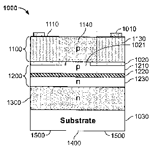
Figure 1 illustrates a sectional view of a lasing device designed according to
the principles of the
present invention. The lasing device 1000 comprises a substrate 1030 of
semiconductor material
on top of which a first reflector or mirror 1300 is formed. The first
reflector 1300 may be any
semiconductor material with a high reflectivity. A cavity spacer 1200 is
further provided on top of
the first mirror 1300. The cavity spacer 1200 includes a first cladding layer
1230 and a second
cladding layer 1210 which are doped with opposite conductivity types. An
active layer 1220 is
sandwiched between the first and second cladding layers 1230 and 1210. The
active layer 1220
is made of an intrinsic semiconductor and is the layer in which recombination
of carriers occurs
when the laser is driven by electrical or optical pumping. A closer
description of the gain region
1200 is given with reference to figure 4.
The lasing device 1000 further includes a confinement layer 1020, which
defines a current
confining aperture 1021. The confinement layer 1020 is a layer of oxidized
semiconductor
material or oxidation layer. The oxidation layer 1020 is generally obtained by
growing a high
CA 2778625 2018-02-26
81593852
content aluminum semiconductor layer within the lasing device 1000 and further
oxidizing the
layer. The oxidized portion is electrically non-conductive and also has
a"lower refractive index,
which also provides some degree of confinement for the optical field generated
in the active
layer 1220. The current confining aperture 1021 is a non-oxidized portion of
the oxidation layer
1020. The current and the optical field generated by forward biasing the
lasing device 1000 are
mostly confined within the current-confinement aperture 1021.
A second reflector 1100 is formed on top of the current confinement layer
1020. The first and
second mirrors or reflectors 1300 and 1100 are doped with impurities so as to
have opposite
conductivity types and form a diode junction. The second mirror 1100 and the
second cladding
layer 1210 are p-type, while the first mirror 1300 as well as the first
cladding layer 1230 are n-
type. The active layer 1220 includes one or more layers of an intrinsic
semiconductor.
According to the structure in figure 1, the lasing device 1000 is a p4-n diode
junction. However,
other configurations different from the described one may be used according to
the particular
application of the lasing device 1000. Further, in an alternative realization,
the first and second
mirrors 1300, 1100 may be intrinsic semiconductors or dielectric and p-type
and n-type
semiconductor layers may be buried between the first and second mirror 1300,
1200, to provide
electrical connection to the active layer 1220.
The second mirror 1100 includes a first mirror region 1140 and a second mirror
region 1130
surrounding the first mirror region 1140. The reflectance of the second mirror
region 1130 R2 is
selected to be higher than the reflectance R1 of the first mirror region 1140.
The first mirror
region 1140 is formed in the second reflector 1100 above the current-confining
aperture 1021.
The area of the first mirror region 1140 is larger than the area of the
current confining aperture
1021 and also partially overlaps a portion of the oxidation layer 1020
immediately surrounding
the current confining aperture 1021. However, in other preferred realizations
of the present
invention the first mirror region 1140 may be chosen to have the same size as
the current-
confining aperture 1021, or a smaller size.
The first and second reflector regions 1140, 1130 may be obtained by adding a
top reflector
1110 on the top surface of the second mirror 1100. The top reflector 1110 may
be a distributed
Bragg reflector made of dielectric layers of alternate high and low refractive
indices, a metal
reflector, or a combination thereof.
Upon forward biasing the lasing device 1000 holes and electrons will
respectively move from the
p-doped layer 1210 and the n-doped layer 1230 to the active layer 1220.
Recombination of holes
CA 2778625 2018-02-26
81593852
11
and electrons injected into the active layer 1200 from the p and n sides of
the p-i-n junction
produces emission of light. The first and second mirrors 1300 and 1100 between
which the
active layer 1220 is sandwiched form together with the cavity spacer 1200, a
resonant cavity in
which the light is reflected before being emitted from the lasing device 1000.
The first mirror region 1140, the portion of the cavity spacer 1200
corresponding to the area of
the first mirror region 1140 and arranged there-below, and the first
dielectric mirror 1300 define a
main laser 1400, which emits light with wavelengths depending on the energy
gap of the
semiconductor materials used for fabricating the lasing device 1000 and on the
thickness of the
cavity spacer. Similarly, the second mirror region 1130 surrounding the first
mirror region 1140,
the portion of the cavity spacer 1200 below it and the first dielectric mirror
1300 define an
auxiliary laser 1500, or guard laser. The guard laser 1500 surrounds the
portion of the lasing
device 1000 defining the main laser 1400. The portion of the active layer 1220
surrounding the
current confining aperture 1021 and arranged below the second mirror region
1130 is isolated
through the oxidation layer 1020. Therefore, holes can not be injected
directly from the p-type
mirror into said portion of the active layer. Instead, carriers leak from the
center of the active
region 1220, which corresponds to an active region of the main laser 1400 into
the periphery of
the active region 1220, which corresponds to the active region of the
auxiliary laser 1500. In
other words, the recombining carriers of the auxiliary laser 1500 are injected
from the center of
the active layer 1220. Details of the active layers and on the different
regions of the active layer
will be given with reference to figure 5.
The carrier density in the center of the active layer 1220 corresponding to
the first mirror region
1140 at and above the threshold current generally depends on the threshold
gain in the active
layer and thus on the reflectance of the dielectric mirrors 1100 and 1300.
Generally, the carrier
density at the threshold is inversely proportional to the reflectance of the
electric mirror 1100 and
1300 of the lasing device. In the lasing device of the invention, the
reflectance R2 of the second
mirror region 1130 is higher than the reflectance of Ri of the first mirror
region 1140. This
configuration provides for a lower threshold carrier density of the auxiliary
laser 1500. A more
detailed description of the design of the main and auxiliary lasers 1400, 1500
and the
corresponding active layers will be given with reference to figure 5.
In vertical cavity surface emitting lasers the reflectivity of the mirror 1300
is in the range of about
99.5 to 99.9%. This value can be lower in case of edge emitting lasers.
The details regarding the working principle of the lasing device 1000 also
apply to all the other
embodiments of the present invention as described in figures 2 to 5.
CA 2778625 2018-02-26
81593852
12
The lasing device 1000 of figure 1 further includes first terminal contacts 10
arranged on the top
surface of the second mirror 1100 and second terminal contacts arranged on the
bottom surface
of the substrate (not shown).
Figure 2 shows a further embodiment of a lasing device 2000 according to the
present invention.
The lasing device 2000 includes a substrate 2030, a first mirror 2300, a
cavity spacer 2200
including a first cladding layer 2230 and second cladding layer 2210 doped
with opposite
conductivity types, a second mirror 2100 and a current confinement layer 2020
sandwiched
between the second cladding layer 2210 and the second mirror 2100. The first
mirror 2300 and
the second mirror 2100 are doped so as to achieve opposite conductivity types.
In particular, the
first reflector 2300 and the first cladding layer 2230 are doped with n-type
dopants and the
second reflector 2100 and the second cladding layer 2210 are doped with p-type
dopants. The
current-confining layer 2020 includes a current-confining aperture 2021.
The second mirror 2100 includes a first mirror region 2140 corresponding to
the current
confinement aperture 2021. The area of the first mirror region 2140 is larger
than the area of the
current-confining aperture 2021 and may partially extend over the portion of
the current
confinement region 2020 immediately surrounding the current confining aperture
2021.
In an advantageous example, the ratio between the area S1 of the first mirror
region 2140 and
the area So of the current confinement aperture 2021 may be about 1.4. The
above value is not
universal and may change depending on the particular design of the lasing
device. More
precisely, the optimum ratio Si/So may be chosen based on the details of the
particular
realization, for instance, on the number of quantum wells and the composition
of the quantum
wells and barrier layer, and the actual reflectance of the first and second
reflectors. The optimum
ratio may be conveniently found by direct experimentation. As an example,
several devices with
first mirror regions having different areas SI may be processed on one
substrate, such as a
semiconductor wafer. The optimum design may be found by direct measurement of
parameters
such as the threshold current, differential efficiency and modulation
bandwidth, and/or the rise
and fall times of the optical signal generated when a modulated current is
applied to the device.
For many practical configurations commonly used in telecommunication
applications the ratio
Si/So may be advantageous chosen in the range of 1.0 to 3.3.
In one particular configuration, the current confining aperture 2021 as well
as the first mirror
region 2140 may have a circular shape. In this case the diameters Do and Di of
the current
confining aperture and the first mirror region may be used as parameters.
Accordingly, the ratio
between the outer diameter D1 of the first mirror region 2140 and the diameter
Do of the current-
CA 2778625 2018-02-26
81593852
13
confining aperture 2021 may be 1.2. Also in this case, the optimum ratio Dl/D2
depends on the
details of the particular realization, for instance, on the number of quantum
wells and the
composition of the quantum wells and barrier layer, and the actual reflectance
of the first and
second reflectors. The optimum ratio may be conveniently found by direct
experimentation. As
an example, devices with several different DI values may be processed on one
substrate. The
optimum design may be found by direct measurement of parameters such as the
threshold
current, differential efficiency and modulation bandwidth, and/or the rise and
fall times of the
optical signal generated when a modulated current is applied to the device.
For many practical
configurations it may be advantageous to explore a range of 1.0 to 1.8 for the
ratio Di/Do.
The current confinement region 2020 may be an oxidation layer as described
with reference to
figure 1 or may be obtained by ion, for instance proton, implantation in the
cladding layer 2210.
As an example, if the current confinement region is obtained by implantation,
ions such as
hydrogen ions and the like, may be implanted in the structure of the lasing
device, for instance in
the cladding layer 2210, everywhere except the current-confining aperture
2021. Ion
implantation destroys the lattice structure around the aperture, thereby
inhibiting the current flow
through this region.
In another alternative embodiment, current confinement may be obtained by a
patterned tunnel
junction. Finally, first terminal contacts 2010 are arranged on the top
surface of the mirror 2100
and second terminal contacts (not shown) are arranged on the bottom surface of
the substrate
2030.
The working principle of the lasing device 2000 is the same as the working
principle of the lasing
device 1000 and will not be explained again.
The first and second mirrors 2300 and 2100 are distributed Bragg reflectors
(DBR) structures.
The first mirror 2300 includes a stack of a first layer 2320 and a second
layer 2310 with
alternating high and low refractive indices. Each of the first and second
layers 2320 and 2310
has a thickness of a quarter of the laser wavelength in the material. The
layer composition of the
first mirror 2300 according to the above design yield an intensity
reflectivity in the range of 99%
to 99.9%. Similarly, the second mirror 2100 also includes a stack of a first
layer 2320 and a
second layer 2310 of alternating high and low refractive indices. In a
preferred realization of the
present invention, the first and second mirrors 2300, 2100 include 30 and 21
pairs of layers
2310, 2320, respectively. However, this configuration is not limiting and the
first and second
mirrors 2300, 2100 may include any number of layers, such as 22 layers for the
second DBR
2100 and 34 layers for the first DBR 2300.
CA 2778625 2018-02-26
81593852
14
Although in the particular embodiment of figure 2, the mirrors are made of
distributed Bragg
reflectors, the first and second mirrors of the lasing device 2000 may also be
obtained by other
means, such as using a thin metal-film arranged in a doped semiconductor layer
and the like.
The second reflector 2100 includes a first mirror region 2140 and a second
mirror region 2130.
The second mirror region 2130 has a higher reflectance than the first mirror
region 2140. This
can be obtained by adding a top reflector 2110 on the top surface of the
second mirror 2100.
The reflector 2110 may be an additional distributed Bragg reflector made of
semiconductor or
dielectric layers of alternate high and low refractive indices, a metal
reflector, or a combination
thereof.
Alternatively, the second mirror region 2130 can be obtained by modifying one
or more of the
second layers 2310 forming the second mirror 2100 by growing only part of the
structure,
patterning said structure and growing more layers or adding dielectric layers.
Still, in another embodiment, the second mirror region 2130 may be obtained by
modifying one
or more of the second dielectric layers 2310 forming the second mirror 2100 by
converting the
semiconductor layer in a similar way to the oxide aperture.
The shape of the additional reflector 2110 depends on the shape of the first
mirror region 2140
and on the design of the current-confining aperture 2021. More precisely, the
additional reflector
2110 is designed so as to surround the first mirror region 2140. In the
embodiment of figure 2,
the current-confining aperture 2021 has a circular shape, in which case the
second mirror 2130
and the additional reflector 2110 have a ring-shaped section. However, the
proposed solution
and the discussion thereof also apply to devices having current confining
apertures, first mirror
regions and second mirror regions of any shape.
The first mirror region 2140, the portion of the gain region or cavity spacer
2200 corresponding
to the area of the first mirror region 2140 and arranged below it, and the
first mirror 2300 define
a main laser 2400, which emits light having one or several wavelengths
depending on the
energy gap of the semiconductor materials used for fabricating the lasing
device 2000 and on
the thickness of the cavity spacer 2200. Similarly, the second mirror region
2130 surrounding the
first mirror region 2140, the portion of the cavity spacer 2200 below it and
the first mirror 2300
define an auxiliary laser 2500 or guard laser. The guard laser 2500 surrounds
the portion of the
lasing device 2000 defining the main laser 2400.
CA 2778625 2018-02-26
81593852
16
However, these devices may also be designed to emit light at other
wavelengths, such as 980
nanometers or 1,060 nanometers.
The lasing devices of figures 2 and 3 may be vertical Cavity Surface Emitting
Lasers (VCSELs).
The design of these VCSELs is based on a stack made of Gao.x)Alx-As layers.
The first and
second mirrors 2300, 2100 and 3100, 3300 are distributed Bragg reflectors
(DBRs), which use
layer pairs with alternating composition to provide the desired reflectance.
The cavity spacer
2200, 3200 is also Ga11.,0A1As where x is varied in order to provide desired
electrical transport
and confinement characteristics. The active layer 2220, 3220 includes a number
of GaAs
quantum wells (not shown) with Gao.x)AlõAs barriers (not shown). A more
detailed description of
the cavity spacer 2200, 3200 will be given with reference to figure 4. In an
alternative
embodiment, the active layer 2220, 3220 may include strained Gaci,olnõAs
quantum wells with
Ga11.,0AlxAs barriers. This solution is particularly advantageous in high
performance VCSELs,
since the Gao_x)InAs semiconductor material ensures a better performance and a
higher
reliability.
As a concrete example, the second DBR 2100, 3100 may be p-doped and the first
DBR 2300,
3300 may be n-doped. The substrate 2030, 3030 may be n-doped GaAs. The cavity
spacer
2200, 3200 is designed as a separate confinement structure and may be a layer
of Gao.x)AI,As
with graded x. As an example x may be in the range from 0.3 to 0.9. The active
layer 2220, 3220
may consist of 3 Ga(i..,01nxAs quantum wells, wherein x may be in the range
from 5 to 10%, with
Ga(r.õ)A1xAs barriers, wherein x is in the range from about 30 to about 40%.
On the p-side of the
lasing device 2000, 3000 between the second DBR mirror 2100, 3100 and the
cavity spacer
2200, 3200 is provided an oxidation layer 2020, 3020. The oxidation layer
2020, 3020 Is a thin
Ga(i_x)AlõAs layer with a higher x in the range from 0.96 to 0.98 and is
partly oxidized from the
outer periphery inwards in order to form the current-confining aperture 2021,
3021. The oxidized
portion of the oxidation layer 2020, 3020 is electrically non-conductive and
it also has a lower
refractive index which may also provide some degree of confinement for the
optical field.
In an alternative embodiment, the oxidation layer 2020, 3020 may also be
arranged in the
second DBR reflector 2100, 3100 or in the cavity spacer 2200, 3200 in a
position above the
active layer 2220, 3220. In yet a further embodiment, besides the oxidation
layer 2020, 3020 a
second oxidation layer (not shown) may be provided between the first DBR
mirror 2300, 3300
and the cavity spacer 2200, 3200, or within the first DBR mirror 2300, 3300,
or in the cavity
spacer 2200, 3200 in a position below the active layer 2220, 3220.
CA 2778625 2018-02-26
81593852
In figure 2 the arrangement of the main and auxiliary lasers in the lasing
device 2000 is
illustratively indicated by the vertical dashed lines. In particular, the
region between the two
dashed lines identifies the main lased 2400, whereas the region of the lasing
device extending
externally of the dashed lines identifies the auxiliary laser 2500. The same
illustrative
delimitation is used for the embodiments of figures 1 and 3.
Figure 3 shows a sectional view of a lasing device 3000 according to a further
embodiment of
the present invention. The lasing device 3000 of figure 3 includes all the
parts already described
with reference to figure 2. In particular, the lasing device includes a first
and a second mirror
3300, 3100, a first and a second cladding layer 3230, 3210, a current
confinement layer 3020
and an active layer 3220. The first mirror region 3140, the portion of the
cavity spacer 3200
corresponding to the area of the first mirror region 3140 and arranged there-
below, and the first
mirror 3300 define a main laser 3400, which emits light with one or several
wavelengths
depending on the energy gap of the semiconductor materials used for
fabricating the lasing
device 3000 and on the thickness of the cavity spacer 3200. Similarly, the
second mirror region
3130 surrounding the first mirror region 3140, the portion of the cavity
spacer 3200 below it and
the first mirror 3300 define an auxiliary laser 3500 or guard laser. The guard
laser 3500
surrounds the portion of the lasing device 3000 defining the main laser 3400.
= Alternative to the embodiment of figure 2, a top layer 3110 of the mirror
3100 has a modified
thickness in the region corresponding to the first mirror region 3140. More
precisely, the second
mirror 3100 is a DBR reflector including a stack of alternating layers of high
refractive index 3110
and low refractive index 3120. The thickness of these layers is an odd number
of a quarter of the
laser wavelength in the semiconductor material, said thickness providing the
highest reflectance
for the DBR stack. The DBR 3100 is terminated with a high refractive index
layer 3110. The
thickness of this topmost dielectric layer 3110 is modified so as to be an
even number of a
quarter of the laser wavelength in the semiconductor material. The even number
of a quarter
wavelengths causes an anti-phase condition of the DBR reflector, thereby
minimizing the
reflectance of the layer stack. In this embodiment, the first mirror region
3140 is therefore
realized by reducing the thickness of the topmost layer 3110 of the second DBR
reflector along
the region corresponding to the main laser 3500.
The lasing devices 1000, 2000 and 3000 according to the present invention are
designed based
on a stack made of Gallium Aluminum Arsenide and Gallium Arsenide
(GaAlAs/GaAs) and can
emit light with a wavelength in the range of approximately 650 nm to 1,300 nm.
In particular, the
embodiments described in the present invention emit light with a wavelength
around 850 nm.
CA 2778625 2018-02-26
81593852
17
Commonly, the oxidation layer 2020, 3020 and the resulting current-confining
aperture 2021,
3021 is placed in the p-doped side of the lasing device 1000, 2000, 3000. This
configuration
generally gives a better current confinement as compared to placing just one
aperture on the n-
side. In particular, the layer is between the p-DBR 2100, 3100 and the cavity
spacer 2200, 3200
or in one of the first pairs of the p-DBR 2100, 3100, closest to the spacer
2200, 3200. However,
many other configurations such as having several apertures on the p-side or on
both the p- and
n-sides can be used. The various configurations aim at improving current
confinement, reducing
parasitic capacitance and optimizing the transverse confinement of the optical
field.
In the lasing devices 1000, 2000, 3000 depicted in figures 1 to 3, the area of
the current-
confining aperture 1021, 2021, 3021 is smaller than the area of the first
mirror region 1140,
2140, 3140 defining .the 'main laser 1400, 2400, 3400 and thus it is smaller
than the inner
dimension of the ring defining the second mirror region 1130, 2130, 3130. The
relation between
the diameter of the current-confining aperture 1021, 2021, 3021 and the inner
diameter of the
guard ring 1130, 2130, 3130 dictates the coupling interaction between the main
laser 1400,
2400, 3400 and the guard-ring or auxiliary laser 1500, 2500, 3500. In order to
achieve the
desired effect, the portion of active layer 1220, 2220, 3220 corresponding to
the main laser
1400, 2400, 3400 and the auxiliary laser 1500, 2500, 3500 and the optical
fields of the main
laser 1400, 2400, 3400 and of the auxiliary laser 1500, 2500, 3500 should have
some degree of
overlap.
Moreover, in the configuration presented, the guard-ring laser 1500, 2500,
3500 operates
exploiting the carriers leaking out of the active region of the main laser.
If the inner diameter of the guard ring 1130, 2130, 3130 is made larger, the
coupling is reduced
and the carrier density at the periphery of the main laser may swing more with
the applied
modulation, while still being relatively clamped within the active region of
the guard laser 1500,
2500, 3500. Consequently, the guarding will be less effective. Also, as the
inner diameter of the
ring is made larger, the carrier density in the portion of the active layer
1220, 2220, 3220 of the
guard laser will be effectively lower. If the carrier density is less than the
threshold value, the
guard laser will not lase and the guarding effect will be lost.
On the other hand, if the inner diameter is made too small, the guard ring
will consume a
significant fraction of the carriers injected in the device. This is
effectively a loss mechanism that
will reduce the efficiency of the main laser, generally leading to a degraded
performance. In an
extreme case, the guard laser may take over, turning off the main laser, by,
for instance,
consuming a too large fraction of the carriers injected into the device. The
optimum ratio
CA 2778625 2018-02-26
81593852
18
between the diameter of the first reflector region and the diameter of the
current-confining
aperture depends on the particular realization of the invention as explained
herein. Also, as
already explained herein, the optimum ratio may be conveniently found by
direct
experimentation. The optimum ratio between the outer diameter Di of the first
mirror region 3140
and the diameter Do of the current-confining aperture 3021 will be in the
range of 1.0 to 1.8 for
many practical realizations.
The relation between the sizes of the current confining aperture, the first
reflector region and the
second reflector region controls the coupling between the main laser and the
guard laser,
thereby the effectiveness of the guard laser on reducing the capacitive effect
of the excess
carriers at the periphery of the main laser. In particular, for a circular
current confining aperture,
the coupling between the main and the guard lasers is controlled by the
relation between the
diameters Do, D1 and D2. In a preferred configuration, the inner diameter D2
of the second
reflector region is equal to the diameter DI of the first reflector region. In
this particular
configuration, the coupling between the main and the guard lasers is
controlled by the ratio
between Di and Do.
For a confining aperture having a particular diameter Do, reducing the
diameter DI of the first
reflector region will provide a stronger coupling between the guard laser and
the main laser and
a more effective reduction of the capacitive effect of the excess carriers. At
the same time,
reducing Di will lead to a larger fraction of the carriers injected into the
device being consumed
by the guard laser thereby increasing the carrier loss from the main laser,
leading, in turn, to a
higher threshold current and lower efficiency of the main laser. As one can
understand, there is a
trade-off between reducing the effect of the excess carriers by the guard
laser and carrier loss
from the main laser. The optimum ratio between the diameter of the first
reflector region and the
current-confining aperture depends on the particular materials and overall
design of the device.
For common practical situations, the optimum ratio DI/Do is in the range of
1.0 - 1.8.
However, as the invention can be applied to devices realized in a wide variety
of material
combinations and with other specific design parameters covering relatively
wide ranges, the
optimum ratio may be outside this range for some particular realizations. For
instance, the
current confining aperture and the first mirror region may be not circular but
rather have a
different shape. In this case, the area S1 of the first mirror region 3140 and
the area So of the
current confinement aperture 3021 may be chosen as parameter. The value of the
ratio Si/So
may be chosen in the range from 1.0 to 3.3, as already explained with
reference to figure 2.
Advantageously, the ratio S1/S0 may be 1.4. Figure 4 schematically shows a
section of a cavity
CA 2778625 2018-02-26
81593852
19
spacer 200 used in the lasing devices 1000, 2000 and 3000. The cavity spacer
200 includes a
first cladding layer 230 and a second cladding layer 210. The cladding layers
230, 210 are made
of semiconductor material and are doped such as to achieve opposite
conductivity types. In the
particular embodiment of figure 3, the first cladding layer 230 is doped with
donors (n¨type),
whereas the second cladding layer 210 is doped with acceptors (p-type). The
cavity spacer 200
further includes an active layer 220 sandwiched between the first and second
cladding layers
230, 210.
The active layer 220 comprises a plurality of layers of an intrinsic
semiconductor material. More
precisely, the active layer 220 includes a stack of alternating quantum wells
221 and barriers
222. As described above, the quantum wells 221 consist of a layer of
Ga(i_x)InõAs, wherein x is in
the range of 5% to 10%, while the barriers 222 include a layer of Gao.,0A1.As,
wherein x is in the
range of ca. 30% to 40%.
Although figure 4 shows an active layer including 3 quantum wells 221 and 2
quantum well
barriers 222, this configuration should not be considered to be limiting. More
precisely, the active
layer 200 may include any number of quantum wells 221 and quantum well
barriers 222
depending on the particular application of the lasing device 1000, 2000, 3000.
The active layer 200 further includes two intrinsic confining layers 223
sandwiching the stack of
quantum wells and barriers 221 to 222. The confining layers 223 are arranged
between the
= quantum wells 221 and the cladding layers 210, 230 and may be graded.
Figure 5 is a schematic picture illustrating the working principle of a lasing
device according to
the present invention. Although figure 5 refers to the embodiment in figure 3,
the principles
introduced and described with reference to figure 5 hold also true for the
embodiments
described in figures 1 and 2.
Figure 5 shows in particular the carrier density in the active layer 3220
depending on the forward
bias applied to the lasing device 3000. Curve (1) shows the carrier density at
a high current level
corresponding to the high state of the lasing device 3000. Curve (3) shows the
carrier density at
a lower current level, while curve (2) shows the carrier density shortly after
switching the current
from the higher to the lower level.
In an ideal laser at a bias above threshold, the carrier density in the active
layer is clamped at
the threshold carrier density. Clamping of the carrier density is a direct
effect of the coupling of
the optical field (photon density) and the carrier density in the active layer
through stimulated
CA 2778625 2018-02-26
81593852
recombination of carriers and stimulated emission of photons. The carrier
density generates
sufficient amplification of the optical field to compensate for the total
optical loss of the resonator.
Any increase in the carrier density above the threshold value results in a
gain that exceeds the
total loss and leads to a rapid increase of the photon density and the
stimulated recombination
rate. This process restores the threshold level by consuming the excess of
carriers.
In the lasing device 3000 of figure 5, as the current increases above the
threshold value, the
carrier density in the active layer 3220 is not perfectly clamped, but
continues to increase in
order to compensate for gain reduction as the temperature increases due to
internal heating.
Another factor that leads to an increase of the carrier density is the
increase of the photon
density or the intensity of the optical field generated in the lasing device
3000. Any excess
carrier density that would result in a gain exceeding the optical losses is
effectively consumed
through mainly stimulated recombination.
Figure 5 shows different zones included in the active layer 3220. More
precisely, holes are
injected through the current-confining aperture 3021 from the p-type cladding
layer 3210 into
zone 3221 when the lasing device 3000 is forward biased. Zone 3221 indicates
the active region
of the main laser 3400 or main active region. The optical field intensity has
a maximum at the
center of zone 3221. Therefore, the carder density in the main active region
3221 is more
responsive to changes in the bias current due to the stronger stimulated
recombination caused
by higher optical field intensity.
Zone 3222 surrounds zone 3221 and is shielded by the current-confining layer
3020. Zone 3222
indicates the auxiliary active region. Due to the layer 3020, direct injection
of carriers from the
cladding layer 3210 into the auxiliary active region 3222 is suppressed.
Therefore, the auxiliary
active region 3222 mainly includes carriers that leaked from the main active
region 3221. Since
the second mirror region 3130 of the second mirror 3100 has a higher
reflectivity than the first
mirror region 3140 defining the main laser 3400, the rate of stimulated
recombination in the
auxiliary active region 3222 is increased as compared to a device of a
conventional design. This
has the effect of limiting the increase of carrier density in the auxiliary
active region 3222, which
corresponds to an active region of the auxiliary laser 3500.
In this manner, upon switching from a high voltage value to a low voltage
value, there will be no
excess of carriers at the periphery of the active region of the main laser
3400, thereby
suppressing the lateral redistribution of carriers from the periphery towards
the center of the
active layer 3220, which causes a capacitive effect in the laser.
CA 2778625 2018-02-26
81593852
21
The emitting wavelength of the guard laser or auxiliary laser 1500, 2500, 3500
depends on the
semiconductor material of the lasing device 1000, 2000, 3000, on the energy
gap of the
semiconductor in the active layer 1220, 2220, 3220 and on the thickness of the
cavity spacer
1200, 2200, 3200. The guard laser 1500, 2500, 3500 emits at a wavelength,
which is very close
to the wavelength of the main laser 1400, 2400, 3400, This solution is easier
to implement and
more cost effective, since the same semiconductor material can be used for the
main and
auxiliary lasers. However, the guard laser does not need to emit light at the
same wavelength as
the main laser and the principles and ideas of the present invention also
apply to lasing devices,
wherein the guard laser emits at a different wavelength as the main laser.
Further, both the main and guard lasers 1400, 1500, 2400, 2500, 3400 and 3500
may have a
multi-mode emission containing several closely spaced wavelengths. The
different resonator
geometry as well as carrier and photon density distributions of the two lasers
may lead to
different mode distributions and hence slightly different sets of emission
wavelengths.
Figure 6 shows in a sectional view an optical module 6000 according to the
present invention.
The optical module 6000 may be an optical transceiver and may be connected to
a circuit
carrier, such as a printed circuit board (PCB), a connecting socket or the
like, and then used in
fiber optical interconnections for midboard applications or as an intra-board
or inter-board
module. The optical module 6000 includes an optically transparent carrier
6100, on which may
be fixed one or more integrated circuits (not shown) or any kind of surface
mount component.
The optically transparent carrier 6100 may further include one or more lasing
devices 1000,
2000, 3000.
The optical transparent carrier 6100 may be made of pyrex glass optically
transparent for a
defined wavelength, the standard communication wavelength used in midboard
applications
being 850 nm. However, the transparent carrier may be chosen so as to be
transparent to other
wavelengths according to the specific application of the optical module.
Moreover, alternative to
the pyrex glass, other types of optically transparent materials having other
optical characteristics
may also be used.
The transparent carrier 6100 further includes metal wirings and first
electrical connection pads
6030 on a first surface 6120 of the transparent carrier 6100. The first
surface 6120 will be also
indicated in the following as top surface of the transparent carrier 6100. The
lasing device 1000,
2000, 3000 is mounted on the first surface 6120 and is electrically connected
to the transparent
carrier 6100. The lasing devices 1000, 2000, 3000 may be attached to the
transparent carrier
6100 by any kind of known means capable of conducting current, for instance by
means of
CA 2778625 2018-02-26
81593852
22
solder bumps 6010. The metal traces included in the transparent carrier 610
connect the lasing
devices 1000, 2000, 3000 through the solder bump to the first electrical
connection pads or
terminals 6030. The electrical connection terminals 6030 may be arranged at
the periphery of
the transparent carrier 6100. The transparent carrier 6100 is mechanically
attached and
electrically connected to a carrier substrate 6400.
Although in the particular embodiment described above the lasing devices 1000,
2000, 3000 are
mounted on the first surface 6120 of the transparent carrier 6100, they may
also be mounted on
any other surface of the transparent carrier 6100.
During operation of the optical module 6000, the lasing devices 1000, 2000,
3000, fed by
electrical signals through the carrier substrate and the optically transparent
carrier, emit light
through the optically transparent carrier 6100 towards a bottom surface of the
carrier substrate
6400. The emitted light may then be received by an optical coupling element
(not shown) and
coupled into light guiding elements such as wave guides or the like.
The carrier substrate 6400 is capable to handle high frequency signalling so
that the optical
module 6000 can be used for high bit rate fibre applications. Moreover, the
transparent carrier
6100 and the carrier substrate 6400 are connected according to a flip-chip
design.
A further embodiment of the present invention provides a method for forming a
lasing device
(1000, 2000, 3000) for use in an optical interconnect. The method refers to
the lasing devices of
figures Ito 3 and includes forming a first reflector stack (1300, 2300, 3300)
on a semiconductor
substrate. Subsequently, a cavity spacer (1200, 2200, 3200) is formed on the
first reflector stack
(1300, 2300, 3300). The cavity spacer includes a first and a second cladding
layer and an active
layer (1220, 2220, 3220) sandwiched there-between. A confinement layer (1020,
2020, 3020) for
confining current within a current-confining aperture (1021, 2021, 3021) is
further formed on the
second cladding layer. A second reflector stack (1100,2100, 3100) is formed on
the active layer.
The second reflector stack (1100, 2100, 3100) is modified to define a first
reflector region (1140,
2140, 3140) arranged on the current-confining aperture and a second mirror
region (1130, 2130,
3130) surrounding the first mirror region (1130, 2130, 3130), In particular,
the first and second
mirror regions may be realized by masking the topmost surface of the second
reflector (1100,
2100, 3100) and subsequently etching a shallow surface relief in the second
reflector (1100,
2100, 3100). The first mirror region (1130, 2130, 3130) may have the same
shape of the current
confining aperture but its area is chosen to be larger than the area of the
current confining
aperture.
CA 2778625 2018-02-26
81593852
23
In the active layer (1220, 2220, 3220) are defined a main active region (3221)
aligned with the
current confining aperture and an auxiliary active region (3222) surrounding
the main active
region. The main active region is larger than the current confining aperture
and comprises the
zone of the active layer underneath the current confining aperture, into which
carriers are directly
injected from the p- and n-doped sides, and the region of the active layer
immediately
surrounding said zone.
In a particular realization of this invention the current-confining aperture
may have a diameter of
8 microns. The diameter of the first reflector region may be 11 microns. In
another realization,
the current-confining aperture may be 10 microns and the diameter of the first
reflector region
may be 13 microns. The above described configurations are only particular
examples and are
not to be considered limitative in any way. Indeed, the dimensions of the
current-confining
aperture and the first reflector region may be chosen to be different than
that listed above. The
size and shape of the current-confining aperture and the first reflector
region may depend on the
design and the particular application of the lasing device. More precisely,
these values may
depend on other parameters of the design and on the characteristics of the
materials used, such
as the effective background doping of the epitaxial materials used in the
cavity spacer and, in
particular, the cladding layers. These characteristics are, in turn, very
specific to the particular
equipment and growth recipes used to produce the different layers.
Accordingly, the size of the
current confining aperture and of the first reflector region may deviate from
the given values.
The method above describes an etching technique for modifying the second
reflector (1100,
2100, 3100). However, alternative methods can also be used according to
further realizations of
the present invention. More precisely, the second mirror region (1130, 2130,
3130) may be
formed by growing a further reflector stack on a portion of the second
reflector (1100, 2100,
3100) so as to define a relief of the desired shape, which corresponds to the
first reflector region.
Alternatively, a layer of a highly reflecting material, such as a metallic
layer or the like, may be
mounted on the second reflector (1100, 2100, 3100).
The second reflector region and the first reflector formed as described above
induce stimulated
recombination in the auxiliary active region.
The present invention provides a lasing device with an improved response to
high-to-low
transitions of the bias voltage used in high-bit rate directly modulated
optical interconnects.
According to the present invention, an auxiliary laser or guard laser
surrounds the main laser,
which burns the excess carriers surrounding the active region of the main
laser and reduces
CA 2778625 2018-02-26
81593852
24
therefore the capacitive effect of the excess carriers in the active region OF
the main laser. This
is obtained by providing a resonant cavity surrounding the Main laser
including reflectors that
have a higher reflectivity than the reflectors of the main laser. In this
manner, the intensity of the
optical field in the area of the active layer surrounding the main laser can
be increased so as to
increase the rate of stimulated recombination at the periphery of the main
laser, thereby burning
the excess carriers. The solution described above with reference to figures 1
to 6, allows to
produce at low cost and with an easy design a lasing device and optical
modules capable of
supporting a high modulation bandwidth for 25 Gb/s and higher bitrates
applications.
CA 2778625 2018-02-26