Note: Descriptions are shown in the official language in which they were submitted.
CA 02778819 2016-06-08
PALLADIUM PRECURSOR COMPOSITION
BACKGROUND
[0001]
[0002] The present disclosure relates to compositions and processes for
depositing and forming palladium layers on various substrates. The
compositions
may be solutions, for example, and used to coat, print, etc. objects such as
electronic devices or components thereof by solution deposition processes
including spin coating, dip coating, and inkjet printing.
[0003] Palladium (Pd) is a rare metal with many unique properties,
resulting in
its widespread use. For example, palladium is used in catalytic converters of
automobiles to convert combustion byproducts into less harmful substances.
Palladium is also used in many electronics devices, ceramic capacitors, fuel
cells,
and so on. Palladium structures are conventionally formed in such devices by
electroplating, sputtering, or chemical vapor deposition (CVD).
[0004] It would be desirable to use lower-cost approaches to form palladium
structures. There is a need for solution-processable compositions that can be
used for palladium deposition.
BRIEF DESCRIPTION
[0005] Disclosed in various embodiments are solution processable palladium
precursor compositions that can be used to form palladium layers and/or
structures on a variety of substrates. These compositions are useful for
coating
and printing substrates, such as in a pattern with a palladium layer, and can
be
used for fabricating electronically conductive elements, pathways, and/or
circuits
of electronic devices. The resulting palladium layers and/or structures are
substantially uniform and exhibit high conductivity and good adhesion at low
temperatures.
[0006] In one embodiment, a non-catalytic palladium precursor composition
is
disclosed that comprises starting ingredients including a palladium salt and
an
organoamine. The palladium precursor composition may also consist essentially
of the palladium salt and the organoamine. More particularly, the palladium
CA 02778819 2012-05-30
precursor composition is substantially free of water. In embodiments, a non-
catalytic palladium precursor composition, comprising starting ingredients
including a palladium salt and an organoamine, wherein the composition is
substantially free of a reducing agent and the composition does not contact
another composition including a reducing agent.
[0007] The
palladium salt may be selected from the group consisting of
palladium carboxylate, palladium chloride, palladium nitrate, palladium
sulfate,
palladium iodide, palladium cyanide, ethylenediamine palladium chloride,
tetraaminepalladium bromide, bis(acetylacetonato) palladium, diamine dinitro
palladium, and mixtures thereof. In particularly desirable embodiments, the
palladium salt is palladium carboxylate, Pd(00CR1)x(00CR2)2-x.
[0008] In
some embodiments, the organoamine may have a melting point
below 50 C.
[0009] In
specific embodiments, the organoamine is ethylamine, propylamine,
butylamine, pentylamine, hexylamine, heptylamine, octylamine, nonylamine,
decylamine, undecylamine, dodecylamine, tridecylamine, tetradecylamine,
hexadecylamine, diaminobutane, diaminopentane,
diaminohexane,
diaminoheptane, diaminooctane, diaminononane, diaminodecane, dipropylamine,
dibutylamine, dipentylamine, dihexylamine, diheptylamine, dioctylamine,
dinonylamine, didecylamine, methylpropylamine,
ethylpropylamine,
propylbutylamine, ethylbutylamine, ethylpentylamine, propylpentylamine,
butylpentylamine, triethylamine, tributylamine, or trihexylamine. In
other
particular embodiments, the organoamine is immiscible in water. Water
immiscible organoamines include octylamine, nonylannine, decylamine,
undecylamine, dodecylamine, tridecylamine, tetradecylamine, hexadecylamine,
dipentylamine, dihexylamine, diheptylamine, dioctylamine, dinonylamine,
didecylamine, propylpentylamine, butylpentylamine,
tributylamine, or
trihexylamine. In still other embodiments, the organoamine is a monoamine, or
in
other words contains only one nitrogen atom.
[0010] The
palladium salt may be from about 1 to about 50 weight percent of
the precursor composition. The molar ratio of the organoamine to the palladium
salt may be from about 1:1 to about 10:1.
[0011] The
palladium precursor composition has a surface tension less than
33 mN/m at 25 C.
2
CA 02778819 2012-05-30
[0012] In
some specific embodiments, the total number of carbon atoms in the
palladium salt and the organoamine is 10 or higher. The method of determining
the total number is described further herein.
[0013] If
desired, a second water immiscible organic solvent may be included
in the composition. The second water immiscible organic solvent may be
selected from the group consisting of toluene, xylene, mesitylene,
ethylbenzene,
diethylbenzene, trimethyl benzene, methyl ethylbenzene, tetrahydronaphthalene,
methy isobutyl ketone, methyl benzoate, benzyl benzoate, anisole,
cyclohexanone, or acetophenone, or mixtures thereof.
[0014] The palladium salt and the organoamine may form a palladium
organoamine complex. In embodiments, at least a portion of the palladium salt
and the organoamine form a palladium organoamine complex. The composition
may also contain non-complexed organoamine and/or non-complexed palladium
salt.
[0015] In
some embodiments, the palladium precursor composition fails to
comprise a reducing agent. Stated another way, the composition does not
contain any reducing agent, or is substantially free of reducing agent.
[0016] If
desired, the starting ingredients may further comprise another metal
species selected from silver (Ag), gold (Au), copper (Cu), nickel (Ni),
rhodium
(Rh), cobalt (Co), zinc (Zn), and platinum (Pt). The metal species may be
introduced, for example, in the form of a salt.
[0017] Also
disclosed in embodiments is a process for forming a conductive
palladium layer on a substrate. A
palladium precursor composition that
comprises a palladium salt and an organoamine, and is substantially free of
reducing agent is produced or received. The palladium precursor composition is
solution deposited upon the substrate, such as in a predetermined pattern. The
palladium precursor composition is then heated to form the palladium layer.
Also
disclosed is the product produced by this process.
[0018] The
solution depositing can be performed by spin coating, dip coating,
spray coating, flexographic printing, offset printing, or inkjet printing the
palladium
precursor composition onto the substrate. In some embodiments, the precursor
composition is amorphous after solution depositing.
3
CA 02778819 2012-05-30
. ..
[0019] In certain embodiments, no reducing agent is added during
the
process. In other embodiments, the precursor composition is substantially free
of
water.
[0020] The heating may be performed at a temperature of from about 80 C to
about 350 C for a period of from about 0.1 second to about 30 minutes.
Sometimes, the precursor composition is solution deposited multiple times
before
the heating.
[0021] Sometimes, palladium nanoparticles are formed as an
intermediate
during the heating. These nanoparticles then form the conductive palladium
layer.
[0022] Additionally disclosed in embodiments is a process for
forming an
electrically conductive palladium layer on an object, such as an electrically
conductive pathway or circuit on a substrate. A palladium precursor solution
that
consists essentially of at least one palladium salt, at least one organoamine,
and
an optional second organic solvent, and is substantially free of water and/or
a
reducing agent is received or produced. The palladium salt and the organoamine
may form a complex. The palladium precursor composition is solution deposited
upon the substrate, for example in a predetermined pattern, to form an
amorphous structure on the object. The structure can be in the form of a
pathway or a circuit. The amorphous structure is then heated to form the
palladium layer. Also disclosed are the electrically conductive components
and/or devices produced by this process.
[0023] Further described in embodiments herein is a palladium
organoamine
complex formed from a palladium salt and at least one organoamine. In specific
embodiments, the organoamines are monoamines, particularly primary
monoamines as discussed further herein. In specific embodiments, the palladium
organoamine complex is an amorphous material.
[0024] Also described in embodiments herein is a non-catalytic
palladium
precursor composition comprising a palladium organoamine complex, wherein
the composition is substantially free of water. The palladium organoamine
complex may be formed from a palladium carboxylate and at least one
organoamine.
4
CA 02778819 2016-06-08
[0025] Also
described in embodiments is a non-catalytic palladium precursor
composition, comprising starting ingredients including a palladium salt and an
organoamine, wherein the organoamine functions as a solvent.
[0026] These and
other non-limiting characteristics of the disclosure are more
particularly disclosed below.
[0026a] According to an aspect, there is provided a non-catalytic palladium
precursor composition, comprising starting ingredients including a palladium
salt
and an organoamine, wherein the composition is substantially free of a
reducing
agent and the composition does not contact another composition including the
reducing agent; and
wherein the organoamine is a water immiscible monoamine selected
from the group consisting of octylamine, nonylamine, decylamine,
undecylamine, dodecylamine, tridecylamine, tetradecylamine, hexadecylarnine,
dipentylamine, dihexylamine, diheptylamine, dioctylamine, dinonylamine,
didecylamine, propylpentylamine, butylpentylamine, tributylamine, and
trihexylamine;
wherein the total number of carbon atoms in the palladium salt and the
organoamine combined is at least 12; and
wherein at least a portion of the palladium salt and the organoamine form
an amorphous palladium organoamine complex.
[002613] According
to another aspect, there is provided a process for
forming a conductive palladium layer on a substrate, comprising:
receiving a palladium precursor composition that comprises starting
ingredients including a palladium salt and an organoamine, wherein the
composition
is substantially free of reducing agent;
solution depositing the palladium precursor composition upon the
substrate; and
heating the palladium precursor composition to form the conductive
palladium layer;
wherein the organoamine is a water immiscible monoamine selected from
the group consisting of octylamine, nonylamine, and decylamine;
wherein the total number of carbon atoms in the palladium salt and the
organoamine combined is at least 12; and
CA 02778819 2016-06-08
wherein at least a portion of the palladium salt and the organoamine form
an amorphous palladium organoamine complex.
[0025c] According to another aspect, there is provided a non-catalytic
palladium
precursor composition comprising an amorphous palladium organoamine complex,
wherein the composition is substantially free of water; and
wherein the organoamine is a water immiscible primary monoamine
selected from the group consisting of octylamine, nonylamine, decylamine,
undecylamine, doclecylamine, tridecylamine, tetradecylamine, and
hexadecylamine;
and
wherein the total number of carbon atoms in the palladium salt and the
organoamine combined is at least 12.
(0026d] According to another aspect, there is provided a non-catalytic
palladium
precursor composition, comprising starting ingredients including a palladium
salt and
an organoamine, wherein the organoamine functions as a solvent;
wherein the palladium salt is palladium acetate;
wherein the organoamine is a water immiscible primary monoamine
selected from the group consisting of octylamine, nonylamine, and decylamine;
and
wherein at least a portion of the palladium salt and the organoamine form
an amorphous palladium organoamine complex.
[0026e] According to another aspect, there is provided a process for forming a
conductive palladium layer on a substrate, comprising:
receiving a palladium precursor solution that comprises starting
ingredients including a palladium salt and an organoamine and a water
immiscible
organic solvent;
solution depositing the palladium precursor solution upon the substrate to
form an amorphous structure on the substrate; and
heating the palladium precursor solution to form the conductive palladium
layer;
wherein the total number of carbon atoms in the palladium salt and the
organoamine is at least 12;
wherein the palladium salt is palladium carboxylate and the organoamine
is a monoamine.
5a
CA 02778819 2016-06-08
[0026e] According to another aspect, there is provided a non-catalytic
palladium
precursor solution, comprising starting ingredients including a palladium
carboxylate,
a monoamine and a water immiscible organic solvent,
wherein the total number of carbon atoms in the palladium carboxylate and
the monoamine is at least 12.
BRIEF DESCRIPTION OF THE DRAWINGS
[0027] The patent or application file contains at least one drawing
executed in
color. Copies of this patent or patent application publication with color
drawing(s) will
be provided by the Office upon request and payment of the necessary fee.
[0028] The following is a brief description of the drawings, which are
presented
for the purposes of illustrating the exemplary embodiments disclosed herein
and not
for the purposes of limiting the same.
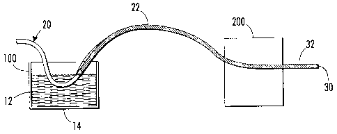
[0029] FIG. I is a schematic diagram showing the process of coating a
substrate
(e.g. a wire) of the present disclosure.
[0030] FIG. 2 is a cross-sectional view of a wire having a palladium layer
and an
overcoat layer atop the palladium layer.
[0031] FIG. 3 is a picture of a copper wire with a palladium coating.
[0032] FIG. 4 is a diagram of a first embodiment of a TFT that can have a
component formed from a palladium precursor composition.
[0033] FIG. 5 is a diagram of a second embodiment of a TFT that can have a
component formed from a palladium precursor composition.
[0034] FIG. 6 is a diagram of a third embodiment of a TFT that can have a
component formed from a palladium precursor composition.
[0036] FIG. 7 is a diagram of a fourth embodiment of a TFT that can have a
component formed from a palladium precursor composition.
[0036] FIG. 8 is a cross-sectional view of an exemplary photovoltaic device
that
can have a component formed from a palladium precursor composition,
DETAILED DESCRIPTION
[0037] A more complete understanding of the components, processes and
apparatuses disclosed herein can be obtained by reference to the accompanying
drawings. These figures are merely schematic representations based on
convenience and the ease of demonstrating the present disclosure, and are,
bb
CA 02778819 2012-05-30
therefore, not intended to indicate relative size and dimensions of the
devices or
components thereof and/or to define or limit the scope of the exemplary
embodiments.
[0038] Although specific terms are used in the following description for
the
sake of clarity, these terms are intended to refer only to the particular
structure of
the embodiments selected for illustration in the drawings, and are not
intended to
define or limit the scope of the disclosure. In the drawings and the following
description below, it is to be understood that like numeric designations refer
to
components of like function.
[0039] The term "room temperature" refers to a temperature of about 23 C.
[0040] The modifier "about" used in connection with a quantity is inclusive
of
the stated value and has the meaning dictated by the context (for example, it
includes at least the degree of error associated with the measurement of the
particular quantity). When used in the context of a range, the modifier
"about"
should also be considered as disclosing the range defined by the absolute
values
of the two endpoints. For example, the range "from about 2 to about 4" also
discloses the range "from 2 to 4."
[0041] The use of the singular terms "a", "an", and "the" should be
construed
to include plural referents as well, unless clearly indicated otherwise by the
context. Put another way, these singular terms should be construed as "at
least
one".
[0042] The present disclosure relates to palladium precursor compositions
which can be used with liquid-based deposition processes to make a palladium
layer on an object or a substrate. The palladium precursor compositions of the
present invention comprise a palladium salt and an organoamine, and are
substantially free of water. In other embodiments, the palladium precursor
compositions of the present disclosure are substantially free of water and
substantially free of reducing agent. In some embodiments, the organoamine
functions as both a complexing agent and a solvent. In other embodiments, the
organoamine functions as a complexing agent only, and the palladium precursor
composition can further comprise a second organic solvent. In specific
embodiments, the organoamine functions as a complexing agent only, and the
palladium precursor composition can further comprise a second organic solvent
which is immiscible with water. In other specific embodiments, the organoamine
6
CA 02778819 2012-05-30
functions as both a complexing agent and a solvent, and the palladium
precursor
composition can further comprise a second organic solvent. These precursor
compositions can be processed into palladium layers with high conductivity and
good adhesion at low temperatures. In particular embodiments, the palladium
precursor compositions consist essentially of the palladium salt and at least
one
organoamine. In other particular embodiments, the palladium precursor
compositions consist essentially of the palladium salt, at least one
organoamine,
and a water immiscible organic solvent.
[0043] The palladium salt may be selected from the group consisting of
palladium carboxylate, palladium chloride, palladium nitrate, palladium
sulfate,
palladium iodide, palladium cyanide, ethylenediamine palladium chloride,
tetraaminepalladium bromide, bis(acetylacetonato) palladium, diamine dinitro
palladium, or mixtures thereof.
[0044] In some embodiments, the palladium salt is a palladium carboxylate
having a general structure of Pd(00CR1)),(00CR2)2..x, wherein R1 and R2 are
independently selected from hydrogen, alkyl having 1 to 11 carbon atoms,
alkenyl
having 2 to about 13 carbon atoms, and alkynyl having 2 to about 13 carbon
atoms. Hydrogen atoms on R1 or R2 may be substituted with another functional
group such as -CHO, -OH, halogen, and the like. In specific embodiments, the
palladium carboxylate is palladium acetate, Pd(O-CO-CH3)2. The number x can
be any number from 0 to 2, for example, 0, 0.01, 0.1 ,1, 1.5, 1.57, 2.0, and
the
like. In preferred embodiments, the palladium salt is a palladium carboxylate.
[0045] The term "alkyl" refers to a radical composed entirely of carbon
atoms
and hydrogen atoms which is fully saturated and of the formula -CnH2ni-1. The
alkyl radical may be linear, branched, or cyclic.
[0046] The term "alkenyl" refers to a radical composed entirely of carbon
atoms and hydrogen atoms which contains at least one carbon-carbon double
bond. An alkenyl radical may be linear or branched. Aromatic rings are not
considered to be alkenyl.
[0047] The term "alkynyl" refers to a radical composed entirely of carbon
atoms and hydrogen atoms which contains at least one carbon-carbon triple
bond.
[0048] It should be noted that the palladium salt is a molecular compound.
Pd-Pd bonds may be present in the molecular compound. However, the
7
CA 02778819 2012-05-30
palladium salt should not be considered to be a nanoparticle or similar
material.
The palladium atom in the salt is not zero valent, while palladium atoms are
zero
valent in the nanoparticle form.
[0049] The organoamine may function as a complexing agent. Generally, the
organoamine may be any primary, secondary, or tertiary amine. The
organoamine can also be a monoamine, diamine, or polyamine. Combinations of
more than one organoamine are also contemplated. More specifically, the
organoamine may contain one, two, or more amine groups of Formula (I):
¨A--N¨C--
Formula (I)
wherein A, B, and C are independently selected from hydrogen and an organic
group, and at least one is an organic group. When the tertiary amine contains
more than one such amine group, the nitrogen atoms are not directly bonded to
each other. An organic group contains at least one carbon atom. Exemplary
organic groups include alkyl, aryl, substituted alkyl, and substituted aryl.
Any two
of organic groups A, B and C can form a cyclic structure.
[0050] The term "aryl" refers to an aromatic radical composed entirely of
carbon atoms and hydrogen atoms. When aryl is described in connection with a
numerical range of carbon atoms, it should not be construed as including
substituted aromatic radicals. For example, the phrase "aryl containing from 6
to
carbon atoms" should be construed as referring to a phenyl group (6 carbon
atoms) or a naphthyl group (10 carbon atoms) only, and should not be construed
as including a methylphenyl group (7 carbon atoms).
[0051] The term "substituted" refers to at least one hydrogen atom on the
named radical being substituted with another functional group, such as
halogen,
hydroxyl, mercapto (-SH), -CN, -NO2, -COON, and -S03H. An exemplary
substituted alkyl group is a perhaloalkyl group, wherein one or more hydrogen
atoms in an alkyl group are replaced with halogen atoms, such as fluorine,
chlorine, iodine, and bromine. Besides the aforementioned functional groups,
an
aryl or heteroaryl group may also be substituted with alkyl or alkoxy.
Exemplary
substituted aryl groups include methylphenyl and methoxyphenyl.
8
CA 02778819 2012-05-30
[0052] Some specific examples of organoamines include ethylamine,
propylamine, butylamine, pentylamine, hexylamine, heptylamine, octylamine,
nonylamine, decylamine, undecylamine, dodecylamine, tridecylamine,
tetradecylamine, hexadecylamine, diaminobutane,
diaminopentane,
diaminohexane, diaminoheptane, diaminooctane,
dianninononane,
diaminodecane, dipropylamine, dibutylamine, dipentylamine, dihexylamine,
diheptylamine, dioctylamine, dinonylamine, didecylamine, methylpropylamine,
ethylpropylamine, propylbutylamine, ethylbutylamine,
ethylpentylamine,
propylpentylamine, butylpentylamine, triethylamine, tributylamine, and
trihexylamine.
[0053] In
more specific embodiments, the organoamine(s) present in the
palladium precursor composition is immiscible in water.
Generally, water
immiscible organoamines contain at least 8 carbon atoms per amine group. In
particular embodiments, the organoamine has only one nitrogen atom (i.e. a
monoamine).
Exemplary water immiscible organoamines include primary
aliphatic amines of the formula NH2-R3, where R3 is alkyl having from 8 to
about
18 carbon atoms, especially those where the R3 is a linear alkyl chain. Some
secondary aliphatic amines are also water immiscible, such as those of the
formula NHR4R5, where R4 and R5 are independently alkyl having from 4 to about
18 carbon atoms. Some tertiary aliphatic amines are also water immiscible,
such
as those of the formula NR6R7R8, where R6, R7, and R8 are independently alkyl
having from 3 to about 18 carbon atoms.
[0054]
Examples of water immiscible organoamines include octylamine,
nonylamine, decylamine, undecylamine, dodecylamine, tridecylamine,
tetradecylamine, hexadecylamine, dipentylamine, dihexylamine, diheptylamine,
dioctylamine, dinonylamine, didecylamine, propylpentylamine, butylpentylamine,
tributylamine, and trihexylamine.
[0055] In
embodiments, the organoamine also functions as a solvent, with
the palladium salt being "dissolved" in the organoamine. The organoamine
should thus be in the liquid phase. Due to the different melting points for
various
organoamines, the temperature of the palladium precursor composition may be
greater than room temperature. For example, dodecylamine has a melting point
of 28-30 C, hexadecylamine has a melting point of 43-46 C, and octadecylamine
has a melting point of 53 C. In some embodiments, the organoamine has a
9
CA 02778819 2012-05-30
. ,
melting point less than 50 degree C, or a melting point of less than 40 degree
C,
including a melting point less than room temperature. In other words, the
organoamine is a liquid at room temperature. Some examples of organoamines
that are liquid at room temperature include octylamine (mp=-1 C),
diaminopropane (mp=-12 C), and tripropylamine (mp=-94 C). The liquid phase /
low melting point is important to achieve a uniform palladium layer. After
liquid
depositing the precursor composition, an amorphous layer will be formed if an
organoamine with a low melting point is used. On the other hand, an
organoamine with a high melting point will crystallize out after deposition of
the
precursor composition, which may cause high surface roughness and holes in the
final palladiumlayer. In embodiments, the temperature of the palladium
precursor
composition may be from room temperature up to about 80 C. This temperature
may occur with no external heat source, for example due to an exothermal
reaction between the palladium salt and the organoamine.
[0056] In some embodiments, the organoamine is not an amino acid
compound. In other words, with reference to Formula (I), none of A, B, or C
are
substituted with a ¨COOH group. In some other embodiments, the organoamine
can be an amino acid compound (i.e. at least one of A, B, and C is substituted
with ¨COOH).
[0057] In more specific embodiments, the organoamine is a primary
monoamine, i.e. a compound of the formula NH2-R3, where R3 is alkyl having
from about 2 to about 18 carbon atoms, including from about 5 to about 14
carbon atoms, or from 8 to about 18 carbon atoms.
[0058] Without being limited by theory, it is believed that the
palladium salt
and the organoamine form a palladium amine complex. This is usually evidenced
by a color change. For example, palladium acetate is a reddish solution in
toluene, but when an organoamine such as octylamine is added, the solution
changes into a light yellow color. The palladium amine complex helps to
dissolve
the palladium salt, permitting high loading of the salt, and as a result, a
high
palladium content in the precursor composition. In embodiments, the palladium
amine complex is dissolved, and the resulting precursor composition is a clear
solution. It should be noted that the composition may also comprise non-
complexed palladium salt molecules. In specific embodiments, the composition
CA 02778819 2012-05-30
. .
comprises the palladium amine complex and an excess amount of the
organoamine in non-complexed form.
[0059] In other specific embodiments, the palladium amine complex
is formed
from a monoamine. In particular, the monoamine may be a primary alkyl
monoamine of the formula NH2-R3, where R3 is alkyl having at least 8 carbon
atoms.
[0060] The palladium and organoamine in the precursor composition
form a
complex. It should be noted that palladium is sometimes used as a catalyst in
organic synthesis. When an organic synthesis reaction contains an organoamine
reagent, a palladium organoamine complex might be formed in an organic
reaction. This differs from the present disclosure in several aspects. First,
the
palladium in a synthesis reaction functions as a catalyst, while the palladium
in
the present precursor composition provides a metal source for a palladium
layer,
and does not act as a catalyst. Second, the organoamine in a synthesis
reaction
functions as a reactant, while the organoamine in the precursor composition
functions as a complexing agent and/or solvent. Third, palladium is used in a
catalytic amount in those synthesis reactions, while palladium salt is merely
one
of the dominant components of the precursor composition. In general, here the
precursor composition is a non-catalytic composition. Stated differently, the
palladium amine complex is not used in forming a product from two reactants.
The term "non-catalytic" refers to the fact that the palladium in the
palladium
precursor composition does not function as a catalyst. This can be seen in
that
the organoamine does not become part of a third compound in the precursor
composition. In other words, the palladium precursor composition does not
contain any compounds which become covalently coupled to the organoamine.
[0061] In embodiments, the molar ratio of the organoamine to the
palladium
salt is from about 1:1 to about 10:1. In more specific embodiments, the molar
ratio of organoamine to palladium salt is from about 1:1 to about 5:1, or from
about 2:1 to about 5:1, or from about 2:1 to about 3:1. In some embodiments,
the
molar ratio of the organoamine to the palladium salt is at least 2:1 to ensure
good
dissolution of the palladium salt in the organoamine.
[0062] In other specific embodiments, particular combinations of
palladium
salt and organoamine are contemplated. In these combinations, the total number
of carbon atoms in the palladium salt and organoamine are combined, and their
11
CA 02778819 2012-05-30
. =
total is 10 or higher. For example, if the palladium salt is palladium
carboxylate
Pd(00CR1)(00CR2)2..x, and the organoamine is octylamine H2N-R3, then the
total number of carbon atoms is the carbon atoms in R3 + carbon atoms in R1
times X + carbon atoms in R2 time (2-X) +2. As a specific example, if the
palladium salt is palladium acetate Pd(OCOCH3)2 and the organoamine is
octylamine, then the total number of carbon atoms is 12, four from the acetate
and eight from the organoamine. The total number is based on the chemical
formulae for the palladium salt and organoamine. The total number does not
change with differences in the relative amounts of the palladium salt and
organoamine, and is not related to the number of moles or the weight
percentages of the two ingredients. In other embodiments, the total number of
carbon atoms in the palladium salt and organoamine is at least 10, or at least
11,
or at least 12.
[0063] In embodiments, another organic solvent which is
immiscible with
water can be included, or in other words a second water immiscible organic
solvent can be used. When a given organic solvent is mixed with water at about
equal amounts by volume, if a phase separation is detected (either visually or
by
instruments such as light scattering or refractive index) after settling, the
solvent
is considered to be water immiscible. The palladium salt, the organoamine, and
the resulting palladium amine complex should be soluble in this second
solvent.
For example, at least 0.5 wt% of the amount of the given component added to
the
second solvent should dissolve, including at least 1 wt%, or at least 10 wt%
of the
amount added. The non-soluble portion can be removed from the precursor
composition by, for example, filtration.
[0064] Any suitable water immiscible organic solvent can be used
for the
second solvent. In some embodiments, the second organic solvent may be a
hydrocarbon solvent, for example a substituted hydrocarbon or an aromatic
hydrocarbon solvent. Specifically, the hydrocarbon solvent has at least 6
carbon
atoms, from 6 to about 25 carbon atoms. Exemplary solvents include toluene,
xylene, mesitylene, ethylbenzene, diethylbenzene, trimethyl benzene, methyl
ethylbenzene, tetrahydronaphthalene, chlorobenzene, dichlorobenzene,
trichlorobenzene, chlorotoluene, and the like, or mixtures thereof. In other
embodiments, the second organic solvent is a ketone, ester, ether, and the
like.
Exemplary solvents include methyl isobutyl ketone, methyl benzoate, benzyl
12
CA 02778819 2012-05-30
benzoate, anisole, cyclohexanone, acetophenone, and the like. In
some
embodiments, the second organic solvent has a boiling point at least 80 C,
including at least 100 C. In some specific embodiments, the second solvent has
a high boiling point at least 150 C.
[0065] In
particular embodiments, the palladium precursor composition should
not contain any water. In other words, the palladium precursor composition
fails
to include water, or is substantially free of water. However, it should be
noted
that these phrases do not require an absolute absence of water. Some residual
water may be present in the precursor composition from the various ingredients
or from ambient/atmospheric conditions. For example, octylamine is typically
sold with a specification of maximum 0.1 wt% water content, or tributylamine
is
typically sold with a specification of maximum 0.3 wt% water content. These
amounts of water should be considered to be residual and precursor
compositions containing such amounts of water should be considered
substantially free of water.
[0066] In
some other embodiments, water and/or a water miscible solvent may
be present in the palladium precursor composition. However, the amount of
water and/or water miscible solvent (by weight) is in some embodiments less
than the amount of organoamine. Exemplary water miscible solvents include
alcohols such as methanol, ethanol, propanol, and butanol; glycols, acetone,
tetrahydrofuran (THF), dichloromethane, ethyl acetate, dimethylformamide
(DMF), dimethyl sulfoxide (DMSO), acetic acid, acetonitrile, and dioxane. Any
suitable concentration of the water and/or water miscible solvent(s) may be
present.
[0067] The
palladium salt typically makes up from about 1 to about 50 weight
percent (wt%) of the precursor composition. In more specific embodiments, the
palladium salt makes up from about 5 wt% to about 30 wt% of the precursor
composition.
[0068] The
precursor composition can further include another metal species,
for example silver (Ag), gold (Au), copper (Cu), nickel (Ni), rhodium (Rh),
cobalt
(Co), zinc (Zn), platinum (Pt), and the like. The other metal species may be
introduced as another starting ingredient, for example in the form of a metal
salt.
For example, silver acetate can be used in combination with palladium acetate
to
form a Ag-Pd alloy. The additional metal salt in the composition can be
present in
13
CA 02778819 2012-05-30
. ,
an amount of, for example, from about 0.1 wt% to about 40 wt%, including from
about 1 wt% to about 20 wt% of the precursor composition. However, the
additional metal salt should be less than the amount of the palladium salt.
[0069] The palladium precursor composition has a surface tension
of less than
33 mN/m, including less than 30 mN/m, or less than 28 mN/m, or for example
from about 23 mN/m to about 30 mN/m. This low surface tension enables a
uniform coating of palladium to be formed on the substrate. The selection of a
suitable organoamine or second water-immiscible organic solvent provides the
desired surface tension. The palladium precursor composition has a viscosity
from about 0.8 to about 100 cps, including from about 0.8 to about 50 cps, or
about 2 to about 30 cps.
[0070] In certain embodiments, the palladium precursor
composition does not
contain a reducing agent, or is substantially free of reducing agent. Some
examples of such reducing agents include formic acid and formic acid salts or
esters, hypophosphites, hydrazines, ammonium compounds, amine borane
compounds, alkali metal borohydrides, oxalic acid, alkali or alkaline earth
sulfites,
and the like.
[0071] The palladium precursor composition can be used to apply a
palladium
coating or layer onto any substrate or object via solution deposition. The
palladium precursor composition can be solution deposited upon the substrate.
"Solution depositing" and "solution processing" refer to a process where a
liquid is
deposited upon the substrate to form a structure. This is in contrast to
vacuum
depositing processes. The present processes for forming a palladium structure
are also different from other solution-based processes, for example
electroplating, which requires a plate to remain immersed in a solution and
also
requires exposure to an electric current to form a metal coating on the plate.
The
present processes also offer several advantages compared to electroless
plating.
In electroless plating, the deposition of the palladium is slow, so that the
overall
plating process takes much longer than the solution deposition processes of
the
present disclosure. Electroless plating also generates a great deal of waste
due
to residual metal present in the solution. Electroless plating baths or
solutions
also often contain a reducing agent. In addition, the present processes allow
for
fine control of where the palladium is deposited for example by inkjet
printing. In
other words, it is easy to form a patterned palladium structure in a discrete
14
CA 02778819 2012-05-30
. .
location using the present processes. In contrast, metal deposition in
electroless
plating occurs over all surfaces which are immersed in the solution. Masking
surfaces which are not to be plated is a complex and time-consuming procedure.
However, the present processes can be used in combination with electroplating
or electroless plating if needed. For example, the palladium layer formed
using
the present processes can be used as the base layer for electroplating.
Electroless plating palladium or other metals such as copper can be further
performed on top of the palladium layer formed with the present processes, for
example to increase the thickness of a conductive layer, since palladium is a
good seeding layer for electroless plating.
[0072] Exemplary solution deposition processes include dip
coating, spin
coating, spray coating, flexographic printing, offset printing, or inkjet
printing
(where the palladium precursor composition is ejected onto the substrate by an
inkjet printhead). Certain processes involve solution depositing the substrate
with
the palladium precursor composition to form a structure or film on the
substrate.
In embodiments, the structure or film has a thickness of from about 10
nanometers to about 50 micrometers, including from about 10 nm to about 30
micrometers, or from about 50 nm to about 5 micrometers, or from about 80 nm
to about 1 micrometer.
[0073] The palladium precursor composition which was previously
deposited
is then heated to form the palladium layer on the substrate. The heating
causes
the palladium amine complex or palladium salt to thermally decompose to form a
solid palladium layer. In contrast, in electroless plating, the palladium salt
or
complex is chemically reduced to palladium. The heating may be performed at a
temperature of from about 80 C to about 350 C. In other embodiments, the
heating is performed at a temperature of above 100 C, or from about 120 C to
about 300 C, or from about 150 C to about 250 C, or a temperature below
200 C, or a temperature below 150 C. Regardless of the substrate used, the
heating temperature is desirably one that does not cause adverse changes in
the
properties of any previously deposited layer(s) or the substrate (whether a
single
layer substrate or multilayer substrate). The heating may be performed for a
period of up to 30 minutes, and could be for a period as short as 0.1 seconds
depending on the size of the palladium layer and the heating method. The
heating can be performed in air, in an inert atmosphere (for example, under
CA 02778819 2012-05-30
nitrogen or argon), or in a reducing atmosphere (for example, under nitrogen
containing from 1 to about 20 percent by volume hydrogen). The heating can
also
be performed under normal atmospheric pressure or at a reduced pressure of,
for
example, from about 1000 millibars to about 0.01 millibars. Examples of
heating
techniques may include thermal heating (for example, a hot plate, an oven, and
a
burner), infra-red ("IR") radiation, a laser beam, flash light, microwave
radiation,
or UV radiation, or a combination thereof.
[0074] During the heating, in some embodiments, at least a portion of the
palladium organoamine complex first form palladium nanoparticles in-situ.
These
palladium nanoparticles subsequently coalesce into a continuous and uniform
palladium layer. This intermediate step where palladium nanoparticles are
formed
will enhance uniformity of the final palladium film. This is different from a
conventional electroless plating process, where the palladium salt deposits
into a
palladium layer directly without going through an intermediate nanoparticle
form.
In further embodiments, a majority of the palladium organoamine complex forms
palladium nanoparticles in-situ. The formation of palladium nanoparticles is
evidenced by the color change of the deposited palladium organoamine complex
upon heating. A black color is often observed prior to the formation of the
silvery
metallic palladium layer, indicating that a palladium nanoparticle
intermediate
was formed during the heating step.
[0075] It should be noted that when the palladium precursor composition is
heated to form the palladium layer, the temperature of the precursor
composition
is increased above the temperature of the precursor composition during the
solution deposition. As previously discussed, the temperature of the precursor
composition may be greater than room temperature to ensure the organoamine is
in the liquid phase during the solution deposition.
[0076] The deposition processes described herein can also be repeated to
build up a thicker palladium layer on the object. For example, in embodiments,
the thickness of the final layer may also be from about 10 nanometers to about
50 micrometers, or from about 50 nanometers to about 30 micrometers, or from
about 50 nm to about 5 micrometers, or from about 80 nm to about 1 micrometer.
In this regard, multiple solution deposition steps may be performed, with one
subsequent heating to form the final layer. Alternatively, the steps of
solution
16
CA 02778819 2012-05-30
deposition and heating can be repeated multiple times to build a thick layer
out of
several thinner layers.
[0077] Prior to heating, the structure or film containing the palladium
salt or
palladium amine complex may be electrically insulating or have very low
electrical
conductivity. Heating results in an electrically conductive layer of
palladium. The
conductivity of the palladium layer produced by heating is, for example, more
than about 100 Siemens/centimeter ("S/cm"), more than about 1000 S/cm, more
than about 2,000 S/cm, more than about 5,000 S/cm, or more than about 10,000
S/cm or more than 50,000 S/cm.
[0078] In some embodiments, prior to heating, the structure containing the
palladium salt or palladium amine complex is amorphous. In some specific
embodiments, the palladium organoamine complex remains in the liquid phase
prior to heating.
[0079] In other embodiments, the palladium layer is not conductive.
Although
heating causes the decomposition of the palladium complex into palladium, due
to the presence of other ions (from the salt) or a residual amount of the
organoamine and its decomposed form, or due to the presence of insulative
additives in the precursor composition such as polymers, the palladium layer
may
not necessarily be conductive. However, the palladium layer does have a shiny
metallic white color.
[0080] In some embodiments, reducing agents may not be needed to prepare
and obtain the palladium layer on the object or substrate. Thus, such reducing
agents are not present in the palladium precursor composition and are not
separately added as an additional processing step.
[0081] In particular embodiments, the palladium precursor composition
consists essentially of one or more palladium salts and one or more
organoamines. The precursor composition has the basic characteristic of being
solution-processable. The precursor composition does not contain a reducing
agent. In specific embodiments, the organoamine is a primary monoamine.
[0082] It is specifically contemplated that the processes used herein can
be
used for coating a wire. It should be noted that any wire can be coated with
the
palladium precursor composition, regardless of the diameter, shape, or length
of
the wire. Both organic materials (e.g. plastic) and inorganic materials (e.g.
copper) can be used as the substrate for the wire. The wire may be bare (i.e.
17
CA 02778819 2014-07-31
=
uncovered with other layers) or may be insulated by the addition of other
layers
around a core. The wire may be single-stranded (i.e. solid), multiple
stranded,
and/or twisted. Exemplary inorganic materials include metals such as copper,
aluminum, tungsten, zinc oxide, silicon, and the like. Exemplary plastic wires
include
wires made from polyimide, polyester, polyamide (NylorTm), polycarbonate,
polyethylene, polyacrylate, and the like.
[0083] Optionally, a receiving layer can be applied prior to drawing the
object (i.e.
wire) through the palladium precursor composition. The receiving layer may
enhance
the adhesion of the precursor composition on the object. Any suitable
receiving layer
can be used. Exemplary receiving layers can be formed from, for example, a
silane,
especially a silane comprising an amino group.
[0084] If desired, additional layers can be applied on top of the palladium
layer
(the additional layers may be referred to as overcoat layers). Any layer known
in the
art may be applied, particularly materials with good scratch resistance. In
embodiments, materials that can be used to form an overcoat layer include an
epoxy
resin, a polyurethane, a phenol resin, a melamine resin, a polysiloxane, a
poly(silsesquioxane), and the like. Polysiloxane and poly(silsesquioxane)
precursors
(for example sol-gel approach) can be used to from a highly crosslinked
polysiloxane
or poly(silsesquioxane) overcoat layer. In some specific embodiments, the
overcoat
layer is a crosslinked polysiloxane, a crosslinked poly(silsesquioxane), or a
crosslinked layer comprising poly(vinylphenol) and a melamine-formaldehyde
resin.The thickness of the overcoat layer may be for example from about 10 nm
to
about 10 micrometers, including from about 10 nm to about 5 micrometers, or
from
about 50 nm to about 1 micrometer. In embodiments, the overcoat layer is
transparent to visible light. In other words, the overcoat layer is colorless.
This will
ensure the visibility of the palladium layer.
[0085] FIG. us a schematic diagram illustrating the processes described
herein.
In step 100, a palladium precursor coating solution 12 is presented in a
vessel 14. A
wire 20 is drawn through the coating solution to form a coating 22 on the
wire. Note
that this allows for continuous production of the wire. Next in step 200, the
coating
22 is annealed by exposure to heat. The result is a wire 30 having a palladium
layer
32. The original wire 20 serves as a substrate upon which the palladium layer
is
located.
18
CA 02778819 2012-05-30
[0086] FIG. 2 is a cross-sectional view of the final wire 30. At the center
is the
original wire 20. As noted above, this original wire 20 may comprise a core 21
and other layers prior to receiving the palladium layer. For example, the
original
wire may include a receiving layer 23. The palladium layer 32 covers the wire
20.
An overcoat layer 34 may surround the palladium layer 32.
[0087] It may be desirable to clean the wire prior to drawing the wire
through
the palladium precursor composition. This can be done by, for example, wiping
the wire with isopropanol or using a plasma treatment on the surface of the
wire.
This will aid in maintaining a uniform coating.
[0088] The palladium precursor composition may also be useful in forming
electrically conductive elements such as electrodes, conductive lines,
conductive
pads, conductive tracks, circuits, pathways, channels, conductive coatings,
conductive films, and the like in electronic devices such as thin film
transistors
(TFTs), organic light emitting diodes (OLED), radio frequency identification
(RFID) tags, photovoltaic, and other electronic devices that include
conductive
elements or components.
[0089] FIGs. 4-7 illustrate some different configurations of thin film
transistors.
The palladium precursor composition could be used, for example, to form any of
the electrodes (gate, source, drain) in the transistor.
[0090] FIG. 4 illustrates a bottom-gate bottom-contact TFT configuration
according to the present disclosure. The TFT 310 comprises a substrate 316 in
contact with the gate electrode 318 and a gate dielectric layer 314. The gate
electrode 318 is depicted here atop the substrate 316, but the gate electrode
could also be located in a depression within the substrate. It is important
that the
gate dielectric layer 314 separates the gate electrode 318 from the source
electrode 320, drain electrode 322, and the semiconducting layer 312. The
semiconducting layer 312 runs between the source and drain electrodes 320 and
322. The semiconductor has a channel length between the source and drain
electrodes 320 and 322.
[0091] FIG. 5 illustrates a bottom-gate top-contact TFT configuration
according to the present disclosure. The TFT 330 comprises a substrate 336 in
contact with the gate electrode 338 and a gate dielectric layer 334. The
semiconducting layer 332 is placed on top of the gate dielectric layer 334 and
separates it from the source and drain electrodes 340 and 342.
19
CA 02778819 2012-05-30
[0092] FIG. 6 illustrates a bottom-gate bottom-contact TFT configuration
according to the present disclosure. The TFT 350 comprises a substrate 356
which also acts as the gate electrode and is in contact with a gate dielectric
layer
354. The source electrode 360, drain electrode 362, and semiconducting layer
352 are located atop the gate dielectric layer 354.
[0093] FIG. 7 illustrates a top-gate top-contact TFT configuration
according to
the present disclosure. The TFT 370 comprises a substrate 376 in contact with
the source electrode 380, drain electrode 382, and the semiconducting layer
372.
The semiconducting layer 372 between the source and drain electrodes 380 and
382. The gate dielectric layer 374 is on top of the semiconducting layer 372.
The
gate electrode 378 is on top of the gate dielectric layer 374 and does not
contact
the semiconducting layer 372.
[0094] A thin film transistor generally includes a substrate, a dielectric
layer,
and a semiconducting layer in addition to the source electrode, drain
electrode,
and optional gate electrode.
[0095] The substrate may be composed of materials including but not limited
to silicon, glass plate, plastic film or sheet, and various metals. For
structurally
flexible devices, plastic substrate, such as for example polyester,
polycarbonate,
polyimide sheets and the like may be preferred. The thickness of the substrate
may be from about 10 micrometers to over 10 millimeters with an exemplary
thickness being from about 50 to about 100 micrometers, especially for a
flexible
plastic substrate and from about 0.5 to about 10 millimeters for a rigid
substrate
such as glass or silicon.
[0096] The dielectric layer generally can be an inorganic material film, an
organic polymer film, or an organic-inorganic composite film. Examples of
inorganic materials suitable as the dielectric layer include silicon oxide,
silicon
nitride, aluminum oxide, barium titanate, barium zirconium titanate and the
like.
Examples of suitable organic polymers include polyesters, polycarbonates,
poly(vinyl phenol), polyimides, polystyrene, polynnethacrylates,
polyacrylates,
epoxy resin and the like. The thickness of the dielectric layer depends on the
dielectric constant of the material used and can be, for example, from about
10
nanometers to about 500 nanometers. The dielectric layer may have a
conductivity that is, for example, less than about 10-12 Siemens per
centimeter
CA 02778819 2012-05-30
. ,
(S/cm). The dielectric layer is formed using conventional processes known in
the
art, including those processes described in forming the gate electrode.
[0097]
The dielectric layer may be surface modified with a surface modifier.
Exemplary surface modifiers include organosilanes such as
hexamethyldisilazane (HMDS), octyltrichlorosilane
(OTS-8),
octadecyltrichlorosilane (ODTS-18), and phenyltrichlorosilane (PTS). The
semiconducting layer can be directly contacted with this modified dielectric
layer
surface. The contact may be complete or partial. This surface modification can
also be considered as forming an interfacial layer between the dielectric
layer and
the semiconducting layer.
[0098] The semiconducting layer generally is made from an organic
semiconducting material. Examples of organic semiconductors include but are
not limited to acenes, such as anthracene, tetracene, pentacene, and
substituted
pentacenes, perylenes, fullerenes, oligothiophenes, polythiophenes and their
substituted derivatives, polypyrrole, poly-p-phenylenes, poly-p-
phenylvinylidenes,
naphthalenedicarboxylic dianhydrides, naphthalene-bisimides, polynaphthalenes,
phthalocyanines such as copper phthalocyanines or zinc phthalocyanines and
their substituted derivatives. The semiconductor may also be an inorganic
semiconductor such as ZnO, ZnS, silicon nanowires, and the like.
[0099]
In specific embodiments, the semiconductors are polythiophenes.
Polythiophenes include, for example, regioregular and regiorandom poly(3-
alkylthiophene)s, polythiophenes comprising substituted and unsubstituted
thienylene groups, polythiophenes comprising optionally substituted thieno[3,2-
b]thiophene and/or optionally substituted thieno[2,3-b]thiophene groups,
polythiophenes comprising fused-ring aromatic groups, polythiophenes
comprising heteroatom-containing fused-ring aromatic groups, and
polythiophenes comprising non-thiophene based aromatic groups such as
phenylene, fluorene, furan, and the like.
[0100] The semiconducting layer is from about 5 nanometers to about 1000
nanometers deep, including from about 20 to about 100 nanometers in depth. In
certain configurations, such as the configurations shown in FIG. 3 and FIG. 6,
the
semiconducting layer completely covers the source and drain electrodes. The
semiconducting layer has a channel length defined by the distance between the
source and drain electrodes.
21
CA 02778819 2012-05-30
, .
[0101] The semiconducting layer can be formed by molecular beam
deposition, vacuum evaporation, sublimation, spin-on coating, dip coating,
printing (e.g., inkjet printing, screen printing, stencil printing,
microcontact
printing, flexographic printing), and other conventional processes known in
the
art, including those processes described in forming the gate electrode.
[0102] Regarding electrical performance characteristics, the organic
semiconductor usually has a conductivity in the range of 10-8 to 10-4 S/cm.
Various dopants known in the art may also be added to change the conductivity.
The organic semiconductor can be either a p-type or n-type semiconductor. For
p-type, the semiconductor usually has an energy level (HOMO level) of higher
than 4.5 eV. In specific embodiments, the p-type semiconductor has a HOMO
level of about 5.1 eV. For n-type, the semiconductor usually has a energy
level
(LUMO level) of lower than 4.5 eV. In specific embodiments, the n-type
semiconductor has a LUMO level of about 4.0 eV. In specific embodiments, the
semiconductor is a p-type semiconductor. In specific embodiments, the organic
semiconductor is a polythiophene. Polythiophenes generally have a HOMO level
of from about 4.7 eV to about 5.5 eV.
[0103]
The source, drain, and optional gate electrodes may be made from
other electrically conductive materials as well. They can be for example, a
thin
metal film, a conducting polymer film, a conducting film made from conducting
ink
or paste, or in the case of the gate electrode the substrate itself, for
example
heavily doped silicon. Other examples of electrode materials include but are
not
restricted to aluminum, gold, silver, chromium, zinc, indium, conductive metal
oxides such as zinc-gallium oxide, indium tin oxide, indium-antimony oxide,
conductive polymers such as polystyrene sulfonate-doped poly(3,4-
ethylenedioxythiophene) (PSS-PEDOT), and conducting ink/paste comprised of
carbon black/graphite. The electrodes can be prepared by vacuum evaporation,
sputtering of metals or conductive metal oxides, conventional lithography and
etching, chemical vapor deposition, spin coating, casting or printing, or
other
deposition processes. The thickness of the gate electrode ranges for example
from about 10 to about 200 nanometers for metal films and from about 1 to
about
micrometers for conductive polymers.
Typical thicknesses of source and
drain electrodes are, for example, from about 40 nanometers to about 1
22
CA 02778819 2012-05-30
micrometer, including more specific thicknesses of from about 100 to about 400
nanometers.
[0104] If desired, a barrier layer may also be deposited on top of the TFT
to
protect it from environmental conditions, such as light, oxygen and moisture,
etc.
which can degrade its electrical properties. Such barrier layers are known in
the
art and may simply consist of polymers.
[0105] The various components of the TFT may be deposited upon the
substrate in any order. Generally, however, the gate electrode and the
semiconducting layer should both be in contact with the gate dielectric layer.
In
addition, the source and drain electrodes should both be in contact with the
semiconducting layer. The phrase "in any order" includes sequential and
simultaneous formation. For example, the source electrode and the drain
electrode can be formed simultaneously or sequentially. The term "on" or
"upon"
the substrate refers to the various layers and components with reference to
the
substrate as being the bottom or support for the layers and components which
are on top of it. In other words, all of the components are on the substrate,
even
though they do not all directly contact the substrate. For example, both the
dielectric layer and the semiconducting layer are on the substrate, even
though
one layer is closer to the substrate than the other layer.
[0106] FIG. 8 is a side cross-sectional view of an exemplary photovoltaic
device 700. A substrate 710 is provided. A first electrode, such as anode 720,
is
located upon the substrate 710. A semiconducting layer 740 is then located
upon
the anode 720. In some embodiments, such as the one depicted here, the
semiconducting layer 740 may be made from layers of different materials, shown
here as a first sublayer 742 and a second sublayer 744. The first sublayer 742
is
located closer in distance to the anode 720 than the second sublayer 744. A
junction 745 is formed between the first sublayer 742 and the second sublayer
744. An optional electron blocking layer 730 may be located between the anode
720 and the first sublayer 742, if desired. An electron transporting layer 750
contacts the second sublayer 744 of the semiconducting layer 740. An optional
hole blocking layer 760 is located on the electron transporting layer 750.
Finally,
a second electrode, such as cathode 770, is placed upon the substrate 710 and
on the hole blocking layer 760. The second sublayer 744 of the semiconducting
layer 740 is closer to the cathode 770 than the first sublayer 742. It should
also
23
CA 02778819 2012-05-30
be noted that the anode 720 is located closer to the substrate 710 than
cathode
770.
[0107] Only the substrate 710, anode 720, semiconducting layer 740,
electron
transporting layer 750, and cathode 770 are required to produce a functioning
photovoltaic device. However, the additional layers are also helpful in
obtaining a
highly efficient photovoltaic device. When described in other terms, the
semiconducting layer 740 is located between the anode 720 and the cathode
770. Also, the electron transporting layer 750 is located between the second
sublayer 744 and the cathode 770. The hole blocking layer 760 is located
between the second sublayer 744 and the cathode 770 as well. When both an
electron transporting layer and hole blocking layer are present, the hole
blocking
layer 760 is located between the electron transporting layer 750 and the
cathode
770.
[0108] The substrate 710 of the photovoltaic device supports the other
components of the photovoltaic device. The substrate should also be optically
transparent in at least the NIR range of the spectrum, to allow light to pass
through and contact the semiconducting layer. Generally, the substrate is
composed of materials as previously described for the substrate of a thin film
transistor.
[0109] The anode 720 or cathode 770 may be made from the palladium
precursor composition, or using materials as previously described for the
electrodes of a thin film transistor. The semiconducting layer 740 can be made
using materials as previously described for the electrodes of a thin film
transistor.
[0110] The electron transporting layer 750 is located between the
semiconducting layer 740 and the cathode 770. This layer is generally made
from a material which allows electrons to move efficiently, and may also
absorb
some light wavelengths. Exemplary materials for the electron transporting
layer
include C60 fullerene, [6,6]-phenyl-C61-butyric acid methyl ester (PCBM), C70
fullerene, [6,6]-phenyl-C71-butyric acid methyl ester (PC[70]BM), or any
fullerene
derivative. The electron transporting layer may have a thickness of from about
5
nanometers to about 100 nanometers.
[0111] An electron blocking layer 730 may be present between the anode 720
and the semiconducting bilayer 740. This layer prevents recombination at the
anode by inhibiting the movement of electrons to the anode. Exemplary
24
CA 02778819 2012-05-30
. .
materials include poly(3,4-ethylenedioxythiophene):poly(styrene sulfonic acid)
(PEDOT:PSS), Mo03, and V205. The electron blocking layer may have a
thickness of from about 1 nanometers to about 100 nanometers.
[0112] A hole blocking layer 760 may also be located between the
electron
transporting layer 750 and the cathode 770. Exemplary hole blocking materials
for this layer include bathocuproine (BCP), lithium fluoride, and
bathophenanthroline. The hole blocking layer may have a thickness of from
about 0.1 nanometers to about 100 nanometers.
[0113] The following examples are for purposes of further
illustrating the
present disclosure. The examples are merely illustrative and are not intended
to
limit devices made in accordance with the disclosure to the materials,
conditions,
or process parameters set forth therein.
EXAMPLES
Comparative Example
[0114] Palladium acetate (trimer) was purchased from Alfa Aesar.
0.1 grams
of palladium acetate was added into 0.7 grams toluene. The salt was partially
soluble and displayed an orange-brown color.
Example 1
[0115] Palladium acetate (trimer) was purchased from Alfa Aesar.
0.1 grams
of palladium acetate was added into 0.7 grams toluene. 0.22 grams of
octylamine was then added into the mixture, and the mixture was then shaken.
The insoluble part of the palladium salt was dissolved to form a very stable
light
yellow solution.
Test Results
[0116] The solutions of the Comparative Example and Example 1 were each
spin-coated onto a glass slide to form a film. The solution of Example 1
formed a
uniform film without crystallization or precipitation. In contrast, the
solution of the
Comparative Example formed a non-uniform film with precipitates of the salt
after
spin coating.
CA 02778819 2012-05-30
[0117] After being heated at 200-250 C for a few minutes, the film of Example
1 changed into first a black color, then a shiny metallic color. The palladium
thin
film was measured to be very conductive by two probe measurement having a
conductivity estimated to be around 1.0 x 10⁴S/cm.
Example 2
[0118] A copper wire was dipped into the solution of Example 1 to coat the
surface of the wire with the palladium precursor composition. After being
slowly
pulled out of the solution, the wire was heated at 200 C in an oven for 5
minutes
under reducing gas (4.5 % hydrogen in nitrogen). A shiny metallic white wire
was
obtained, and is seen in FIG. 3. The palladium coating was very robust when
washed with solvents such as isopropyl alcohol (IPA) and toluene, i.e. the
coating
did not dissolve or flake. The palladium coating also resisted damage under
mechanical rubbing.
Example 3
[0119] Palladium acetate (trimer) was purchased from Alfa Aesar. 0.1 grams
of palladium acetate was added into 0.7 grams benzyl benzoate. 0.22 grams of
octylamine was then added into the mixture, and the mixture was then shaken.
The insoluble part of the palladium salt was dissolved to form a very stable
light
yellow solution.
Example 4
[0120] 2.5 grams of palladium acetate was added into 1.5 grams toluene. 6.0
grams of octylamine was then added into the mixture slowly, and the mixture
was
then shaken. The temperature of the mixture increased to about 60-65 degree C
due to the exothermal reaction between palladium acetate and octylamine to
form
palladium organoamine complex. After stirring for 24 hours at room
temperature,
the palladium acetate was completely dissolved to form a very stable light
yellow
solution. The viscosity of the solution was measured to be about 30 cps.
Example 5
[0121] 0.1 grams of palladium acetate was added into 0.25 grams octylamine.
The liquid octylamine functioned as both a complexing agent and a solvent.
After
26
CA 02778819 2012-05-30
, .
being stirred at room temperature, a clear yellow color oil-like paste was
obtained. The paste was painted on a glass slide and annealed at 250 degree C
in an oven. The clear paste turned into a dark paste first, then into a
silvery
metallic palladium layer.
[0122] It will be appreciated that variants of the above-
disclosed and other
features and functions, or alternatives thereof, may be combined into many
other
different systems or applications. Various presently unforeseen or
unanticipated
alternatives, modifications, variations or improvements therein may be
subsequently made by those skilled in the art which are also intended to be
encompassed by the following claims.
27