Note: Descriptions are shown in the official language in which they were submitted.
WO 2011/051146 CA 02778855 2012-04-24
PCT/EP2010/065775
1
MULTI-PORT AMPLIFICATION DEVICE THAT SELF-COMPENSATES
IN THE PRESENCE OF TRAFFIC
The present invention relates to a multi-port amplification device
known by the abbreviation MPA (Multi-Port Amplifier), also called a
distributed-amplification sub-system. This type of device is commonly used in
communication systems using multibeam antennas which have the capacity
to form several wavebeams in various directions. In particular, satellite
communication systems use this type of amplifier to flexibly distribute
several
transmission channels to several output beams.
One of the essential parameters of a multi-port amplifier is the
isolation between the various output pathways which must be sufficient to
guarantee acceptable isolation between the beams generated by the
antenna. The isolation of a first output pathway in relation to a second
output
pathway different from the first is measured by the ratio of the maximum
power of the amplified signal on the first output pathway of the multi-port
amplifier to the residual power present on the second output pathway of the
multi-port amplifier, this residual power being due to the imperfections of
the
system and also to the phenomenon of intermodulation.
A theoretical multi-port amplifier possesses infinite isolation between
each of its output ports, however in practice, the Butler matrices and the
amplification chains used within such an amplifier are not ideal and exhibit
imperfections which may give rise to amplitude and phase errors which
ultimately have an impact on the isolation of each of the output pathways in
relation to the others. This phenomenon has notably all the more impact the
higher the carrier frequency used. In view of these limitations, it is
therefore
necessary to produce a solution making it possible to correct the amplitude
error and phase error and therefore to improve the overall isolation of the
system.
WO 2011/051146 CA 02778855 2012-04-24
PCT/EP2010/065775
2
American patent US7088173 describes a scheme making it possible
to correct the phase imperfections within a multi-port amplifier. The
envisaged solution uses test signals injected at various points of the input
network and measured at various points of the output network so as to
determine the phase errors impacting the amplifiers. This solution makes it
necessary to deactivate part of the amplifiers in order to perform the various
measurements required. This scheme is therefore not suited to the
simultaneous implementation of a communication.
American patent US6006111 and Japanese patent JP2005269043
also describe methods making it possible to compensate for the
imperfections of a distributed-amplification system on the basis of
measurements performed on one or more output pathways but these
schemes use only the measurement of the amplitude without taking the
phase errors into account.
International patent application W02008135753 describes a self-
compensated multi-port amplifier solution comprising 8 input pathways and 8
output pathways. The principle consists in injecting a reference signal on the
first input branch of the device and then measuring the imbalance between
pathways, by virtue of 7 power detectors distributed in the output matrix.
Several feedback loops then act on the attenuators and the phase shifters
placed upstream of the amplifiers so as to minimize the voltage detected at
each of the 7 points.
The scheme described in this patent application uses an iterative method for
adjusting the amplitude and the phase upstream of the amplifiers so as to
converge toward a zero power value on each point of the output matrix where
a power detector is positioned. This method does not seem sufficiently
efficacious to ensure sufficient isolation since the isolation matrix after
compensation appears degraded in comparison with the isolation matrix
before compensation. The result obtained is, in particular, not compatible
with the proper operation of a telecommunications satellite mission.
CA 02778855 2017-01-19
3
Finally, American patent application US20080143562 may also be
cited, which proposes a compensation scheme based on a priori knowledge
of the signal transmitted by modeling its probability density. Such a scheme
is
too restrictive since it is not adaptable to all types of signal, in
particular a
signal modulated by the combination of several simple modulations.
In view of the limitations of the prior art, the present invention
introduces a self-compensated distributed-amplification system with the aim
of minimizing the amplitude error and phase error inherent in the
imperfections
of such a system. This system may make it possible to considerably improve
performance in respect of isolation between output pathways of the device
and operates in the presence of traffic, that is to say without interrupting
the
nominal operation of the communication system implementing an amplifier
according to the invention.
The present invention provides a system for multi-distributed
amplification of a communication signal comprising at least one plurality N of
input pathways i connected to an input Butler matrix which delivers as output
N distributed signals, a plurality N of amplifiers which receive as input said
distributed signals and produce as output N amplified and phase-shifted
signals each of a complex gain G, and an output Butler matrix which receives
as input said amplified signals and produces as output N output signals, said
system further comprising in addition:
o a generator of a reference signal of known amplitude e and of
known phase, said reference signal being provided on one of said input
pathways of said system, said reference signal being transmitted
simultaneously with said communication signal to be amplified,
o a device for measuring errors S of amplitude and of phase of
each of said output signals of said system, said device being
WO 2011/051146 CA 02778855 2012-04-24
PCT/EP2010/065775
4
suitable for performing a coherent demodulation of the amplified
signal so as to extract said reference signal from said
communication signal and to estimate said amplitude error and
phase error impacting the reference signal,
o a signal processing device receiving as input said measurements S
of the amplitude error and phase error, and producing, on the basis
of said measurements S, for each pathway i of said system, an
amplitude compensation a'; and phase compensation (131õ the aim
of said compensation being to minimize the differences between
113 the complex
gain Gi of the amplifier of each pathway i and the
complex gain G1 of the amplifier of a reference pathway from
among the pathways of said system,
0 a phase/amplitude compensation device, inserted between said
input Butler matrix and the plurality of amplifiers and suitable for
correcting each of the pathways i of said system on the basis of the
received values of amplitude compensation a'; and phase
compensation (13',.
In a variant embodiment of the invention, said reference pathway is
one of the pathways of the amplification system or a virtual pathway whose
gain is equal to the average of the gains of the set of pathways of the
amplification system or the pathway i exhibiting the lowest gain Gi or the
pathway i exhibiting the highest gain G.
In a variant embodiment of the invention, said reference signal is spread
spectrally with the aid of a spreading code and said measurement device is
adapted, in addition, to despread the signal received on the basis of said
spreading code so as to separate the reference signal from the
communication signal.
In a variant embodiment of the invention, the signal processing device
determines the amplitude compensation a'; and phase compensation 41Y; on
the basis of at least the following calculation steps:
WO 2011/051146 CA 02778855 2012-04-24
PCT/EP2010/065775
O a step of calculating the complex gains G1 on the basis of the
following relation: GI = e MB a 6'43' where Si ii
s the
' '
= l= =
component of index i of the vector SI = MB:1.S with MB-12 the
inverse of the output Butler matrix, MBli is the component of index i
5 of the first row of the input Butler matrix, ai and 4:1); are the
amplitude and phase compensations obtained at an earlier instant,
O a step of calculating the following quantities, for each pathway of
index i, AZ1 = (ai+IG, and
A01,, = (0, +arg(G,))¨(01+arg(GI)), where I I denotes the
modulus of a complex number and arg() denotes its phase, the
index 1 denotes the reference pathway,
O a step of calculating the amplitude 0B01 of the signal at the output
of each amplifier on the basis of said vector Si,
O a step of calculating the amplitude compensation a'i, on each
pathway i, at a later instant, on the basis of said quantity AZt, and
of the amplitude 0B01 of the output signal of the amplifier of said
pathway,
O a step of calculating the phase compensation (IY; on each pathway
i, at a later instant, on the basis of said quantity AOL, according to
the relation scl)', = (10, ¨
In a variant embodiment of the invention, the amplitude compensation a'i
is determined at least with the aid of the following relations:
a', = a, + IB0',¨IBO, where IBO, = f,Am(0B0i) , OBOi = 0B01 __ -
and I110',= fAml Am(0B0',), with fi AM,AM the transfer function of the tube
amplifier of the pathway i which connects the input amplitude and output
amplitude.
WO 2011/051146 CA 02778855 2012-04-24 PCT/E
P2010/065775
6
In another variant embodiment of the invention, the amplitude
compensation a'; is determined at least with the aid of the following
relation:
a' ,= a, +77(0B0' ,-0B0,) with T1 a multiplicative coefficient less than 1 in
absolute value and OBO1 = 0B01-
In a variant embodiment of the invention, the phase compensation (131; is
determined furthermore on the basis of the following relations:
0, =fM,!'Al (0B01)
0' ,= 1,A4 (OBO' ,) where fi
AM,PM is the transfer function of the tube
= ¨
amplifier of the pathway i which connects the input phase to the output
amplitude.
In a variant embodiment of the invention, said input Butler matrix and
output Butler matrix are composed of a plurality of hybrid couplers connected
together.
In a variant embodiment of the invention, said matrices MBi and MB2 are
obtained on the basis of measurements of the transfer functions of the input
Butler matrix and output Butler matrix or on the basis of the theoretical
transfer functions of the input Butler matrix and output Butler matrix.
In a variant embodiment of the invention, said measurement device is
adapted, in addition, for measuring the isolation I between the reference
pathway and the other output pathways of said system and a new amplitude
compensation a'i and phase compensation (13'; is determined in an adaptive
manner as soon as the value of the isolation I exceeds a given threshold.
In a variant embodiment, said amplifiers are tube amplifiers or solid-state
amplifiers.
In a variant embodiment, the system according to the invention is used in
a satellite communication system, said signal processing device is remotely
sited in a ground facility and communicates with said system situated in an
onboard facility by way of a remote control link and/or of a telemetry link.
CA 02778855 2017-01-19
7
The present invention also provides a method of use of the system
according to the invention for detecting defects of the amplifiers of one of
said
pathways i of the system, wherein the components of the vector Si, = M2-1.S
are compared with a given threshold so as to detect a significant
decline in power at the output of one of said amplifiers and to replace the
defective amplifier.
Other characteristics will become apparent on reading the following
nonlimiting detailed description given by way of example and in relation to
appended drawings which represent:
Figure 1, a schematic of an exemplary multi-port amplifier possessing
4 inputs and 4 outputs according to the prior art,
Figure 2, a chart representing the spectrum of the composite signal
injected as input to a multi-port amplifier according to the invention,
Figure 3, a diagram of a self-compensated multi-port amplifier
according to the invention,
Figures 3a and 3b, two diagrams of examples of implementation of the
device for measuring the amplitude error and phase error at the output of the
amplifier according to the invention,
Figures 4a and 4b a chart of an example of transfer functions of a tube
amplifier,
Figure 5, an illustration of the performance obtained before and after
compensation of the isolation of an amplifier according to the invention.
Figure 1 shows diagrammatically an exemplary multi-port
amplifier according to the prior art. This amplifier is composed of an
input matrix M1 with 4 inputs El ,E2,E3,E4. These 4 inputs are available
to receive 4 distinct signals, for example transmitted on 4 different
frequency
tracks. The input matrix Ml, for example a Butler matrix, typically comprises
three series of four hybrid couplers placed in
cascade. The function of the input matrix M1 is to distribute a
signal dispatched for example on the input El to the four
WO 2011/051146 CA 02778855 2012-04-24
PCT/EP2010/065775
8
output branches. On each output of said matrix, a progressive phase shift is
applied. The first output is not phase-shifted, the second output is phase-
shifted by an angle equal to 900, the third output is phase-shifted by an
angle
equal to -90 and the last output is phase-shifted by an angle equal to 180 .
The four signals obtained on the four output branches of the input matrix MI
are then amplified by way of a series of tube amplifiers Al ,A2,A3,A4. The
signals delivered by each of said tube amplifiers are then processed by an
output matrix M2 whose transfer function is identical to that of the input
matrix Ml. At the output of the matrix M2, four amplified signals are
available.
In the case where a single signal is transmitted on the input El of the
device,
this signal is amplified by a factor of four on the output pathway SA4,
whereas
the other three output pathways SA1, SA2, SA3 deliver a signal of zero
amplitude and phase, on account of the combinations of the four phase-
shifted signals at the output of the input matrix Ml.
This result is obtained in the case of a theoretical multi-port amplifier,
that is
to say an amplifier none of whose constituent elements exhibits any
imperfection and all of which have notably a transfer function that is
rigorously identical to that expected. In this case the signal transmitted on
the
input pathway El is amplified entirely on the output pathway SA4 while the
power delivered on the other output pathways is zero. The isolation of the
pathway SA4 in relation to the other pathways is therefore infinite.
In a real case, neither the input and output matrices, nor the tube amplifiers
are ideal, thus resulting in finite isolation between the output pathways. In
order to obtain sufficient isolation, it is necessary to correct the
imperfections
of the input and output Butler matrices and also to minimize the amplitude
error and phase error at the input of the tube amplifiers. These errors are
notably dependent on the effects of the temperature, the frequency band
used and the aging of the device.
Figure 2 illustrates an exemplary composite signal used as input to the
device according to the invention with the aim of performing a compensation
WO 2011/051146 CA 02778855 2012-04-24
PCT/EP2010/065775
9
of the imperfections. The frequency spectrum of this signal is represented on
a chart with abscissa X representing the frequencies in MHz and with
ordinate Y representing the power spectral density in dBm per MHz.
One of the objectives of the invention is to compensate the multi-port
amplifier without interrupting the communication. Accordingly, one solution
consists in injecting an unmodulated reference signal SR transmitted on a
single carrier frequency. The value of this carrier frequency is chosen in
such
a way that the reference signal SR is introduced between two communication
channels C1 and C2 without impairing the performance thereof. In this way
compensation of the imperfections of the device may be performed
continuously, without interrupting the communications implemented.
The reference signal SR introduced serves to estimate the differential
variations in phase and amplitude so as to thereafter compensate them
upstream of the tube amplifiers. In Figure 2 is also illustrated the isolation
I of
the communication signal C2 at the output of the amplification device
according to the invention. An isolation value I of greater than or equal to
25
decibels is acceptable for guaranteeing correct performance of the
amplification device notably when it is used in a satellite communication
system.
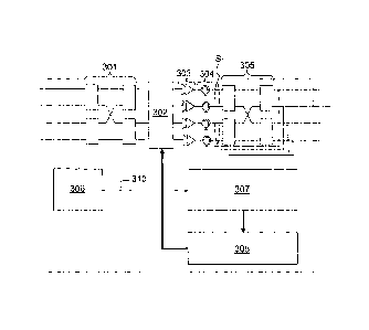
Figure 3 shows diagrammatically a schematic of a self-compensated
multi-port amplifier according to the invention. This amplifier is composed of
an input matrix 301 comprising 4 input pathways and 4 hybrid couplers
connected together so as to represent a Butler matrix. In a more general
case, the input matrix 301 comprises N input and output pathways and
(N/2)*M hybrid couplers, with N = 2m.
The outputs of the input matrix 301 are connected to a phase and amplitude
compensation device 302 composed of attenuators and of phase shifters and
which is inserted upstream of a chain 303 of tube amplifiers the function of
which is to amplify the signal of each pathway. Each tube amplifier is
connected to a power isolator 304 which makes it possible notably to protect
WO 2011/051146 CA 02778855 2012-04-24
PCT/EP2010/065775
=
the tube amplifiers 303. Each power isolator 304 is thereafter connected to
one of the inputs of an output matrix 305 whose transfer function is identical
to that of the previous input matrix 301. This output matrix 305 is also
composed of hybrid couplers and produces as output N amplified signals.
5 Upstream of the system, a signal generator 306 produces a reference
signal,
for example a signal with pure carrier frequency, which is transmitted on the
first input port of the device. The signals delivered on the N output pathways
are thereafter extracted by a measurement device 307 which separates the
reference signal from the communication signals and performs an estimation
10 of the amplitude error and phase error in the reference signal, doing so
for
each of the output pathways. These amplitude error and phase error
measurements are stored in a memory in matrix form and then a signal
processing device 308 utilizes these measurements with the aim of
producing a correction in phase and amplitude which is applied retroactively
by the compensation device. The measurement device is previously
calibrated so as to actually produce a zero phase error and zero amplitude
error when the signal extracted at output is identical to the reference signal
generated at input.
In a variant embodiment for which the multi-port amplifier according to
the invention is embedded onboard a satellite in orbit, the signal processing
device 308 may be implemented in a ground facility. In this case, the
amplitude and phase error measurements extracted are transmitted to the
ground by way of a telemetry downlink, and the corrections generated by the
signal processing device are thereafter transmitted aboard the satellite by
way of a remote control uplink.
In the case where the reference signal injected at the input of the
system is a sinusoidal signal whose frequency spectrum is a pure frequency
such as illustrated in Figure 2, the function of the measurement device 307 is
the detection of amplitude and of phase of this reference signal which is
transmitted simultaneously with the communication signal. A possible
WO 2011/051146 CA 02778855 2012-04-24
PCT/EP2010/065775
11
solution for carrying out this amplitude and phase detection consists in
implementing a coherent demodulation of the composite signal such as
shown diagrammatically with the support of Figure 3a.
A vector 30 comprising the measurements of signal delivered on the N
output pathways of the amplifier according to the invention is provided as
input to the measurement device 307. For each component of the vector 30,
a bandpass filtering 31 is applied so as to extract the reference signal from
the useful signal. The filtered signal is thereafter correlated 32,33 with the
reference signal 34 and the reference signal phase-shifted by 900 35. The
two correlated signals obtained are filtered by means of a low-pass filter
36,37 and then an analog digital conversion 38,39 is applied so as to provide
the in-phase pathway I and quadrature pathway Q to a calculation module 40
which determines the errors in the amplitude A = + Q2 and in
the phase
cDo = arg(*) for each of the output pathways of the amplifier. The amplitude
error and phase error measurements 41 are thereafter delivered to the signal
processing device 308.
Other implementations of the measurement device 307 are possible
knowing that its technical function consists in extracting the reference
signal
from the useful signal and then estimating the amplitude and the phase which
have impacted the reference signal after it has passed through the various
component stages of the amplification device according to the invention.
In a variant embodiment of the invention, the reference signal 310 is
spread spectrally with the aid of a spreading code. In this case, the
measurement device 307 includes in addition to the elements previously
described a module 42 for despreading the signal received on the basis of
the spreading code used which is provided by the generator 306. A
schematic of a possible implementation of such a device 307 is represented
in Figure 3b. The despreading of the signal can be done by a scheme known
to the person skilled in the art with the aim of extracting the reference
signal
WO 2011/051146 CA 02778855 2012-04-24
PCT/EP2010/065775
12
from the useful signal, so as thereafter to estimate its amplitude and its
phase. The benefit in using a spread-spectrum signal resides in the fact that
such a signal is more discrete and exhibits an energy which is spread
throughout the frequency band used.
One of the essential characteristics of the present invention resides in
the determination of the corrections 302 in phase and amplitude which are
determined by the signal processing device 308 on the basis of the amplitude
and phase measurements obtained, for each output pathway, by the
measurement device 307.
The constituent elements of the amplifier system according to the
invention may be modeled on the basis of the following quantities.
The input matrix 301 is defined by its matrix response denoted MI31. In
the most general case, the matrix MB1 possesses N rows and N columns
where N is the number of input ports of the system. The integer N is
preferably equal to a power of 2, N = 2P with p a positive integer strictly
greater than 0. This matrix is obtained, for example, by measurement.
In a similar manner, the output matrix 305 is defined by its matrix response
MB2 which also possesses N rows and N columns.
The phase/amplitude compensation device 302 is modeled by the diagonal
7 ale' 0 0 0
0 a2 e2 0 0
matrix DA_, 0 0 a3e 0 , in the
case where N= 4, with
l)3
0 0 0 a4e 14'4 )
ai the amplitude compensation and cl); the phase compensation applied to
each pathway by the device 302 upstream of the chain of amplifiers 303, i
varying from 1 to N.
WO 2011/051146 CA 02778855 2012-04-24
PCT/EP2010/065775
13
In a similar manner, the influence of the amplifiers 303 may be modeled with
(G, 0 0 0"
0 G2 0 0
the aid of the matrix D Ampli
0 0 G3 0 in the case where N =4,
0 0 0 G4/
with Gi the gain of each amplifier for i varying from 1 to N.
In the subsequent description, reference will be made to the various
signals taken at distinct points of the device with the aid of the following
notation. Each variable is a vector with N components which each
correspond to the signal on one of the N pathways of the device.
( e\
0
E = denotes the
reference signal injected on input port number 1
0
0
of the device.
E,=MBI.E denotes the signal obtained at the output of the input
matrix 301.
E2 = DA_0.MBI.E denotes the signal obtained at the output of the
phase/amplitude compensation device 302.
Si= DAniph.E2 denotes the signal obtained at the output of the chain of
amplifiers 303 after extraction of the reference signal and of the useful
signal
by the measurement device 307.
Finally, S = MB2.51 denotes the signal obtained at the output of the
output matrix 305.
The measurement device 307 delivers at its output a measurement of
the amplitude and of the phase of the reference signal on each output
pathway. These measurements make it possible to create the vector S.
WO 2011/051146 CA 02778855 2012-04-24
PCT/EP2010/065775
14
On the basis of the previous relations, the following relation is
deduced:
= Di/mph DA_,I,MBiE (1)
With S1 =
And from this is deduced the following relation which connects the vector Si
to the other variables of the system.
( (
52 S
e.G2= a2 e 1(1)2 . nu- 2 ,1
1 = = (2)
S3 e.G3'a3e 14)3 .MB1 3'1
e.G4= a4 ell'4.M
B 14,1
Where MB:'',MB2'1,MB3',MB" are the components of the first row of the
matrix M61.
Finally, relation (3) is arrived at, which makes it possible to determine, for
any
i varying from 1 to N (N= 4 in our example), the complex gains of each
amplifier:
1
1
G, = S e.M i (3)
=aie
The vector Si is calculated on the basis of the vector S obtained by
measurements and of the output matrix MB2.
The reference signal e is known to the user, as is the input matrix MBi.
The values of the amplitude setpoint and phase setpoint (matrix Diva)) are
initialized at the start of the method to given initial values, a(); and
The method according to the invention thereafter consists in determining at
various instants of temporal sampling new values a'i and ctoi of
amplitude/phase setpoint so as to correct the system isolation defects.
One of the objectives of the self-compensation in phase and amplitude
of the system according to the invention is to correct the imperfections of
the
amplifier chain modeled by the matrix DAmpii. In order that the system be as
close as possible to theory and that the isolation between each output
CA 02778855 2012-04-24
WO 2011/051146
PCT/EP2010/065775
pathway be as optimal as possible, it is necessary for each of the amplifiers
303 used on each of the pathways of the system to exhibit the same
response in terms of amplitude and phase. This condition is equivalent to a
modeling of the system which satisfies the following relation:
5
DA, .D Amph = G d (4)
Where G is a complex gain and Id the identity matrix.
Relation (4) translates the compensation by the device 302 modeled by the
10 matrix
DA_d, of the imperfections of the chain of amplifiers 303 modeled by the
matrix DAmpii in such a way as to obtain an identical complex gain on each
pathway; one speaks of iso-length of the N paths making up the device.
To obtain this result, a reference pathway should initially be chosen from
among the N possible pathways. By default the pathway of index 1 is taken
15 as reference pathway, the gain Gi of the amplifiers of the other N-1
pathways
should then be compensated by the difference in gain G1 between each
pathway of index i and the reference pathway.
The reference pathway may be taken equal to any pathway. The
compensation of the gains of the amplifiers can also be performed with
respect to a virtual reference whose gain corresponds to the average of the
gains of all the pathways, to the minimum or to the maximum of the gains
over the whole set of pathways.
Therefore, the following quantities are calculated, for i varying from 2 to N:
AZ1,, = (a,+ G1)¨(a1 +1G11) (5)
where all the terms of the relation are expressed in decibels, and I I denotes
the modulus of a complex number, and
A031)1,, = (0, + arg(G, ))¨ (01 + arg(G, )) (6),
where all the terms of the relation are expressed in degrees and arg()
denotes the argument of a complex number.
WO 2011/051146 CA 02778855 2012-04-24
PCT/EP2010/065775
16
The amplitude/phase self-compensation of the system must culminate in a
complex gain, that is to say an amplitude and a phase, that is identical on
each pathway at the output of the chain of amplifiers 303.
Accordingly, the non-linearity of said amplifiers needs to be taken into
account. Indeed, the amplitude, respectively the phase, at the output of an
amplifier is not necessarily proportional to the amplitude, respectively the
phase, at the input of the same amplifier. In practice an amplifier i exhibits
a
first transfer function fi AM,Am which connects the amplitude of the input
signal
to the amplitude of the output signal, and a second transfer function fl AM,PM
which connects the phase of the input signal to the amplitude of the output
signal. An example of such transfer functions is illustrated with the support
of
Figures 4a and 4b. The curve 404 represents the variation of the power of
the output signal 402 as a function of that of the input signal 401. The
region
L of the curve 404 is linear while the remainder of the curve is not. Likewise
the curve 405 represents the variation of the phase of the output signal 403
as a function of the power of the input signal 401.
The amplitude IBQ of the signal at the input of the amplifier of the
pathway of index i, which is connected to the amplitude OBO; of the signal at
the output of the same amplifier, is then introduced through the following
relation:
IBO, = fAi A,,,AA4(0B0,) (7)
and the phase of the signal at the input of the same amplifier is given by the
relation: 0, = fAmi ),A,f (0B01) = arg( G, ) (8)
The value of the signal at the output of the amplifier is obtained on the
basis
of the component i of the vector S1 introduced previously.
It is then sought to compensate the amplitude of the output signal of each
amplifier by the quantity ______________________________________ obtained in
relation (5) so as to obtain a new
value OBdi = OBOi- A7
41,i of the amplitude of the output signal.
WO 2011/051146 CA 02778855 2012-04-24
PCT/EP2010/065775
17
The new amplitudes and phase of the input signal of the amplifier are
thereafter calculated with the aid of the following relations:
IBO' , = f A' m ,Am (0B01,)
(9)
fAim J,A4 (OBO' ,)
Finally the last calculation step makes it possible to obtain the new values
of
amplitude and phase setpoint that the calculation device 308 provides to the
compensation device 302 at a later instant:
a',= a, + IBO' IBO,
(10)
¨ (OHO)
In a variant embodiment of the invention, the tube amplifiers 303 may
be replaced with solid-state power amplifiers, known by the abbreviation
SSPA.
Another variant embodiment of the invention is now described for
which the knowledge of the input matrix MB,, output matrix MB2 and the
matrix DAmpii modeling the influence of the amplifiers 303 is not necessary.
Referring to relations (1), (2) and (3) introduced hereinabove, it is
noted that the self-compensated system according to the invention requires
the knowledge of the matrices MB, and MB2 as well as the calculation
(according to relation (3)) of the matrix DAmpli. This a priori knowledge
involves a measurement, by external means, of the responses of the input
Butler matrix and output Butler matrix so as to model their real influence
which may differ from the theoretical Butler matrices on account of their
production-related imperfections.
The real matrix response MB, of the input Butler matrix may be
decomposed as the product of two terms MB, = mierror. mBith, where MBith is
the theoretical input Butler matrix and Mier is the diagonal matrix
comprising the errors or differences between the theoretical matrix and the
CA 02778855 2012-04-24
WO 2011/051146
PCT/EP2010/065775
18
real matrix. In the same manner, it is possible to write for the output matrix
of
the system MB2 = mB2th. werror
By taking into account the imperfections of the Butler matrices and
through analogous reasoning to that described previously with the support of
relation (4), this time it is sought to render the N paths passing through the
power amplifiers between each theoretical Butler matrix iso-length. This
condition is equivalent to a modeling of the system which satisfies the
following relation, with G a complex gain and Id the identity matrix:
m 2 error D Amplim / error = G.I d (11)
The amplitude setpoint ai and phase setpoint crii determined by the
calculation device 308 and transmitted to the compensation device 302 are
thereafter determined in an analogous manner to the reasoning described
previously with the support of relations (3) and (5) to (10) with the
exception
that the corrective terms aiej`Di making up the diagonal matrix Divo also
integrate the imperfections related to the diagonal error matrices Mie"r and
M2e"r. The relations making it possible to determine the complex gains Gi of
each amplifier, in particular relation (3) and the relation connecting the
intermediate vector S1 and the output vector S, are used with the theoretical
matrices MBith and MB2th rather than the real ones.
In another aspect of the invention, the characteristics f,4,111 and
fAl,,,,,pm of the amplifiers of each pathway need no longer be taken into
account. The amplitude compensation a'i is determined directly on the basis
of the output amplitude value OB01; of each amplifier through the relation:
a' ,= a, + q(OBO' ,-0B0,) (12)
with 1 a multiplicative coefficient less than 1 in absolute value.
WO 2011/051146 CA 02778855 2012-04-24
PCT/EP2010/065775
19
This simplification makes it possible to circumvent the knowledge of the
precise characteristic f' of each
amplifier while ensuring convergence
of the calculations to a finite limit value in a reasonable time.
Moreover the phase compensation c13'; may be determined through the
following relation:
= (1), ¨ A(13 (13)
The phase correction determined according to relation (13) is intrinsically
composed of two terms: a phase rotation introduced by the tube amplifier and
dependent on its output power 0B01 and a phase discrepancy due to the
characteristics of the elements constituting each pathway of the MPA system.
During the first iteration of the calculation, the second term is compensated
and only the first term evolves as the iterations proceed. The total phase
control, namely the sum of the successive corrections applied at each
iteration, then tends to an increasingly stable value as the amplitude
compensation converges. The phase compensation determined according to
relation (13) taking no account of the phase response of each tube amplifier,
this compensation is imperfect but nevertheless allows convergence to a limit
value in a reasonable time.
Figure 5 illustrates the performance of the self-compensated system
and the gain obtained as regards the isolation of the output pathways. The
left part of the figure represents the reference signal SREF, here a pure-
carrier
signal, inserted between two communication signals C1 and C2. In this figure
is represented the isolation I obtained between the amplified signal on the
main pathway and the residual present on the secondary pathways. The
isolation 11 is of the order of 13 dB. The same composite signal is
represented in the right part of the figure but in the case where the system
has been self-compensated by the previously described method according to
the invention. The isolation 12 obtained is improved and this time is of the
order of 33 dB.
CA 02778855 2012-04-24
WO 2011/051146
PCT/EP2010/065775
In another variant embodiment of the invention, the phase and
amplitude compensation is updated as soon as the isolation I measured on
the reference signal is greater than a given threshold. One then speaks of
5 adaptive structure to denote the principle which consists in adapting the
compensations in terms of phase and amplitude in the course of time as a
function of a given criterion. Adaptive compensation is notably necessary
when the errors which impact the system evolves in the course of time as a
function of the operating conditions. On the other hand, one speaks of static
10 compensation when the latter is performed just once to correct a static
error
which does not evolve in the course of time.
The self-compensated multi-port amplification system according to the
invention presents notably the main advantage of ensuring self-
15 compensation in terms of phase and amplitude of the system in the
presence
of traffic, that is to say without interrupting transmission. It is
particularly
adapted to satellite transmission systems. In the assembly, integration and
test (AIT) phase the invention affords an aid in the search for the optimal
settings of the system so as to maximize performance. In the in-orbit test or
20 utilization (I0T) phase the device is self-compensated automatically by way
of the compensation loop which can act from a ground facility to an onboard
facility or be situated entirely on board.
The main objective of the multi-distributed amplification system
according to the invention is the self-compensation in terms of amplitude and
phase of the intrinsic defects of the hardware components which constitute
each amplification pathway so as to ensure maximum inter-pathway isolation.
Another application of the system according to the invention relates to
the detection and location of a fault affecting a power amplification chain on
one of the pathways of the system. Indeed, as explained previously, the
invention makes it possible notably to determine the vector S1 composed of
the powers of the output signals of each chain of amplifiers 303 on each
CA 02778855 2012-04-24
WO 2011/051146
PCT/EP2010/065775
21
pathway. On the basis of this information, a detection threshold may be
applied to each power of the vector S1 so as to determine whether the
estimated output power is abnormally low, which would result from an
amplifier operating defect. The detection threshold is determined as a
function of the power of the signal emitted and of the operating point aimed
at
by the application.
When a fault is located on one of the pathways of the amplification
system according to the invention, a chain of amplifiers 303 may be replaced
with a redundant chain provided for this purpose. A switching of the inputs
.. and outputs of the defective chain of amplifiers to the redundant chain is
then
performed and a new isolation calculation according to the invention is
carried out.