Note: Descriptions are shown in the official language in which they were submitted.
CA 02779062 2012-04-26
1 606831W001
DESCRIPTION
TITLE OF THE INVENTION: SEMICONDUCTOR LASER MODULE
TECHNICAL FIELD
[0001] The
present invention relates to a semiconductor
laser module in which a semiconductor laser element
which emits light by the supply of a current is
hermetically sealed.
BACKGROUND ART
[0002] In
semiconductor lasers for use in a machining
field or the like, an increase in output has been
strongly required. There are many examples in which
the increase in output is generally achieved by
stacking an array in which a large number of
semiconductor lasers are arranged in one element or
by broadening which broadens a light emitting area.
In the semiconductor lasers of such a structure,
respective laser elements are generally arranged
electrically parallel; and therefore, a current
which flows through the laser element becomes large
as the increase in output is progressed and, in
recent years, there is also an example in which a
current value is approximately several tens of
amperes.
[0003] When the semiconductor laser module is aired out,
deterioration of an element end surface or
deterioration of a wire bonding portion is advanced
due to moisture or the like; and therefore, the
semiconductor laser module is often contained in an
hermetic package.
Such a package includes: a
component generally referred to as a "stem" which is
composed of a base portion and a lead pin; and a cap
provided with a window from which laser light is
taken out. There are many cases where the lead pin
CA 02779062 2012-04-26
2 606831W001
is joined and fixed to the base portion by an
insulation seal material such as glass and the cap
is joined and fixed to the base portion by electric
resistance welding.
[0004] The cap and the
base portion of the stem are
generally made of carbon steel or iron-nickel alloy
in consideration of welding quality.
Furthermore,
with regard to the material of the lead pin, in a
cooling process from a temperature of approximately
1000 C at which the glass is melted till returning
to ordinary temperature during sealing process with
glass or in the case where a temperature change is
generated during using, in order to prevent a glass
portion from breaking down due to a difference in
the coefficient of linear expansion, the base
portion and the lead pin need to use material which
is close to the glass member in the coefficient of
linear expansion as much as possible. Therefore, in
the case where the iron-nickel alloy is used as the
material of the lead pin, an iron-nickel alloy in
which the nickel content is approximately 50% by
mass that is close to the base portion in the
coefficient of linear expansion is used.
[0005] Furthermore,
in the case where a large current is
supplied to the semiconductor laser module, magneto-
striction deformation under the influence of a
magnetic field is generated, the magnetic field
being generated by the current flowing through the
lead in when the lead pin is a magnetic material.
More particularly, in the case where an alternating
current or a pulse current is supplied, repeated
deformation due to magneto-striction is generated in
the lead pin; and therefore, there is a case where a
CA 02779062 2012-04-26
3 6068311001
crack is generated due to fatigue at a boundary
surface between the lead pin and the glass material
or at the glass material itself.
Further, in the
case where frequency of the alternating current or
the pulse current is in a zone of audibility of the
person, the repeated deformation of the lead pin
causes a sound source depending on a housing in
which the semiconductor laser module is located and
a locating method; and thus, a problem exists in
that the sound source is amplified by the
surrounding housing or the like to generate noises.
[0006] In order to solve the aforementioned problem, it is
conceivable that a non-magnetic material is used for
the lead pin. In
Patent Document 1, copper,
aluminum, titanium, austenitic stainless steel, and
their alloys are disclosed as the lead pin material.
In Patent Document 2, a nickel-molybdenum alloy
(hastelloy) or nickel-chromium-molybdenum alloy is
disclosed as the lead pin material.
RELATED ART DOCUMENT
PATENT DOCUMENT
[0007] Patent Document 1: Japanese Unexamined Patent
Publication No. 2003-216887
Patent Document 2: Japanese Unexamined Patent
Publication No. 2005-353291
DISCLOSURE OF THE INVENTION
PROBLEMS TO BE SOLVED BY THE INVENTION
[0008] However, the coefficients of linear expansion of
the materials :of. the copper, aluminum, and
austenitic stainless steel disclosed in Patent
Document 1 are as follows: 19x10-6 [/K] of copper,
23x10-6 [7K] of aluminum, 8.4x10⁻⁶ [1K] of titanium,
and 16.4x10⁻⁶ [/K] of austenitic stainless steel,
CA 02779062 2012-04-26
4 606831W001
respectively.
All the coefficients except for
titanium have a large difference with respect to the
coefficient of linear expansion 9.5x10⁻⁶ [/K] of
borosilicate glass and soda-lime glasses, both of
which being used as a sealing glass; and accordingly,
a problem exists in that there is a case where a
crack is generated at the boundary portion between
the lead pin and the glass material or at the glass
material due to a difference in the amount of heat
shrinkage in the cooling process during sealing with
glass and thus hermetic seal cannot be sufficiently
kept.
Titanium is difficult to be refined and
processed and is expensive.
[0009] Volume resistivities of the titanium and austenitic
stainless steel disclosed in Patent Document 1 and
volume resistivities of the nickel-molybdenum alloys
and nickel-chromium-molybdenum alloys disclosed in
Patent Document 2 are as follows: 53 [g Q cm] of
titanium, 74 [
cm] of austenitic stainless steel,
and 110 [ g .cm] of nickel-
molybdenum alloys and
nickel-chromium-molybdenum alloys, respectively.
The volume resistivities are equal to or more than
10 times as compared to 1.7 [g Q =cm] of copper which
is generally used for large current wiring; and
accordingly, a problem exists in that there is a
case where hermetic seal cannot be sufficiently kept,
for example, when a large current flows, a wiring
material is elongated or contracted due to
temperature rise by the Joule heat at the wiring
portion and a crack is generated between the lead
pin and the glass material.
[0010] In
order to avoid the problem caused by the heat
CA 02779062 2012-04-26
606831W001
generation of the lead pin described above, a method
of reducing wire resistance of the lead pin by
enlarging the diameter of the lead pin through which
the current flows, is also conceivable. However,
5 when the diameter of the lead pin is equal to or
more than approximately 1 romp, it becomes difficult
to ensure hermetic seal itself; and therefore, the
large current needs to be flown through the lead pin
having the diameter of approximately 1 mmp at a
maximum.
[0011] The present invention has been made to solve the
foregoing problem, and an object of the present
invention is to provide a semiconductor laser module
using hermetic terminals in which breakage is not
made in a cooling process during sealing with glass,
magneto-striction deformation is in an acceptable
range, and a large current can be flown.
MEANS FOR SOLVING THE PROBLEMS
[0012] According to the present invention, there is
provided a semiconductor laser module which includes
a semiconductor laser element which emits light by
the supply of a current; a package base having a
through hole; a lead pin which passes through the
through hole and supplies the current to the
semiconductor laser element; a glass material which
seals the through hole through which the lead pin
passes through; and a cap which has a window from
which light emitted by the semiconductor laser
element is taken out and has the semiconductor laser
element in the inside thereof, the cap being
hermetically joined to the package base. In
the
semiconductor laser module, the lead pin is an iron-
nickel alloys in which the coefficient of linear
CA 02779062 2014-08-13
6
expansion is not higher than a predetermined ratio
in difference with the glass material, the
saturation magneto-striction constant is not higher
than a predetermined value, and volume resistivity
is not hlgher than a predetermined rate.
According to an aspect of the present invention,
there is provided a semiconductor laser module
comprising:
a semiconductor laser element which emits light by
the supply of a current;
a package base having a through hole;
a lead pin which passes through the through hole
and supplies the current to said semiconductor laser
element;
a glass material which seals the through hole
through which said lead pin passes through; and
a cap which has a window from which light emitted
by said semiconductor laser element is taken out and
has said semiconductor laser element in the inside
thereof, said cap being hermetically joined to said
package base,
wherein said lead pin is an iron-nickel alloys in
which the coefficient of linear expansion is not
higher than a predetermined ratio in difference with
said glass material, the saturation magneto-
striction constant is not higher than a
predetermined value, and volume resistivity is not
higher than a predetermined rate, and
wherein said lead pin has the nickel content which
is equal to or higher than 70% by mass and equal to
or lower than 85% by mass.
CA 02779062 2014-08-13
6a
ADVANTAGEOUS EFFECT OF THE INVENTION
[0013] A
semiconductor laser module according to the
present invention includes a semiconductor
laser
element which emits light by the supply of a
current; a package base
having a through hole; a
lead pin which passes through the through hole and
supplies the current to the semiconductor laser
element; a
glass material which seals the
through hole through which the lead pin passes
through; and a cap which has a window from which
light emitted by the semiconductor laser element is
taken out and has the semiconductor laser element in
the inside thereof, the cap being hermetically
joined to the package base.
In the semiconductor
laser module, the lead pin is an iron-nickel alloys
in which the coefficient of linear expansion is not
higher than a predetermined ratio in difference with
the glass material, the saturation magneto-striction
constant is not higher than a predetermined value,
and volume resistivity is not higher than a
predetermined rate, whereby, breakage is not made in
a cooling process during sealing with glass,
magneto-striction deformation is in an acceptable
range, and a large current can be flown.
BRIEF DESCRIPTION OF THE DRAWINGS
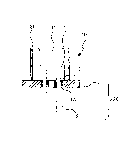
[0014] Fig. 1 is a sectional view showing the
configuration of a semiconductor laser module
according to Embodiment 1 of the present invention;
CA 02779062 2012-04-26
7 606831W001
Fig. 2 is a graph showing the relationship between
the nickel content of iron-nickel alloy and the
saturation magneto-striction constant;
Fig. 3 is a graph showing the relationship between
the nickel content of iron-nickel alloy and the
coefficient of linear expansion;
Fig. 4 is a graph showing the relationship between
the nickel content of iron-nickel alloy and volume
resistivity;
Fig. 5 is a graph showing the relationship between
the nickel content of iron-nickel alloy and thermal
conductivity; and
Fig. 6 is a view for explaining material
characteristics of materials available for a lead
pin and other materials.
MODE FOR CARRYING OUT THE INVENTION
[0015] A semiconductor laser module of the present
embodiment of the present invention will be
described with reference to drawings.
[0016] Embodiment 1.
Fig. 1 is a sectional view showing the
configuration of a semiconductor laser module 100 in
the present embodiment. In
Fig. 1, in the
semiconductor laser module 100, a cap 30 is provided
with a glass window 31 from which light emitted by a
semiconductor laser element 10 is taken out and the
cap 30 is hermetically joined to a package base 1 to
which the semiconductor laser element 10 which emits
the light by the supply of a current is fixed.
[0017] A predetermined number of circular through holes lA
are formed in the package base 1, one lead pin 2
passes through each of the through holes lA and a
glass material 3 is embedded in the through hole 1A
CA 02779062 2012-04-26
8 606831W001
around the lead pin 2. The package base 1 where the
lead pins 2 are passed through and fixed, is an
hermetic terminal 20 referred to as a "stem."
[0018] A
carbon steel or an iron-nickel alloys in which
the nickel content is approximately 50% by mass is
used as a material of the package base 1 and the cap
30; and a soda-lime glasses is used as the glass
material 3. Furthermore, a material of the lead pin
2 is an iron-nickel alloys in which the nickel
content is approximately 78.5% by mass (78 permalloy
or permalloy A) which is particularly near zero in
saturation magneto-striction constant and the
maximum in initial magnetic permeability, among
iron-nickel alloys in which the nickel content is 70
to 85% by mass (PC permalloy) regulated by standard
"JIS C 2531, 1999: Iron nickel soft magnetic
materials."
[0019] The coefficient of linear expansion of the soda-
lime glasses serving as the material of the glass
material 3 is 9.5x10⁻⁶ [/K]; however, the coefficient
of linear expansion of the carbon steel or the iron-
nickel alloys in which the nickel content is
approximately 50% by mass, serving as the material
of the package base 1 also has a value of 11.1x10⁻⁶
[/K] which is near to that of the soda-lime glasses.
Furthermore, the coefficient of linear expansion of
the permalloy A serving as the material of the lead
pin 2 also has a value of approximately 12x10-6 [/K]
which is near to that of the soda-lime glasses.
[0020] Now, a method of manufacturing the hermetic
terminal 20 for use in the semiconductor laser
module 100 in the present embodiment will be briefly
described. First, the through hole lA is formed at
CA 02779062 2012-04-26
9 606831W001
a predetermined position of the package base 1.
Subsequently, the lead pin 2 is located at the
center of the through hole 1A. The
melted glass
material 3 is poured into the through hole 1A around
the lead pin 2 to seal the through hole 1A. The
glass material 3 is solidified and the hermetic
terminal 20 is completed at ordinary temperature.
The semiconductor laser element 10 is fixed at the
predetermined position of the package base 1 with
adhesive or the like; and the lead pin 2 and the
semiconductor laser element 10 are connected by
wiring therebetween.
After that, covering is made
by the cap 30; dry air or the like is filled; and
the package base 1 and the cap 30 are joined by
electric resistance welding. Thus, the
semiconductor laser module 100 is completed.
[0021] As described above, in the case of melting the
glass material 3 during manufacturing of the
hermetic terminal 20, the temperature reaches a high
temperature of approximately 1000 C in order to melt
the glass material 3; and therefore, the nearer the
coefficients of linear expansion of the package base
1, the glass material 3, and the lead pin 2 are, the
smaller the stress at ordinary temperature becomes.
The semiconductor laser module 100 of the present
embodiment is composed of the package base 1, the
glass material 3, and the lead pin 2, those of which
are small in difference between the coefficients of
linear expanSion. Therefore, stress generated in a
sealing process with glass is small; and thus, a
crack is difficult to generate between the glass
material 3 and the lead pin 2 and between the glass
material 3 and the package base 1.
CA 02779062 2012-04-26
606831W001
[0022] Next, the case where the semiconductor laser module
100 is driven by applying an alternating current or
a pulse current to the lead pin 2 will be described.
When the current flows through the lead pin 2, a
5
magnetic field is generated in the inside of the
lead pin 2 by the current. Deformation is generated
in the lead pin 2 in response to the saturation
magneto-striction constant inherent to the material
under the influence of the magnetic field. The
10
material of the lead pin 2 in the present embodiment
is the permalloy A which is small in saturation
magneto-striction constant; and therefore, magneto-
striction deformation is hardly generated. As
a
result, fatigue fracture of a glass seal portion due
to deformation and the generation of noise are not
generated.
[0023]
Furthermore, the lead pin 2 in the present
embodiment is the permalloy A; and therefore, volume
resistivity can be reduced to 15 [g Q.cm] that is
approximately 42% as compared to the iron-nickel
alloy in which the nickel content is approximately
50% by mass that has been generally used in the past.
Therefore, even when a large current flows through
the lead pin 2, the amount of heat generation of the
lead pin 2 can be reduced and thus the amount of
expansion and contraction due to the heat generation
of the lead pin 2 can be reduced. As a result, an
hermetic package with high reliability can be
obtained without generating fatigue fracture of the
glass seal -portion during driving of the laser
module.
According to the present embodiment, for example,
even when a large average current of 5A continuously
CA 02779062 2012-04-26
11 606831W001
flows through the lead pin 2 having 1 mm9, a high
reliability semiconductor laser module in which
hermetic seal is hardly broken due to the generation
of a crack can be obtained.
[0024] The reason why the permalloy A is adopted for the
material of the lead pin 2.
Fig. 2 is a graph
showing the relationship between the nickel content
in the iron-nickel alloy and the saturation magneto-
striction constant.
Fig. 3 is a graph showing the
relationship between the nickel content in the iron-
nickel alloy and the coefficient of linear expansion.
Fig. 4 is a graph showing the relationship between
the nickel content in the iron-nickel alloy and
volume resistivity.
Fig. 5 is a graph showing the
relationship between the nickel content in the iron-
nickel alloy and thermal conductivity. Fig. 6 is a
view for explaining material characteristics of
materials available for the lead pin and other
materials.
[0025] The coefficient of linear expansion of the
permalloy A is 12x10-6 [/K] and is different with
respect to 10.8x10⁻⁶ [/K] of iron and 9.5x10⁻⁶ [1K]
of soda-lime glass, each material being served as
the material of the package base 1; and the
differences are an increase of 11.1% and an increase
of 26.3%, respectively, each increase being in an
acceptable range. Therefore, when the melted glass
material is solidified, stress of the glass material
generated due to the differenoe between the
coefficients of linear expansion can be lowered to a
level at which a crack or the like is not generated.
The saturation magneto-striction constant of the
permalloy A is approximately 5x10⁻⁶ and is
CA 02779062 2012-04-26
12 606831W001
approximately 1/4 with respect to approximately
20x10-6 of the case where the nickel content is 50%
by mass (Fe-50 wt% Ni alloy). Volume resistivity of
the permalloy A is 15 [g Q.cm] and is approximately
42% with respect to approximately 35 [12, Q=cm] of the
case of the Fe-50 wt% Ni alloy.
Thermal
conductivity of the permalloy A is 33.5 [W/m.K] and
is approximately 2.39 times with respect to 14
[W/m.K] of the case of the Fe-50 wt% Ni alloy.
[0026] As is apparent from Fig. 2 to Fig. 6, an iron-
nickel alloy in which the saturation magneto-
striction constant is near zero, the coefficient of
linear expansion is a value near to that of the
glass material, and the volume resistivity is small
as much as possible, is the case where the nickel
content is approximately 80% by mass. The
reason
why the permalloy A in which the nickel content is
78.5% by mass is adopted for the material of the
lead pin 2 is that the permalloy A is excellent in
machine workability such as rolling and cutting,
easy to obtain materials and to form in a pin shape,
and capable of producing inexpensively.
[0027] Even if the permalloy A is not available, as far as
an iron-nickel alloy is one regulated by standards
such as the Japanese Industrial Standard (JIS) and
the International Electrotechnical Commission (IEC),
such iron-nickel alloys is easier to obtain than a
substandard alloy. In
the case of JIS, an iron-
nickel alloys in which the nickel content is 70 to
85% by mass (PC permalloy) regulated in "JIS C 2531,
1999: Iron nickel soft magnetic materials" is
preferable. In
the case of the TEC, an iron-nickel
CA 02779062 2012-04-26
13 606831W001
alloys in which the nickel content is 72 to 83% by
mass, regulated as a type of Ell in "IEC 60404-8-6,
1999: Soft metal magnetic materials" is preferable.
[0028]
As the material of the lead pin, an iron-nickel
alloys in which the coefficient of linear expansion
is not _higher than a predetermined ratio in
difference with the sealing glass material, the
saturation magneto-striction constant is not higher
than a predetermined value, and the volume
resistivity is not higher than a predetermined rate,
is preferable.
Larger thermal Conductivity is
preferable so as to transfer Joule heat at the lead
pin and heat generation due to light emission at the
semiconductor laser element to the outside of the
package. In the iron-
nickel alloys, in order to
have an optional function, a material to which
elements such as molybdenum, chromium, copper, and
niobium are added to the iron-nickel material up to
approximately 10% by mass, may be used.
[0029]
Furthermore, an iron-nickel alloy in which the
nickel content is near 30 9/D by mass is also
substantially zero in the saturation magneto-
striction constant; and therefore, a similar effect
can be obtained. However, volume resistivity is 75
[g Q =cm]; and therefore, such iron-nickel alloys is
not suitable for other than the case where the
diameter of the lead pin can be -increased or the
length of the lead pin can be shortened in the case
-
of applying a large current.
DESCRIPTION OF REFERENCE NUMERALS
[0030] 100 Semiconductor laser module
10 Semiconductor laser element
CA 02779062 2012-04-26
14 606831W001
1 Package base
1A Through hole
2 Lead pin
3 Glass material
20 Hermetic terminal
30 Cap
31 Glass window