Note: Descriptions are shown in the official language in which they were submitted.
CA 02779356 2012-04-30
WO 2011/054614 PCT/EP2010/064862
1
A Nanohole Array Biosensor
This invention relates to a nanohole array biosensor, and a
biosensing apparatus including such a sensor.
Background
W.L. Barnes, A.Dereux, T.W. Ebbesen, Nature 24 (2003)
824-830 discloses extraordinary optical transmission (EOT)
through sub-wavelength apertures where visible light,
normally incident on a metal film containing a periodic
array of sub-wavelength nanoholes, exhibits a peak
transmission intensity which is orders of magnitude higher
than had been predicted previously. The nanohole arrays
were fabricated in an optically thick gold film deposited
on a glass substrate using a focused ion beam milling.
A short ordered array of nanoholes acts in a similar way to
a periodic grating allowing the incident radiation to
stimulate surface plasmon modes of a characteristic
frequency that depends on the dielectric function of the
metal, the periodicity of the hole array and the dielectric
function of medium at the surface of the metal film. The
process by which light transfers through the hole depends
on the thickness of the metal film.
For optically thick films, where the thickness is too great
to allow plasmon/plasmon coupling between the two sides of
the film, the process involves evanescent waves tunnelling
down through the aperture walls resulting in a small
amplitude of light at the emission side, for example, as
disclosed by A. Kishnihan, T. Thio, TJ. Kima, H.J. Lezec,
CA 02779356 2012-04-30
WO 2011/054614 PCT/EP2010/064862
2
T.W. Ebbesen, P.A. Wolff, J. Pendry, L.Martin Moreno, F.J.
Garcia-Vidal, Opt. Commun 200(2001) 1-7. At this point the
plasmons recouple to the metallic film on the opposite side
and their associated fields interfere resulting in the
propagation of light.
For optically thin metal films where there is considerable
plasmon/plasmon overlap the light emission is greatly
enhanced.
P.R.H. Strark, A.E. Halleck, D.N. Larson, Methods 37 (2005)
37-47 discloses the application of nanohole plasmons in the
area of biosensing. This involves a sensing method for
detecting a refractive index change through the variation
in light intensity transmitted through nanohole structures
fabricated on a gold film. The nanohole structures were
fabricated in an optically thick film using a focused ion
beam to produce an array of holes with a periodicity of 500
nm.
Separately, A. Dahlin, M. Zach, T. Rindzevicius, M. Kall,
D.S. Sutherland, F. Hook J. Am. Chem. Soc. 127(2005)
5043-5048 discloses the suitability of EOT for biosensing.
In their experiments nanoholes were fabricated randomly in
an optically thin film of gold and a biotin/neutravidin
immunoassay concept was demonstrated. In both cases, the
biosensor was based on the transmission of light through a
periodic array of nanoholes fabricated on a standard
microscope glass slide.
J.C. Yang, J. Ji, J. M. Hogle, D.N. Larson Biosensors and
Bioelectronics, 24(2009), 2334-2338 discloses constructing
CA 02779356 2012-04-30
WO 2011/054614 PCT/EP2010/064862
3
up to 25 independent nanohole arrays of different
periodicities within a 60pm x 50pm area on a single
substrate for multiplexed plasmonic sensing.
A.Dhawan, J.F. Muth Materials Science and Engineering: B,
149(3), ( 2008), 237-241 discloses arrays of nanoholes
constructed at the tips of individual single mode and
multimode optical fibres and demonstrated their feasibility
for fibre optic sensing.
Surface plasmons (SP's) are refractive index sensitive
charge density oscillations occurring on metal surfaces.
Conveniently stimulated with light via suitable coupling
mechanisms that increase the momentum of the incident light
to satisfy the plasmon dispersion relation, they have been
successfully deployed in a number of commercial instruments
as a method of investigating chemical and biochemical
interactions. As disclosed in US 6,441,904 and US
2006/0108219, these instruments typically employ prisms,
waveguides or gratings to increase the momentum of light
incident on a continuous metal surface containing a layer
of receptive molecules acting as a dielectric medium. Their
sensitivity to changes in the refractive index around the
interface of the metal and dielectric results in changes
the angular distribution, reflected spectra or reflected
intensity of the light. The measurement of which provides a
label free measurement of ligand-receptor binding for
chemical and biochemical assays.
These methods of plasmon resonance detection do not lend
themselves easily to high throughput screening applications
where multiple individual assays are recorded at the one
CA 02779356 2012-04-30
WO 2011/054614 PCT/EP2010/064862
4
time.
Summary of the Invention
The present invention provides a biosensor including a
light transmissive optical component comprising a plurality
of optical fibres fused side-by-side, the fibres extending
between and terminating at opposite faces of the component
for transmission of light through the component, a metallic
film coated on at least part of one face of the optical
component, and a plurality of nanohole arrays formed in the
metallic film.
Preferably the one face of the optical component is formed
with a plurality of depressions and a respective metallic
film nanohole array is formed in at least some of the
depressions.
The invention further provides a method of making a
biosensor including providing a light transmissive optical
component comprising a plurality of optical fibres fused
side-by-side, the fibres extending between and terminating
at opposite faces of the component for transmission of
light through the component, coating a metallic film on at
least part of one face of the optical component, and a
forming plurality of nanohole arrays in the metallic film.
The invention further provides a biosensing apparatus
comprising a biosensor as specified above, a source of
monochromatic light at a given wavelength for illuminating
the nanohole arrays, and processing means for processing
signals output from the light sensing array, wherein the
CA 02779356 2012-04-30
WO 2011/054614 PCT/EP2010/064862
nanoholes have sub-wavelength dimensions and the metallic
film has at least one hole with a super-wavelength
dimension.
5 Brief Description of the Drawings
Embodiments of the invention will now be described, by way
of example, with reference to the accompanying drawings, in
which:
Figure 1 is a schematic diagram of a conventional
arrangement for measuring EOT.
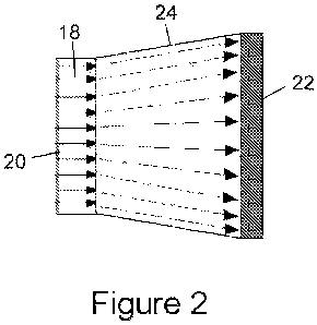
Figure 2 is a schematic side view of an embodiment of a
biosensor according to the invention.
Figure 3 is a schematic diagram of a biosensing apparatus
incorporating a biosensor as seen in Figure 2.
Detailed Description of the Embodiment
Figure 1 shows a prior art nanohole array biosensing
apparatus for measuring EOT. A plurality of sub-wavelength
nanohole arrays is formed in a gold film 10 coated on a
glass slide 12. The gold film 10 is illuminated with
monochromatic light and the light transmitted through the
slide 12 is focussed on a CDD detector (light sensing
array) 14 by an oil immersion lens 16. In use a small
quantity of a biological analyte is placed on each nanohole
array and the intensity of light sensed by the CCD detector
in respect of each nanohole array is analysed in a known
manner to provide information about the sample. A
CA 02779356 2012-04-30
WO 2011/054614 PCT/EP2010/064862
6
disadvantage of this apparatus is that light scattering at
the interface of the nanohole film and the glass slide
reduces the efficiency of light transfer to the CCD
detector.
Figure 2 shows an embodiment of biosensor according to the
invention. The biosensor includes a fibre optic faceplate
18, for example of the type produced by Schott North
America, Inc., Elmsford, NY 10523, USA. The faceplate 18
comprises a plurality of parallel optical fibres fused
side-by-side, the fibres extending perpendicularly between
and terminating at opposite parallel major surfaces of the
faceplate to form an optically transparent plate that
allows the 1:1 transmission of light from one major surface
of the plate to the other. Preferably, each optical fibre
has a core diameter of greater than 6 microns and the fused
faceplate is preferably larger than 1 cm2 in area, most
preferably up to 15cm x 15cm in size corresponding to the
size of a conventional micro well plate.
In a first embodiment, each major surface of the faceplate
18 is polished flat and smooth with no additional
structures other than the nanohole arrays to be formed on
one of them.
In a second embodiment, one major surface of the faceplate
18 is provided with a matrix of circular depressions or
wells that accommodate the nanohole arrays and, in use, the
analytes to be tested. Preferably, the series of wells are
fabricated using powder blasting such as provided by
Anteryon By, Eindhoven, The Netherlands. The faceplate 18
may comprise up to 1536 individual wells in a rectangular
CA 02779356 2012-04-30
WO 2011/054614 PCT/EP2010/064862
7
matrix, each well accommodating up to 1 ml of liquid. For
example, each well could be up to 2mm deep and 0.5cm2 in
area.
One major surface of the faceplate 18 is at least partially
coated with a film 20 of gold. The film 20 has a thickness
less than 100nm, preferably a thickness less than 80nm, and
most preferably a thickness of from 10nm to 14nm. As
discussed above, layers thicker than 100nm are optically
thick and do not exhibit EOT. Where the faceplate 18 is
provided with wells on one major surface, the gold film is
deposited on that surface, at least within the wells.
A plurality of rectangular arrays of nanoholes are formed
in the gold film 20. Where the faceplate 18 has wells the
arrays of nanoholes are formed on the gold film within the
wells, at least the majority of the wells containing a
respective array acting as an individual sensor (some wells
may contain larger holes, as will be described). The
nanohole arrays may be manufactured by electron beam or
soft colloidal lithography techniques such as described in
"Colloidal lithography and current fabrication techniques
producing in-plane nanotopography for biological
applications", M A Wood, J R Soc Interface (2007) 4, 1-17,
23 August 2006.
The nanoholes are preferably circular and have sub-
wavelength diameters, typically in the range of 80nm to
200nm but in any event preferably less than 500nm. By
"sub-wavelength" we mean that the diameter of the nanoholes
is less than the wavelength of light used to illuminate the
arrays in use. Each array has a periodicity P that is an
CA 02779356 2012-04-30
WO 2011/054614 PCT/EP2010/064862
8
integer multiple of the diameter of the nanoholes:
P = d(l+n)
where d is the diameter of the nanohole and n preferably
has an integer value between 0 and 4. The periodicity of
the nanoholes is preferably no greater than 2.5 microns.
Provided they meet the above requirements, it is not
necessary that all the arrays have the same nanohole
diameter or array periodicity, and they need not be
rectangular arrays although they should be regular. Also,
the nanoholes need not be circular, in which case d above
refers to their maximum dimension.
In addition to the sub-wavelength nanoholes, a number
super-wavelength holes are formed in the gold film in at
least some of the wells (where wells are present), and
these will have diameters or maximum dimensions at least
ten times greater than the nanoholes, typically greater
than 1.6 microns. As the faceplate 18 allows light to pass
directly through these super-wavelength holes, they act as
blanks which can be used to determine the intensity of
light incident on adjacent nanoholes so enabling sensing
circuitry to determine a baseline for light being
transmitted through the adjacent nanoholes and so improve
signal to noise ratio in later processing.
The major surface of the faceplate 18 opposite that bearing
the gold film is coupled to a CCD detector 22 via a fibre
optic taper 24 which is bonded to the CCD detector. CCD
detectors can be from 20 x 20mm to 100 x 100mm in area and
CA 02779356 2012-04-30
WO 2011/054614 PCT/EP2010/064862
9
include up to 8192 x 8192 pixels; the taper 24 can either
widen or narrow from the detector 22 to the faceplate 18 to
compensate for the difference in area between the faceplate
18 and the detector. The taper acts as a waveguide to
transmit the light from the sensor directly to the CCD
pixels. E2V Technologies plc, of Chelmsford, Essex CM1
2QU, United Kingdom supply CCD sensors with fibre optic
tapers attached. The fused fibre faceplate 18 can
interface with the CCD/taper assembly through an optical
gel with the two components then spring-coupled together.
The fibre optic faceplate 18 has high numerical aperture
for direct collection of the transmitted light, the
numerical aperture being close to 1 for the both the CCD
taper and the fibre optic faceplate. Binning or merging of
individual pixels to form a super pixel creates an optical
detector of sufficient size to collect of light from a
single set of sensor arrays forming the actual sensor.
Preferably, single wavelength light from a monochromator
26, Figure 3, is focussed directly on the gold film 20 on
the faceplate 18. The transmission spectrum is recorded by
the CCD detector 22 for each nanohole array. In this case
the peak transmission wavelength is determined by
processing circuitry 28 which processes signals output from
the CCD detector. The peak transmission wavelength is
related to the periodicity of the nanohole array, the
dielectric function of the gold film and the dielectric
function of the analyte contacting the film according to
the following equation:
CA 02779356 2012-04-30
WO 2011/054614 PCT/EP2010/064862
P E+Ed
V d
where v is the order of diffraction and P is the
periodicity of the grating.
5 An alternative arrangement allows broadband radiation to
directly illuminate the sensor. In this case the change in
amplitude of the transmitted signal is measured.
In other embodiments the faceplate 18 may be directly
10 optically coupled to the CCD detector 22 (i.e. the taper 24
omitted) if the areas of the two components are compatible,
and the faceplate itself may incorporate a slight taper.
Alternatively, the gold film 20 and nanohole arrays may be
formed directly on the taper 24, omitting the faceplate 18.
Although the film 20 has been made of gold in the
embodiments, other metallic films may be used, such as
silver, platinum and palladium.
The invention is not limited to the embodiments described
herein which may be modified or varied without departing
from the scope of the invention.