Note: Descriptions are shown in the official language in which they were submitted.
CA 02779911 2012-05-03
WO 2011/071993 PCT/US2010/059423
TRANSITION MODE COMMUTATION FOR INVERTER
CROSS-REFERENCE TO RELATED APPLICATION
[0001] The present application claims priority of U.S. Provisional Application
Serial No.
61/267,638, filed December 8, 2009, the entire contents of which are hereby
incorporated by
reference.
TECHNICAL FIELD
[0002] The present invention relates to electronics, and more specifically, to
electronic
ballasts for light sources.
BACKGROUND
[0003] Typically, a ballast provides power to a lamp and regulates the current
and/or power
provided to the lamp. Lamps, such as high intensity discharge (HID) lamps and
fluorescent
lamps, use a ballast to provide the proper starting voltage for the lamp and
to limit the
operating current once the lamp is ignited. A ballast generally includes power
factor control
(PFC) circuitry for sinusoidal input current control and generation of a
regulated direct
current (DC) bus voltage. A lamp driver, which comprises an inverter, converts
the high DC
voltage into a suitable AC voltage for energizing the lamp. A commutation
period occurs
each time the inverter changes the polarity of the voltage provided to the
lamp. In
conventional ballasts, the commutation period has a duration of around 100
microseconds.
SUMMARY
[0004] The duration of the commutation periods in conventional ballasts can
lead to
problems related to lamp operation. Such problems include, but are not limited
to, high
Spectral Power Ratio (SPR), re-ignition spikes, poor lumen-maintenance, and
audible
humming noise originating from the lamp. Embodiments of the present invention
provide a
lamp driver circuit that limits the commutation period to a duration of less
than 100
microseconds, and in so doing, removes and/or limits many of these problems.
[0005] In an embodiment, there is provided a driver circuit. The driver
circuit includes a
plurality of switching components, wherein the plurality of switching
components includes a
first switching leg and a second switching leg, each connected between a first
direct current
1
CA 02779911 2012-05-03
WO 2011/071993 PCT/US2010/059423
voltage bus and a second direct current voltage bus, wherein the first
switching leg and the
second switching leg each include at least a first switching component and a
second
switching component, and wherein the first switching component of the first
switching leg is
connected to the second switching component of the second switching leg to
form a first
diagonal pair and the second switching component of the first switching leg is
connected to
the first switching component of the second switching leg to form a second
diagonal pair.
The driver circuit also includes a load circuit connecting the first switching
leg and the
second switching leg. The load circuit includes a first inductor connected to
a terminal
between the first switching component and the second switching component of
the first
switching leg; a second inductor connected to a terminal between the first
switching
component and the second switching component of the second switching leg; and
lamp
terminals connected between the first inductor and the second inductor and
connected in
series with the second inductor. The driver circuit also includes a capacitor
connected in
parallel with the series connected lamp terminals and the second inductor, and
a control
circuit connected to the plurality of switching components. During a
commutation period,
the control circuit is configured to operate the first diagonal pair in a non-
conductive state
and to operate the second diagonal pair in a conductive state, until a current
through the first
inductor reaches a predefined value, and then to operate the second diagonal
pair in a non-
conductive state until the current through the first inductor reaches zero.
[0006] In a related embodiment, the first switching leg may include: a first
switching
component connected to the first direct current voltage bus; a first diode
connected across the
first switching component; a second switching component connected between the
first
switching component and the second direct current voltage bus; and a second
diode
connected across the second switching component; and the second switching leg
may
include: a third switching component connected to the first direct current
voltage bus; a third
diode connected across the third switching component; a fourth switching
component
connected between the third switching component and the second direct current
voltage bus;
and a fourth diode connected across the fourth switching component; such that
the first
switching component and the fourth switching component may form the first
diagonal pair
and the second switching component and the third switching component may form
the second
diagonal pair.
[0007] In another related embodiment, the control circuit may be further
configured to
operate the plurality of switching components in a first operation mode for a
first time period
during which the current through the first inductor has a first polarity, and
the control circuit
2
CA 02779911 2012-05-03
WO 2011/071993 PCT/US2010/059423
may be configured to operate the switching components in a second operation
mode for a
second time period during which a current through the second inductor has a
second polarity,
and the commutation period may occur between the first and second time
periods.
[0008] In yet another related embodiment, the control circuit may be
configured to operate
the plurality of switching components so that the commutation period has a
duration of less
than 50 microseconds. In still another related embodiment, the driver circuit
may further
include a ballast and a high intensity discharge lamp connected across the
lamp terminals.
The ballast may include: an electromagnetic interference filter configured to
receive
alternating current voltage from a power source; a rectifier connected to the
electromagnetic
interference filter to convert the alternating current voltage to direct
current voltage; and a
power factor control circuit connected to the rectifier, the power factor
control circuit having
a first output connected to the first direct current voltage bus and a second
output connected
to the second direct current voltage bus, wherein the power factor control
circuit may be
configured to produce a high direct current voltage output across the first
and second outputs.
[0009] In another embodiment, there is provided a driver circuit. The driver
circuit includes:
a plurality of switching components, wherein the plurality of switching
components includes
a first switching leg and a second switching leg, each connected between a
first direct current
voltage bus and a second direct current voltage bus, wherein the first
switching leg and the
second switching leg each include at least a first switching component and a
second
switching component, and wherein the first switching component of the first
switching leg is
connected to the second switching component of the second switching leg to
form a diagonal
pair and the second switching component of the first switching leg is
connected to the first
switching component of the second switching leg to form a diagonal pair. The
driver circuit
also includes a load circuit connecting the first switching leg and the second
switching leg,
wherein the load circuit includes: a first inductor connected to a terminal
between the first
switching component and the second switching component of the first switching
leg; a
second inductor connected to a terminal between the first switching component
and the
second switching component of the second switching leg; and lamp terminals
connected
between the first inductor and the second inductor and connected in series
with the second
inductor. The driver circuit also includes a capacitor connected in parallel
with the series
connected lamp terminals and the second inductor; and a control circuit having
a plurality of
control outputs, wherein each control output in the plurality of control
outputs is connected to
a corresponding switching component in the plurality of switching components.
The control
circuit is configured to operate the plurality of switching components: (i) in
a first operation
3
CA 02779911 2012-05-03
WO 2011/071993 PCT/US2010/059423
mode for a first time period, during which a current through the first
inductor has a first
polarity; (ii) in a second operation mode for a second time period, during
which the current
through the first inductor has a second polarity that is opposite of the first
polarity; and (iii) in
a third operating mode during a commutation period, during which a polarity of
a current
through the capacitor is being reversed; wherein during the commutation
period, the control
circuit is configured to operate a first diagonal pair in a non-conductive
state and to operate a
second diagonal pair in a conductive state, until the current through the
first inductor reaches
a predefined value, and then to operate the second diagonal pair in a non-
conductive state
until the current through the first inductor reaches zero.
[0010] In a related embodiment, the first switching leg may include: a first
switching
component connected to the first direct current voltage bus; a first diode
connected across the
first switching component; a second switching component connected between the
first
switching component and the second direct current voltage bus; and a second
diode
connected across the second switching component; and the second switching leg
may
include: a third switching component connected to the first direct current
voltage bus; a third
diode connected across the third switching component; a fourth switching
component
connected between the third switching component and the second direct current
voltage bus;
and a fourth diode connected across the fourth switching component; such that
the first
switching component and the fourth switching component may form a diagonal
pair and the
second switching component and the third switching component may form a
diagonal pair.
[0011] In another related embodiment, the first operation mode may be a
positive cycle
operation mode during which the current through the first inductor has a
positive polarity,
and the second operation mode may be a negative cycle operation mode during
which the
current through the first inductor has a negative polarity, and wherein the
control circuit may
be configured to operate in the third operating mode during transitions from
the positive cycle
operation mode to the negative cycle operation mode and from the negative
cycle operation
mode to the positive cycle operation mode.
[0012] In yet another related embodiment, the third operation mode may be a
positive-to-
negative transition mode during a commutation period in which the polarity of
the current
through the capacitor is being changed from positive to negative, and during
the positive-to-
negative transition mode the first diagonal pair may be the diagonal pair of
switching
components comprising the first switching component of the first switching leg
and the
second switching component of the second switching leg, and the second
diagonal pair of
switching components may be the diagonal pair of switching components
comprising the
4
CA 02779911 2012-05-03
WO 2011/071993 PCT/US2010/059423
second switching component of the first switching leg and the first switching
component of
the second switching leg.
[0013] In still another related embodiment, the third operation mode may be a
negative-to-
positive transition mode during a commutation period in which the polarity of
the current
through the capacitor is being changed from negative to positive, and during
the negative-to-
positive transition mode the first diagonal pair of switching components may
be the diagonal
pair of switching components comprising the second switching component of the
first
switching leg and the first switching component of the second switching leg
and the second
diagonal pair of switching components may be the diagonal pair of switching
components
comprising the first switching component of the first switching leg and the
second switching
component of the second switching leg.
[0014] In yet still another related embodiment, the control circuit may be
configured to
operate the plurality of switching components so that the commutation period
has a duration
of less than 50 microseconds.
[0015] In still yet another related embodiment, the driver circuit may further
include a ballast
and a high intensity discharge lamp connected across the lamp terminals,
wherein the ballast
may include: an electromagnetic interference filter configured to receive
alternating current
voltage from a power source; a rectifier connected to the electromagnetic
interference filter to
convert the alternating current voltage to direct current voltage; and a power
factor control
circuit connected to the rectifier, the power factor control circuit having a
first output
connected to the first direct current voltage bus and a second output
connected to the second
direct current voltage bus, wherein the power factor control circuit may be
configured to
produce a high direct current voltage output across the first and second
outputs.
[0016] In another embodiment, there is provided a ballast. The ballast
includes: an
electromagnetic interference filter configured to receive alternating current
voltage from a
power source; a rectifier connected to the electromagnetic interference filter
to convert the
alternating current voltage to direct current voltage; a power factor control
circuit connected
to the rectifier, the power factor control circuit having a first output and a
second output,
wherein the power factor control circuit is configured to produce a high
direct current voltage
output across the first and second outputs; a first direct current voltage bus
connected to the
first output of the power factor control circuit; a second direct current
voltage bus connected
to the second output of the power factor control circuit; a plurality of
switching components,
wherein the plurality of switching components includes a first switching leg
and a second
switching leg, each connected between a first direct current voltage bus and a
second direct
CA 02779911 2012-05-03
WO 2011/071993 PCT/US2010/059423
current voltage bus, wherein the first switching leg and the second switching
leg each include
at least a first switching component and a second switching component, and
wherein the first
switching component of the first switching leg is connected to the second
switching
component of the second switching leg to form a diagonal pair and the second
switching
component of the first switching leg is connected to the first switching
component of the
second switching leg to form a diagonal pair; a load circuit connecting the
first switching leg
and the second switching leg, wherein the load circuit includes: a first
inductor connected to a
terminal between the first switching component and the second switching
component of the
first switching leg; a second inductor connected to a terminal between the
first switching
component and the second switching component of the second switching leg; and
lamp
terminals connected between the first inductor and the second inductor and
connected in
series with the second inductor; a capacitor connected in parallel with the
series connected
lamp terminals and the second inductor; and a control circuit connected to the
plurality of
switching components, wherein during a commutation period the control circuit
is configured
to operate a first diagonal pair in a non-conductive state and to operate a
second diagonal pair
in a conductive state, until a current through the first inductor reaches a
predefined value, and
then to operate the second diagonal pair in a non-conductive state until the
current through
the first inductor reaches zero.
[0017] In a related embodiment, the first switching leg may include: a first
switching
component connected to the first direct current voltage bus; a first diode
connected across the
first switching component; a second switching component connected between the
first
switching component and the second direct current voltage bus; and a second
diode
connected across the second switching component; and the second switching leg
may
include: a third switching component connected to the first direct current
voltage bus; a third
diode connected across the third switching component; a fourth switching
component
connected between the third switching component and the second direct current
voltage bus;
and a fourth diode connected across the fourth switching component; such that
the first
switching component and the fourth switching component may form a diagonal
pair and the
second switching component and the third switching component may form a
diagonal pair.
[0018] In another related embodiment, the ballast may further include an
electrolytic
capacitor connected in a shunt configuration across the first and second
outputs of the power
factor control circuit. In yet another related embodiment, the ballast may
further include a
high intensity discharge (HID) lamp connected across the lamp terminals.
6
CA 02779911 2012-05-03
WO 2011/071993 PCT/US2010/059423
[0019] In still another related embodiment, the control circuit may be further
configured to
operate the plurality of switching components in a positive operation mode for
a first time
period during which the current through the first inductor has a positive
polarity, and the
control circuit may be configured to operate the plurality of switching
components in a
negative operation mode for a second time period during which a current
through the second
inductor has a negative polarity, and the commutation period may occur between
the first and
second time periods.
[0020] In yet still another related embodiment, during a commutation period in
which the
polarity of a current through the capacitor is being changed from positive to
negative, the first
diagonal pair may be the diagonal pair of switching components comprising the
first
switching component of the first switching leg and the second switching
component of the
second switching leg, and the second diagonal pair of switching components may
be the
diagonal pair of switching components comprising the second switching
component of the
first switching leg and the first switching component of the second switching
leg.
[0021] In still yet another related embodiment, during a commutation period in
which a
polarity of a current through the capacitor is being changed from negative to
positive, the first
diagonal pair of switching components may be the diagonal pair of switching
components
comprising the second switching component of the first switching leg and the
first switching
component of the second switching leg, and the second diagonal pair of
switching
components may be the diagonal pair of switching components comprising the
first switching
component of the first switching leg and the second switching component of the
second
switching leg.
[0022] In yet another related embodiment, the control circuit may be
configured to operate
the plurality of switching components so that the commutation period has a
duration of less
than 50 microseconds.
BRIEF DESCRIPTION OF THE DRAWINGS
[0023] The foregoing and other objects, features and advantages disclosed
herein will be
apparent from the following description of particular embodiments disclosed
herein, as
illustrated in the accompanying drawings in which like reference characters
refer to the same
parts throughout the different views. The drawings are not necessarily to
scale, emphasis
instead being placed upon illustrating the principles disclosed herein.
7
CA 02779911 2012-05-03
WO 2011/071993 PCT/US2010/059423
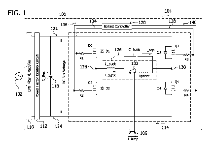
[0024] FIG. 1 is a schematic of a lamp system including a ballast with an
inverter for use
with an input power source to energize a lamp according to embodiments
disclosed herein.
[0025] FIGs. 2A-5B each illustrate exemplary current paths through an inverter
of the ballast
of the lamp system of FIG. 1.
[0026] FIG. 6 is a flow chart illustrating an exemplary sequence of operating
modes
according to embodiments disclosed herein.
DETAILED DESCRIPTION
[0027] FIG. 1 illustrates a lamp system 100 according to embodiments described
herein. The
lamp system 100 includes an input power source 102, such as an alternating
current (AC)
power source, an electronic ballast 104, and a lamp 106. The lamp system 100
described
herein is used to energize, for example, one or more HID lamps 106. Exemplary
HID lamps
include, but are not limited to, mercury vapor, metal halide, high-pressure
sodium, and low-
pressure sodium lamps. The lamp system 100 may be used to energize other types
of lamps,
such as a fluorescent lamp, without departing from the scope of the invention.
[0028] The electronic ballast 104 includes one or more input terminals adapted
to connect to
the input power source 102 and a ground terminal connectable to ground
potential. In some
embodiments, the input power source 102 includes a first voltage source and a
second voltage
source, and the electronic ballast 104 is operatively connected to either the
first voltage
source or the second voltage source. Thus, the electronic ballast 104 may
selectively receive
power from either the first voltage source (e.g., 208 volts AC) or the second
voltage source
(e.g., 347 volts, 480 volts). Other input power sources 102 known in the art
may be used
without departing from the scope of the present invention.
[0029] The electronic ballast 104 receives an input AC power signal from the
input power
source 102 via the input terminal. In some embodiments, the electronic ballast
104 includes
an electromagnetic interference (EMI) filter and a rectifier (e.g., full-wave
rectifier),
illustrated generally at 110. The EMI filter prevents noise, which may be
generated by the
electronic ballast 104, from being transmitted back to the input power source
102. The
rectifier converts AC voltage of the input power signal to DC (direct current)
voltage.
[0030] The electronic ballast 104 includes a power stage to convert power
supplied by the
input power source 102 to drive the lamp 106. In FIG. 1, the electronic
ballast 104 includes a
first power stage comprising a power factor control circuit 112. The power
factor control
circuit 112, such as a boost converter, receives the rectified input power
signal and produces
8
CA 02779911 2012-05-03
WO 2011/071993 PCT/US2010/059423
a high DC voltage (e.g., 460 volts DC). The electronic ballast 104 also
includes a second
power stage comprising a lamp driver (broadly, lamp driver and ignition
circuit) 114. In
particular, as described below, the lamp driver 114 includes an inverter
circuit that converts
the high DC voltage into a suitable AC voltage to energize the lamp 106. A
capacitor 118,
such as an electrolytic capacitor, is connected in a shunt configuration
between the first
power stage (e.g., power factor control circuit 112) and the second power
stage (e.g., lamp
driver 114) to provide a low impedance source of voltage to the inverter. The
electronic
ballast 104 includes a controller 120 (broadly referred to throughout as a
"control circuit") to
control the operations of the components of the electronic ballast 104. In
some embodiments,
the controller 120 has one or more control outputs which electrically connect
the controller
120 to the lamp driver 114. For example, the controller 120 may be a
microcontroller that
may have control outputs that are electrically connected to the lamp driver
114 via driver
control circuits.
[0031] In FIG. 1, the lamp driver (broadly referred to throughout as a "driver
circuit") 114
comprises a first DC voltage bus 122 and a second DC voltage bus 124 (e.g.,
high DC voltage
bus and low DC voltage bus, respectively) connected to the power factor
control circuit 112
and the capacitor 118. A first switching leg and a second switching leg are
each connected
between the first DC voltage bus 122 and the second DC voltage bus 124. The
first switching
leg includes a first switching component Q1 connected to the first DC voltage
bus 122, and a
first diode Dl connected (e.g., shunted) across the first switching component
Q1. The first
switching leg also includes a second switching component Q2 connected between
the first
switching component Q1 and the second DC voltage bus 124, and a second diode
D2
connected (e.g., shunted) across the second switching component Q2. Thus, the
first
switching component Q1 in combination with the first diode Dl is connected in
series with
the second switching component Q2 in combination with the second diode D2.
[0032] Similarly, the second switching leg includes a third switching
component Q3
connected to the first DC voltage bus 122, and a third diode D3 connected
(e.g., shunted)
across the third switching component Q3. The second switching leg also
includes a fourth
switching component Q4 connected between the third switching component Q3 and
the
second voltage bus 124, and a fourth diode connected (e.g., shunted) across
the fourth
switching component Q4. Thus, the third switching component Q3 in combination
with the
third diode D3 is connected in series with the fourth switching component Q4
in combination
with the fourth diode D4. In some embodiments, each of the switching
components Q1, Q2,
9
CA 02779911 2012-05-03
WO 2011/071993 PCT/US2010/059423
Q3, and Q4 is a metal-oxide-semiconductor field-effect transistor (MOSFET).
However, the
scope of the present invention is not limited to a particular type of switch.
[0033] A load circuit 126 connects the first switching leg to the second
switching leg. In
particular, a first inductor Lbu,k is connected to a terminal 128 between the
first switching
component Q1 and the second switching component Q2. A second inductor (e.g.,
igniter) is
connected to a terminal 130 between the third switching component Q3 and the
fourth
switching component Q4. Load terminals 132 are connected between the first
inductor Lbuak
and the second inductor (e.g., igniter) and are adapted for connecting a load,
such as a lamp
106, in series with the first inductor Lbuck and the second inductor (e.g.,
igniter). A capacitor
Cbuck is connected in parallel with the series arrangement of the lamp
terminals 132 and the
second inductor (e.g., igniter).
[0034] As shown in FIG. 1, the controller 120 includes a first control output
134 connected to
the first switching component Q1, a second control output 136 connected to the
second
switching component Q2, a third control output 138 connected to the third
switching
component Q3, and a fourth control output 140 connected to the fourth
switching component
Q4. In operation, the controller 120 operates the first, second, third, and
fourth switching
components Q1, Q2, Q3, Q4 via the first, second, third, and fourth control
outputs 134, 136,
138, 140, respectively, in diagonal pairs in order to convert the high DC
voltage generated by
the power factor control circuit 112 to an AC voltage signal suitable to
energize the lamp
106. The AC voltage signal is comprised of positive cycles and negative
cycles. In
particular, the first switching component Q1 and the fourth switching
component Q4 form a
diagonal pair that is operated to generate the positive cycles of the AC
voltage signal.
Similarly, the second switching component Q2 and the third switching component
Q3 form a
diagonal pair that is operated to generate the negative cycles of the AC
voltage signal.
[0035] Accordingly, the controller 120 is configured to operate the switching
components
Q1, Q2, Q3, and Q4 according to a plurality of operation modes. More
particularly, the
controller 120 is configured to operate the switching components Q1, Q2, Q3,
and Q4 in a
first operation mode for a first time period (e.g., Ti) during which the
current through or
voltage across the first inductor Lbuck has a first polarity (e.g., positive,
negative). The
controller 120 is configured to operate the switching components Q1, Q2, Q3,
and Q4 in a
second operation mode for a second time period (e.g., T2) during which the
current through
or voltage across the first inductor Lbuck has a second polarity (e.g.,
positive, negative) that is
opposite of the first polarity. For example, the first and second operation
modes may be the
positive cycle operation mode and the negative cycle operation mode described
below. The
CA 02779911 2012-05-03
WO 2011/071993 PCT/US2010/059423
controller 120 is configured to operate the switching components Q1, Q2, Q3,
and Q4 in a
third operation mode for a third time period (e.g., T3). The third time period
is a
commutation period during which a polarity of the current through or voltage
across the
capacitor is being reversed. The third time period (e.g., commutation period)
represents a
transition time needed to switch the polarity of the current through or
voltage across the
capacitor Cbõck. Thus, there will be a commutation period each time the
controller 120
transitions from the first time period Ti to the second time period T2 and
from the second
time period T2 back to the first time period Ti.
[0036] More particularly, in some embodiments, the controller 120 is
configured to operate
the switching components in a positive cycle operation mode, a negative cycle
operation
mode, a positive-to-negative transition operation mode, and a negative-to-
positive transition
mode operation. During the positive cycle operation mode, the controller 120
operates the
inverter (i.e., switching components Q1, Q2, Q3, Q4) so that a positive
portion of an AC
voltage signal is provided to the lamp 106. During the negative cycle
operation mode, the
controller 120 operates the inverter (i.e., switching components Q1, Q2, Q3,
Q4) so that a
negative portion of an AC voltage signal is provided to the lamp 106. During
the positive-to-
negative transition operation mode, the controller 120 operates the inverter
(i.e., switching
components Q1, Q2, Q3, Q4) to transition the polarity of the AC voltage signal
provided to
the lamp 106 from positive to negative. Similarly, during the negative-to-
positive transition
operation mode, the controller 120 operates the inverter (i.e., switching
components Q1, Q2,
Q3, Q4) to transition the polarity of the AC voltage signal provided to the
lamp 106 from
negative to positive. The switching sequence described below employed by the
controller
120 during the positive-to-negative transition operation mode and during the
negative-to-
positive transition mode minimizes commutation time. As such, embodiments of
the present
invention reduce Spectral Power Ratio (SPR), re-ignition spikes, poor lumen-
maintenance,
and audible humming noise produced by the lamp 106.
[0037] Referring to FIGs. 2A and 2B, during the positive cycle operation mode,
the
controller 120 operates the inverter (i.e., switching components Q1, Q2, Q3,
Q4) between
two different states. In the first state (i.e., positive cycle state 1),
illustrated in FIG. 2A, the
diagonal pair of switching components comprising the second switching
component Q2 and
the third switching component Q3, is non-conductive. The diagonal pair of
switching
components comprising the first switching component Q 1 and the fourth
switching
component Q4, is conductive. As such, current flows in a path from the first
DC voltage bus
and through the first switching component Q1 and the first inductor Lbõ,k. The
current path
11
CA 02779911 2012-05-03
WO 2011/071993 PCT/US2010/059423
then divides so that current flows through the capacitor Cbuck and the lamp
106 and second
inductor (i.e., igniter). The current path continues through the fourth
switching component
Q4 to the second DC voltage bus. Accordingly, the current through the first
inductor Lbuak
rises and a positive voltage is generated across the lamp 106.
[0038] In the second state during the positive cycle operation mode (i.e.,
positive cycle state
2), illustrated in FIG. 2B, the second switching component Q2 and the third
switching
component Q3 remain non-conductive. The first switching component Q1 is turned
OFF so
that it is non-conductive. Energy stored by the first inductor Lbuck
dissipates to generate a
decreasing current that flows in a closed loop through the capacitor Cbõck,
the lamp 106, and
the second inductor (i.e., igniter) to the fourth switching component Q4, and
then from the
anode to the cathode of the second diode D2. As such, a positive voltage is
maintained
across the lamp 106. When the current through the first inductor Lbuck reaches
zero, the
controller 120 returns the inverter to the positive cycle state 1. As such,
the first switching
component Q1 is turned ON so that it is conductive.
[0039] Subsequent to the positive cycle operation mode, which, in some
embodiments,
includes either positive cycle state 1 or positive cycle state 2, and in other
embodiments,
includes both positive cycle state 1 and positive cycle state 2, the positive-
to-negative
transition mode is initiated. Referring to FIGs. 3A and 3B, during the
positive-to-negative
transition mode, the controller 120 operates the inverter (i.e., switching
components Q1, Q2,
Q3, Q4) between two different states. In the first state (i.e., positive-to-
negative state 1)
illustrated in FIG. 3A, the diagonal pair of switching components comprising
the first
switching component Q1 and the fourth switching component Q4, is non-
conductive. The
diagonal pair of switching components comprising the second switching
component Q2 and
the third switching component Q3, is conductive. As such, current flows in
path from the
first DC voltage bus and through the third switching component Q3. The current
path then
divides so that current flows through capacitor Cbõck, the lamp 106, and the
second inductor
(i.e., igniter). The current path continues through the first inductor Lbõck,
through the second
switching component Q2 to the second DC voltage bus. Accordingly, the current
through the
first inductor Lbuck rises.
[0040] When the current through the first inductor Lbuck reaches a predefined
value (e.g.,
peak value), the second state (i.e., positive-to-negative state 2) of the
positive-to-negative
transition mode is initiated. In the positive-to-negative state 2, illustrated
in FIG. 3B, each of
the switching components Q1, Q2, Q3, and Q4 are non-conductive. As such,
energy stored
by the first inductor Lbuck dissipates to generate a decreasing current that
flows in a path from
12
CA 02779911 2012-05-03
WO 2011/071993 PCT/US2010/059423
the second DC voltage bus and through the fourth diode D4. The current path
divides so that
current flows through the capacitor Cbõck, the lamp 106, and the second
inductor (i.e., igniter).
The current path then continues through the first inductor Lbõ,k, through the
first diode Dl, to
the first DC voltage bus. When the current through the first inductor Lbuk
reaches zero, the
controller 120 returns the inverter to the positive-to-negative state 1.
[0041] Referring to FIGs. 4A and 4B, during the negative cycle operation mode,
the
controller 120 operates the inverter (i.e., switching components Q1, Q2, Q3,
Q4) between
two different states. In the first state (i..e., negative cycle state 1),
illustrated in FIG. 4A, the
diagonal pair of switching components comprising the first switching component
Q1 and the
fourth switching component Q4, is non-conductive. The diagonal pair of
switching
components comprising the second switching component Q2 and the third
switching
component Q3, is conductive. As such, current flows from the first DC voltage
bus and
through the third switching component Q3. The current path then divides so
that current
flows through the capacitor Cbõ,k, the lamp 106, and the second inductor
(i.e., igniter). The
current path continues through the first inductor Lbõ,k, and the second
switching component
Q2 to the second DC voltage bus. Accordingly, the current through the first
inductor Lbuak
rises and a negative voltage is generated across the lamp 106.
[0042] In the second state during the negative cycle operation mode (negative
cycle state 2),
illustrated in FIG. 4B, the first switching component Q1 and the fourth
switching component
Q4 remain non-conductive. The second switching component Q2 is turned OFF so
that it is
non-conductive. Energy stored by the first inductor Lbu,k dissipates to
generate a decreasing
current that flows in a closed loop from the anode to the cathode of the first
diode Dl,
through the third switching component Q3, and then through the capacitor
Cbu,k, the lamp
106, and the second inductor (i.e., igniter). As such, a negative voltage is
maintained across
the lamp 106. When the current through the first inductor Lbu,k reaches zero,
the controller
120 returns the inverter to the negative cycle state 1. As such, the second
switching
component Q2 is turned ON so that it is conductive.
[0043] Subsequent to the negative cycle operation mode, which, in some
embodiments,
includes either negative cycle state 1 or negative cycle state 2, and in other
embodiments,
includes both negative cycle state 1 and negative cycle state 2, the negative-
to-positive
transition mode is initiated. Referring to FIGs. 5A and 5B, during the
negative-to-positive
transition mode, the controller 120 operates the inverter (i.e., switching
components Q1, Q2,
Q3, Q4) between two different states. In the first state (i.e., negative-to-
positive state 1),
illustrated in FIG. 5A the diagonal pair of switching components comprising
the second
13
CA 02779911 2012-05-03
WO 2011/071993 PCT/US2010/059423
switching component Q2 and the third switching component Q3, is non-
conductive. The
diagonal pair of switching components comprising the first switching component
Q1 and the
fourth switching component Q4, is conductive. As such, current flows in path
from the first
DC voltage bus through the first switching component Q1, and through the first
inductor
Lbuek. The current path then divides so that current flows through capacitor
Cbõek, the lamp
106 and the second inductor (i.e., igniter). The current path continues
through the fourth
switching component Q4 to the second DC voltage bus. Accordingly, the current
through the
first inductor Lbuek rises.
[0044] When the current through the first inductor Lbuek reaches a predefined
value (e.g.,
peak value), the second state (i.e., negative-to-positive state 2) of the
negative-to-positive
transition mode is initiated. In the negative-to-positive state 2, illustrated
in FIG. 5B, each of
the switching components Q1, Q2, Q3, and Q4 is non-conductive. As such, energy
stored by
the first inductor Lbuek dissipates to generate a decreasing current that
flows in a path from the
second DC voltage bus, through the second diode D2, and through the first
inductor Lbuek.
The current path is then divided so that current flows through the capacitor
Cbuek, the lamp
106 and the second inductor (i.e., igniter). The current path continues
through the third diode
D3 to the first DC voltage bus. When the current through the first inductor
Lbuek reaches
zero, the controller 120 returns the inverter to the negative-to-positive
state 1.
[0045] FIG. 6 is a flow chart illustrating exemplary operations modes
implemented by the
controller 120 for providing an AC voltage signal to the lamp 106 in
accordance with an
embodiment of the invention. At 202, the controller 120 initiates operation of
the inverter in
the positive cycle operation mode. The positive cycle operation mode has a
predefined
duration period, Tpositive. In an exemplary embodiment, Tposit1Ve has a
predefined value of 3.2
milliseconds. When the positive cycle operation mode is initiated, the
controller 120 operates
the inverter, indicated at 202, in the positive cycle state 1 for a time
period of tposcyclestatel. In
an exemplary embodiment, the time period tposcycle_statel has a pre-defined
value of 5.0 sec.
As indicated at 204 if the time period Tpositive for the positive cycle
operation mode has not
expired, the controller 120 then, at 206, operates the inverter in the
positive cycle state 2 for a
time period of tpos cyclestate2= In an exemplary embodiment, the time period
tpos cycle_state2 has a
pre-defined value of 12.0 sec which is based on the amount of time that it
takes for the
current through the first inductor Lbuek to reach zero. After operating the
inverter in the
positive cycle state 2 for the time period tposcycle state2, the controller
120 returns the inverter
to the positive cycle state 1 at 202. The controller 120 continues to
alternately operate the
inverter between the positive cycle state 1 and the positive cycle state 2 for
the duration of the
14
CA 02779911 2012-05-03
WO 2011/071993 PCT/US2010/059423
positive cycle operation mode time period Tpositive. As such, according to the
exemplary
embodiment, during the positive cycle operation mode, the first switching
component Q1 is
switched at a frequency of 58.8 kHz and the fourth switching component Q4 is
switched at a
frequency of 156.25 Hz.
[0046] When the positive cycle operation mode time period Tpositive expires,
the controller
120 initiates a positive-to-negative transition operation mode. The positive-
to-negative
transition operation mode has a predefined duration period, Tpos_to_1eg. In an
exemplary
embodiment, Tpos_to_1eg has a predefined value of around 46 microseconds. When
the
positive-to-negative transition operation mode is initiated, the controller
120 operates the
inverter, indicated at 208, in the positive-to-negative state 1 for a time
period of tpos_neg states.
The time period tpos_negstatel is a function of the peak value 'MAX for the
current that is passed
through the first inductor Lbuek causing the saturation of the first inductor
Lbuek. In particular
the value of the time period tpos_negstatel is given as follows
LB UCK I MAX
tp s neg-s` `et DC Bus Voltage+Lamp Voltage
[0047] The peak value ImAx for the current is based on the inductance value of
the first
inductor Lbuek. In an exemplary embodiment, the inductance value of the first
inductor Lbuak
is 285 micro Henrys, and the peak value ImAx for the current is accordingly
about 9 Amps. In
the exemplary embodiment, the DC bus voltage is 460 Volts and the lamp voltage
is 135
Volts. As such, in accordance with the exemplary embodiment, the duration for
the positive-
to negative state 1 tpos_negstatel is about 4.3 microseconds.
[0048] As indicated at 210 if the time period Tpos_to_neg for the positive-to-
negative transition
operation mode has not expired, the controller 120 then, at 212, operates the
inverter in the
positive-to-negative state 2 for a time period of tpos_negstate2. In an
exemplary embodiment, the
time period tpos_negstate2 has a pre-defined value of 7.9 tsec, which is based
on the amount of
time that it takes for the current through the first inductor Lbuek to reach
zero. After operating
the inverter in the positive-to-negative state 2 for the time period
tpos_negstate2, the controller
120 returns the inverter to the positive-to-negative state 1 at 208. The
controller 120
continues to alternately operate the inverter between the positive-to-negative
state 1 and the
positive-to-negative state 2 for the duration of the positive-to-negative
transition operation
mode time period Tpos_to_neg.
[0049] When the positive-to-negative transition operation mode time period
Tpos_to_neg expires,
the controller 120 initiates the negative cycle operation mode. The negative
cycle operation
mode has a predefined duration period, Tnegative. In an exemplary embodiment,
Tnegative has a
CA 02779911 2012-05-03
WO 2011/071993 PCT/US2010/059423
predefined value of 3.2 milliseconds. When the negative cycle operation mode
is initiated,
the controller 120 operates the inverter, indicated at 214, in the negative
cycle state 1 for a
time period of tnegcycle statel = In an exemplary embodiment, the time period
tnegcycle_statel has a
pre-defined value of 5.0 tsec. As indicated at 216 if the time period
Tnegative for the negative
cycle operation mode has not expired, the controller 120 then, at 218,
operates the inverter in
the negative cycle state 2 for a time period of tnegcycle_state2. In an
exemplary embodiment, the
time period tõegcycle state2 has a pre-defined value of 12.0 tsec which is
based on the amount of
time that it takes for the current through the first inductor Lbuek to reach
zero. After operating
the inverter in the negative cycle state 2 for the time period tõegcycle
state2, the controller 120
returns the inverter to the negative cycle state 1 at 214. The controller 120
continues to
alternately operate the inverter between the negative cycle state 1 and the
negative cycle state
2 for the duration of the negative cycle operation mode time period Tnegative=
As such,
according to the exemplary embodiment, during the negative cycle operation
mode, the
second switching component Q2 is switched at a frequency of 58.8 kHz and the
third
switching component Q3 is switched at a frequency of 156.25 Hz.
[0050] When the negative cycle operation mode time period Tnegative expires,
the controller
120 initiates negative-to-positive transition operation mode. The negative-to-
positive
transition operation mode has a predefined duration period, T1eg_to_pos. In an
exemplary
embodiment, Tõeg_to_pos has a predefined value of around 46 microseconds. When
the
negative-to-positive transition operation mode is initiated, the controller
120 operates the
inverter, indicated at 220, in the negative-to-positive state 1 for a time
period of tõeg_pos_statei.
The time period tõeg_posstatel is a function of the peak value 'MAX for the
current that is passed
through the first inductor Lbuek causing the saturation of the first inductor
Lbuek. As similarly
described above in connection with the positive-to-negative state 1, the value
of the time
period tõeg_posstatel is given as follows
LBUCKIMAX
tneg-p s statel DC Bus Voltage + Lamp Voltage
[0051] The peak value ImAx for the current is based on the inductance value of
the first
inductor Lbuek. In an exemplary embodiment, the inductance value of the first
inductor Lbuak
is 285 micro Henrys, and the peak value ImAx for the current is accordingly
about 9 Amps. In
the exemplary embodiment, the DC bus voltage is 460Volts and the lamp voltage
is 135
Volts. As such, in accordance with the exemplary embodiment, the duration for
the negative-
to-positive state 1 tõeg_pos_statel is about 4.3 microseconds.
16
CA 02779911 2012-05-03
WO 2011/071993 PCT/US2010/059423
[0052] As indicated at 222 if the time period T1eg_to_pos for the negative-to-
positive transition
operation mode has not expired, the controller 120 then, at 224, operates the
inverter in the
negative-to-positive state 2 for a time period of tpos_negstate2. In an
exemplary embodiment, the
time period tpos_neg_state2 has a pre-defined value of 7.9 tsec, which is
based on the amount of
time that it takes for the current through the first inductor Lbuek to reach
zero. After operating
the inverter in the positive-to-negative state 2 for the time period
tpos_neg_state2, the controller
120 returns the inverter to the positive-to-negative state 1 at 220. The
controller 120
continues to alternately operate the inverter between the negative-to-positive
state 1 and the
negative-to-positive state 2 for the duration of the negative-to-positive
transition operation
mode time period Tneg_to_pos.
[0053] When the negative-to-positive transition operation mode time period
Tneg_to_pos expires,
the controller 120 returns to the positive cycle operation mode. The
controller 120 continues
to cycle through the positive cycle operation mode, positive-to-negative
transition mode,
negative cycle operation mode, and negative-to-positive transition mode as
described above
in order to provide the AC voltage signal to the lamp 106.
[0054] Unless otherwise stated, use of the word "substantially" may be
construed to include a
precise relationship, condition, arrangement, orientation, and/or other
characteristic, and
deviations thereof as understood by one of ordinary skill in the art, to the
extent that such
deviations do not materially affect the disclosed methods and systems.
[0055] Throughout the entirety of the present disclosure, use of the articles
"a" and/or "an"
and/or "the" to modify a noun may be understood to be used for convenience and
to include
one, or more than one, of the modified noun, unless otherwise specifically
stated. The terms
"comprising", "including" and "having" are intended to be inclusive and mean
that there may
be additional elements other than the listed elements.
[0056] Elements, components, modules, and/or parts thereof that are described
and/or
otherwise portrayed through the figures to communicate with, be associated
with, and/or be
based on, something else, may be understood to so communicate, be associated
with, and or
be based on in a direct and/or indirect manner, unless otherwise stipulated
herein.
[0057] Although the methods and systems have been described relative to a
specific
embodiment thereof, they are not so limited. Obviously many modifications and
variations
may become apparent in light of the above teachings. Many additional changes
in the details,
materials, and arrangement of parts, herein described and illustrated, may be
made by those
skilled in the art.
17