Note: Descriptions are shown in the official language in which they were submitted.
CA 02779982 2012-06-15
37719-CA-PAT
MOBILE WIRELESS COMMUNICATIONS DEVICE TO AUTHENTICATE A
= REMOVABLE POWER SOURCE VIA NFC COMMUNICATIONS AND ASSOCIATED
METHODS
Technical Field
[0001] The present disclosure relates to the field of
mobile wireless communications devices, and, more particularly,
to mobile wireless communications devices including Near Field
Communications (NFC) circuits.
Background
[0002] Mobile communication systems continue to grow
in popularity and have become an integral part of both personal
and business communications. Various mobile devices now
incorporate Personal Digital Assistant (PDA) features such as
calendars, address books, task lists, calculators, memo and
writing programs, media players, games, etc. These multi-
function devices also allow users to send and receive electronic
mail (e-mail) messages wirelessly and access the Internet via a
cellular network and/or a wireless local area network (WLAN),
for example. In addition, these devices may allow users to send
Short Messaging Service (SMS) messages, Personal Identification
Number (PIN) messages, and instant messages.
[0003] Given the wide variety of functions now performed by
such mobile wireless communications devices, power consumption
has become an issue. The typical mobile wireless communications
device is now used throughout the day, and not merely for making
and receiving voice calls. As such, manufacturers have invested
considerable money in the design and manufacture of batteries
for their mobile wireless communications devices, and may like a
way to prevent batteries manufactured by third parties from
working with their devices, for a variety of reasons. For
1
= CA 02779982 2012-06-15
=
37719-CA-PAT
example, many mobile wireless communications devices come with a
warranty, and a poorly designed third party battery may damage
the device. Likewise, a poorly designed third party battery may
not allow the device to operate optimally, decreasing a
customer's satisfaction with the device.
[0004] Consequently, a mobile wireless communications device
able to authenticate a battery installed therein is desirable.
Brief Description of the Drawings
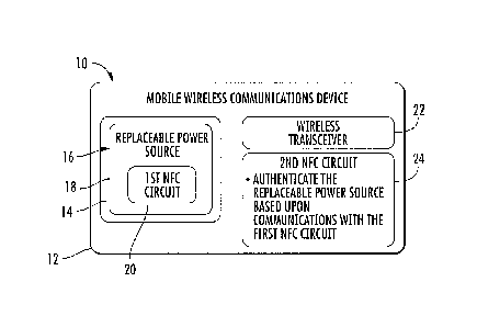
[0005] FIG. 1 is a schematic block diagram of a mobile
wireless communications device in accordance with the present
disclosure.
[0006] FIG. 2 is a schematic block diagram of a more detailed
embodiment of a mobile wireless communications device in
accordance with the present disclosure.
[0007] FIG. 3 is a schematic block diagram of a replaceable
power source powering a mobile wireless communications device in
accordance with the present disclosure.
[0008] FIG. 4 is a flowchart of a method of operating
a mobile wireless communications device in accordance
with the present disclosure.
[0009] FIG. 5 is a high-level block diagram showing
example embodiment additional components that can be used
in the wireless communications device shown in FIG. 1.
Detailed Description
[0010] The present description is made with reference to the
accompanying drawings, in which various embodiments are shown.
However, many different embodiments may be used, and thus the
description should not be construed as limited to the
2
CA 02779982 2012-06-15
=
37719-CA-PAT
embodiments set forth herein. Rather, these embodiments are
provided so that this disclosure will be thorough and complete.
Like numbers refer to like elements throughout, and prime
notation is used to indicate similar elements or steps in
alternative embodiments.
[0011] Generally speaking, a mobile wireless communications
device may comprise a housing, a wireless transceiver carried by
the housing, and a removable power source capable of being
carried by the housing. The removable power source may comprise
a first Near Field Communications (NFC) circuit. A second NFC
circuit may be carried by the housing, and may be configured to
authenticate the removable power source based upon communication
with the first NFC circuit.A processor may be carried by the
housing and may be coupled to the second NFC circuit. The
processor may be configured to switch from a locked state to an
unlocked state based upon a successful authentication of the
removable power source. In addition, the processor may be
configured to switch from an unlocked state to a locked state
based upon an unsuccessful authentication of the removable power
source.
[0012] In some applications, the processor may be configured
to cooperate with the wireless transceiver to place an emergency
call when the processor is switched to a locked state. A display
may be carried by the housing, and the processor may be
configured to cooperate with the display to display an error
message when switched to a locked state.
[0013] The removable power source and the processor may
exchange handshake communications. The handshake communications
may comprise a security code.
[0014] There may be an electrical conduction communication
path between a first processor coupled to the first NFC circuit
and a second processor carried by the housing for additional
3
CA 02779982 2012-06-15
37719-CA-PAT
authentication of the removable power source. The housing may
define a cavity capable of receiving the removable power source,
and the removable power source may be removably positioned
within the cavity.
[0015] The removable power source may further comprise a
sealed battery casing containing the first NFC circuit, and at
least one rechargeable battery cell carried by the sealed
battery casing.
[0016] Another aspect is directed to a removable power source
capable of powering a mobile wireless communications device. The
removable power source may include a first Near Field
Communications (NFC) circuit configured to authenticate the
mobile wireless communications device based upon communication
with a second NFC circuit thereof. The removable power source
may comprise a battery, in some applications. In further
applications, the removable power source may comprise a fuel
cell.
[0017] A method aspect is directed to a method on a mobile
wireless communications device having a housing carrying a
wireless transceiver and a removable power source, the removable
power source comprising a first Near Field Communications (NFC)
circuit. The method may comprise authenticating the removable
power source based upon communications between a second NFC
circuit carried by the housing and the first NFC circuit.
[0018] With initial reference to FIG. 1, a mobile wireless
communications device 10 in accordance with the present
disclosure is now described. Example mobile wireless
communications devices may comprise portable or personal media
players (e.g., MP3 players, video players, electronic book
readers, etc.), remote controls (e.g., television or stereo
remotes, etc.), portable gaming devices, portable or mobile
telephones, smartphones, tablet computers, laptop computers,
4
CA 02779982 2012-06-15
37719-CA-PAT
etc. The mobile wireless communications device 10 includes a
housing 12 that defines a removable power source receiving
cavity 14. A removable power source 16 is removably positioned
within the removable power source receiving cavity 14. The
removable power source 16 may be a rechargeable battery, a fuel
cell or any other form of energy storage or generation system,
for example, and includes a first near field communications
(NFC) circuit 20.
[0019] The mobile wireless communications device 10 also
includes a wireless transceiver 22, such as a cellular
transceiver, and a second NFC circuit 24. The second NFC circuit
24 is configured to authenticate the removable power source 16
based upon communications with the first NFC circuit 20.
[0020] Authenticating the removable power source 16
advantageously allows the manufacturer of the mobile wireless
communications device 10 to ensure that the correct removable
power source 16 is used. For example, there may be removable
power sources 16 that fit within the removable power source
receiving cavity 14, but do pot provide the proper current or
voltage and may degrade the performance or the operability of
the mobile wireless communications device 10. Authentication
would help prevent the incorrect removable power source being
used. In addition, authentication helps prevent unapproved and
potentially dangerous or harmful removable power sources from
being used.
[0021] NFC is a short-range wireless communications
technology in which NFC-enabled devices are "swiped," "bumped"
or otherwise moved in close proximity to communicate. In one
non-limiting example implementation, NFC may operate at 13.56
MHz and with an effective range of several centimeters,
typically 4 cm or less, but other suitable versions of near-
field communication which may have different operating
= CA 02779982 2012-06-15
=
37719-CA-PAT
frequencies, effective ranges, etc., for example, may also be
used.
[0022] Referring now to FIG. 2, a more detailed embodiment of
the mobile wireless communications device 10' is now described.
Here, the removable power source 18' includes at least one
battery cell 17', and a processor 19' coupled to the first NFC
circuit 20'. The battery cell 17' may comprise a rechargeable
lithium-ion cell, for example.
[0023] The mobile wireless communications device 10' also
includes a wireless transceiver 22', input device 26', display
28', and memory 30' coupled to a processor 32'. The memory 30'
may include both volatile portions, such as Random Access Memory
(RAM), and non-volatile portions, such as Flash RAM, in some
applications. The display 28' is typically an Organic Light
Emitting Diode (OLED) display, but may also be a Liquid Crystal
Display (LCD) or other suitable display. The input device 26'
may be a keyboard, touch sensitive pad, trackball, or
thumbwheel, for example. In addition, the input device 26' may
include any number of separate components, such as a keyboard
and a touch sensitive pad. Further, it should be appreciated
that the display 28' may be a touch sensitive display and may
therefore act as at least a portion of the input device 26'. The
wireless transceiver 22' may include a cellular transceiver or a
WLAN transceiver, for example, and the processor 32' may
cooperate with the wireless transceiver for wireless
communications.
[0024] The processor 32' authenticates the removable power
source 16' based upon communications between the second NFC
circuit 24' and first NFC circuit 20'. These NFC communications
may be handshaking communications and may include the exchange
of a security code. For example, during these NFC
communications, the processor 19' may send the security code,
6
CA 02779982 2012-06-15
=
37719-CA-PAT
via the first NFC circuit 20', to the processor 32'. The
processor 32' compares the security code to a stored code to
authenticate the removable power source 16'.
[0025] The processor 32' is switchable between a locked state
and an unlocked state. Generally, when operating in the unlocked
state, the processor 32' performs a variety of device functions.
However, when operating in the locked state, the processor 32'
performs merely a limited number of device functions. For
example, when in the locked state, the processor 32' may display
an error message on the display 28', and may not perform other
device functions regardless of the input received via the input
device 26'.
[0026] Additionally, in some applications when in the locked
state, the processor 32' may permit the placement of an
emergency call (i.e. 911) via the wireless transceiver 22'. The
processor 32' may not perform other device functions, however,
such as messaging and wireless communications, other than
placing the emergency call when in the locked state.
[0027] The processor 32' may switch from the unlocked state
to the locked state based upon an unsuccessful authentication,
and may switch from the locked state to the unlocked state based
upon a successful authentication.
[0028] In some applications, there may be an electrically
conductive communications path 21' between the processor 19' and
the processor 32'. This path permits wired communications
between the processor 19' and the processor 32', and may be used
for additional authentication of the removable power source 16'.
[0029] For example, the processor 32' may generate a
challenge and a response, and then transmit the challenge to the
processor 19' via the electrically conductive communications
path 21'. The processor 19' generates a power source response
and transmits the power source response to the processor 32'
7
CA 02779982 2014-12-09
processor via the electrically conductive communications path
21'. The power source response may be generated based upon a
cryptographic routine. The processor 32' authenticates the
removable power source 16' based upon the power source response
matching a stored response. For further details of this
authentication via the electrically conductive communications
path 21', see U.S. Pat. No. 7,697,957 to Pattenden et al.
[0030] Those elements not specifically discussed are similar
to those of the mobile wireless communications device 10 of FIG.
1 as described above and require no further discussion herein.
[0031] With reference to FIG. 3, another embodiment of the
mobile wireless communications device 10" is now described.
Here, the first NFC circuit 20" is configured to authenticate
the mobile wireless communications device 10" based upon
communications with the second NFC circuit 24". That is, rather
than the processor 32 determining authentication of the mobile
wireless communications device 10" based upon communications
between the first and second NFC circuits 20", 24", the first
NFC circuit determines authentication of the mobile wireless
communications device based upon communications between the
first and second NFC circuits. The first NFC circuit 20" may
then send notice of the authentication to the processor 32" of
the mobile wireless communications device 10".
[0032] Various power saving features may optionally be
implemented by the mobile wireless communications device 10 in
example embodiments. For example, the second NFC circuit 24 may
pulse or scan to detect the first NFC circuit 20 of the
replaceable power source 16 for authentication, e.g., in an
active NFC communication mode. If there is a match (i.e.,
authentication occurs), then there is no need for the second NFC
8
CA 02779982 2012-06-15
37719-CA-PAT
circuit 24 to continue searching or scanning for power source
authentication, and the first NFC circuit 20 may be powered
down, or pulsing may occur at a lower frequency (e.g., to search
for other NFC devices,) etc. For example, a relatively quick
scan from the second NFC circuit 24 to detect the first NFC
circuit 20 may be performed upon being powered up, etc. If there
is a match (i.e., authentication), the second NFC circuit 24 may
switch to a power saving mode (e.g., a passive NFC mode, less
frequent pulses, pulses of shorter duration, etc.). If there is
no authentication, the mobile wireless communications device 10
may be switched to the locked state (e.g., prevented from
booting up upon being powered on), as described further above.
[0033] A method of operating the mobile wireless
communications device 10 (of FIG. 1) is now described with
reference to flowchart 40 of FIG. 4. After the start (Block 42),
the processor 32 authenticates the removable power source 16
based upon handshaking communications between the first and
second NFC circuits 20, 24 (Block 44). At Block 46, if the
removable power source 16 has been authenticated, the processor
32 is switched from the locked state to the unlocked state
(Block 48). If the removable power source 16 has not been
authenticated at Block 46, the processor 32 is switched from the
unlocked state to the locked state (Block 50). The processor 32
may then optionally place an emergency call via the wireless
transceiver 22 (Block 52), or display an error message on the
display (Block 54). Block 56 indicates the end of the method.
[0034] Example components of a mobile wireless communications
device 1000 that may be used in accordance with the above-
described embodiments are further described below with reference
to FIG. 5. The device 1000 illustratively includes a housing
1200, a keyboard or keypad 1400 and an output device 1600. The
output device shown is a display 1600, which may comprise a full
9
= CA 02779982 2012-06-15
=
37719-CA-PAT
graphic LCD. Other types of output devices may alternatively be
utilized. A processing device 1800 is contained within the
housing 1200 and is coupled between the keypad 1400 and the
display 1600. The processing device 1800 controls the operation
of the display 1600, as well as the overall operation of the
mobile device 1000, in response to actuation of keys on the
keypad 1400.
[0035] The housing 1200 may be elongated vertically, or may
take on other sizes and shapes (including clamshell housing
structures). The keypad may include a mode selection key, or
other hardware or software for switching between text entry and
telephony entry.
[0036] In addition to the processing device 1800, other parts
of the mobile device 1000 are shown schematically in FIG. 5.
These include a communications subsystem 1001; a short-range
communications subsystem 1020; the keypad 1400 and the display
1600, along with other input/output devices 1060, 1080, 1100 and
1120; as well as memory devices 1160, 1180 and various other
device subsystems 1201. The mobile device 1000 may comprise a
two-way RF communications device having data and, optionally,
voice communications capabilities. In addition, the mobile
device 1000 may have the capability to communicate with other
computer systems via the Internet.
[0037] Operating system software executed by the processing
device 1800 is stored in a persistent store, such as the flash
memory 1160, but may be stored in other types of memory devices,
such as a read only memory (ROM) or similar storage element. In
addition, system software, specific device applications, or
parts thereof, may be temporarily loaded into a volatile store,
such as the random access memory (RAM) 1180. Communications
signals received by the mobile device may also be stored in the
RAM 1180.
CA 02779982 2012-06-15
37719-CA-PAT
[0038] The processing device 1800, in addition to its
operating system functions, enables execution of software
applications 1300A-1300N on the device 1000. A predetermined set
of applications that control basic device operations, such as
data and voice communications 1300A and 1300B, may be installed
on the device 1000 during manufacture. In addition, a personal
information manager (PIM) application may be installed during
manufacture. The PIM may be capable of organizing and managing
data items, such as e-mail, calendar events, voice mails,
appointments, and task items. The PIM application may also be
capable of sending and receiving data items via a wireless
network 1401. The PIM data items may be seamlessly integrated,
synchronized and updated via the wireless network 1401 with
corresponding data items stored or associated with a host
computer system.
[0039] Communication functions, including data and voice
communications, are performed through the communications
subsystem 1001, and possibly through the short-range
communications subsystem. The communications subsystem 1001
includes a receiver 1500, a transmitter 1520, and one or more
antennas 1540 and 1560. In addition, the communications
subsystem 1001 also includes a processing module, such as a
digital signal processor (DSP) 1580, and local oscillators (L0s)
1601. The specific design and implementation of the
communications subsystem 1001 is dependent upon the
communications network in which the mobile device 1000 is
intended to operate. For example, a mobile device 1000 may
include a communications subsystem 1001 designed to operate with
the MobitexTM, Data TACT"' or General Packet Radio Service (GPRS)
mobile data communications networks, and also designed to
operate with any of a variety of voice communications networks,
such as AMPS, TDMA, CDMA, CDMA, PCS, GSM, EDGE, etc. Other
11
CA 02779982 2012-06-15
37719-CA-PAT
types of data and voice networks, both separate and integrated,
may also be utilized with the mobile device 1000. The mobile
device 1000 may also be compliant with other communications
standards such as 3GSM, 3GPP, UMTS, 4G, etc.
[0040] Network access requirements vary depending upon the
type of communication system. For example, in the Mobitex and
DataTAC networks, mobile devices are registered on the network
using a unique personal identification number or PIN associated
with each device. In GPRS networks, however, network access is
associated with a subscriber or user of a device. A GPRS device
therefore typically involves use of a subscriber identity
module, commonly referred to as a SIM card, in order to operate
on a GPRS network.
[0041] When required network registration or activation
procedures have been completed, the mobile device 1000 may send
and receive communications signals over the communication
network 1401. Signals received from the communications network
1401 by the antenna 1540 are routed to the receiver 1500, which
provides for signal amplification, frequency down conversion,
filtering, channel selection, etc., and may also provide analog
to digital conversion. Analog-to-digital conversion of the =
received signal allows the DSP 1580 to perform more complex
communications functions, such as demodulation and decoding. In
a similar manner, signals to be transmitted to the network 1401
are processed (e.g. modulated and encoded) by the DSP 1580 and
are then provided to the transmitter 1520 for digital to analog
conversion, frequency up conversion, filtering, amplification
and transmission to the communication network 1401 (or networks)
via the antenna 1560.
[0042] In addition to processing communications signals, the
DSP 1580 provides for control of the receiver 1500 and the
transmitter 1520. For example, gains applied to communications
12
CA 02779982 2012-06-15
37719-CA-PAT
signals in the receiver 1500 and transmitter 1520 may be
adaptively controlled through automatic gain control algorithms
implemented in the DSP 1580.
[0043] In a data communications mode, a received signal, such
as a text message or web page download, is processed by the
communications subsystem 1001 and is input to the processing
device 1800. The received signal is then further processed by
the processing device 1800 for an output to the display 1600, or
alternatively to some other auxiliary I/0 device 1060. A device
may also be used to compose data items, such as e-mail messages,
using the keypad 1400 and/or some other auxiliary I/0 device
1060, such as a touchpad, a rocker switch, a thumb-wheel, or
some other type of input device. The composed data items may
then be transmitted over the communications network 1401 via the
communications subsystem 1001.
[0044] In a voice communications mode, overall operation of
the device is substantially similar to the data communications
mode, except that received signals are output to a speaker 1100,
and signals for transmission are generated by a microphone 1120.
Alternative voice or audio I/0 subsystems, such as a voice
message recording subsystem, may also be implemented on the
device 1000. In addition, the display 1600 may also be utilized
in voice communications mode, for example to display the
identity of a calling party, the duration of a voice call, or
other voice call related information.
[0045] The short-range communications subsystem enables
communication between the mobile device 1000 and other proximate
systems or devices, which need not necessarily be similar
devices. For example, the short-range communications subsystem
may include an infrared device and associated circuits and
components, a BluetoothTM communications module to provide for
communication with similarly-enabled systems and devices, or a
13
CA 02779982 2012-06-15
=
=
37719-CA-PAT
near field communications (NFC) sensor for communicating with a
NFC device or NFC tag via NFC communications.
[0046] Many modifications and other embodiments of the
invention will come to the mind of one skilled in the art having
the benefit of the teachings presented in the foregoing
descriptions and the associated drawings. Therefore, it is
understood that the invention is not to be limited to the
specific embodiments disclosed, and that modifications and
embodiments are intended to be included within the scope of the
appended claims.
14