Note: Descriptions are shown in the official language in which they were submitted.
CA 02780434 2012-05-09
1 9 7 P
[DOCUMENT NAME] Description
[Title of Invention] 3 -Level Power Conversion Apparatus
[TECHNICAL FIELD]
[0001]
The present invention relates to a three-level power conversion
apparatus such as an inverter.
[BACKGROUND ART]
[0002]
In the past, as a three-level power conversion apparatus, there has
been known a three-level inverter with three phases which serves to convert a
direct current into an alternating current (for example, see a first patent
document).
In the following, a conventional apparatus described in the first patent
document will be explained with reference to Fig. 9 through Fig. 20. Fig. 9 is
a
circuit diagram which shows a general three-level power conversion apparatus
described in the first patent document, wherein a main circuit construction of
a
three-level inverter with three phases is illustrated.
[0003]
In Fig. 9, the three-level inverter is provided with direct current power
supplies 1, 2 which are connected in series with each other, and which have a
positive side electric potential P (hereinafter referred to as a "P electric
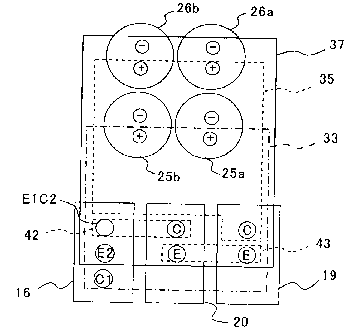
potential"), a negative side electric potential N (hereinafter referred to as
an "N
electric potential"), and a midpoint electric potential M (hereinafter
referred to as
an "M electric potential"). Here, note that in cases where the direct current
power supplies 1, 2 are constructed by an AC power system, in general, a diode
rectifier, an electrolytic capacitor of large capacitance (not shown), etc.
are
used.
[0004]
An IGBT (insulated gate type bipolar transistor) modules 16, 17, 18
(main switches) are connected between the P electric potential and the N
electric potential, and alternating current output terminals (intermediate
terminals) 11 of the individual IGBT modules 16, 17, 18 are connected to the M
electric potential through IGBT modules 19 through 24 (bi-directional
switches),
respectively.
An IGBT (switch element) 3 and a diode 4 in the IGBT module 16 are
connected to the P electric potential, and an IGBT 5 and a diode 6 therein are
1
CA 02780434 2012-05-09
connected to the N electric potential.
[0005]
Each pair of the IGBT modules 19 through 24 construct a bi-directional
switch, which is connected between the M electric potential and each
alternating current output terminal (intermediate terminal) 11 in the IGBT
modules 16 through 18.
The IGBT module 19 is composed of a set of an IGBT 7 and a diode 8
which is connected in anti-parallel to the IGBT 7, and the IGBT module 20 is
composed of a set of an IGBT 9 and a diode 10 which is connected in
anti-parallel to the IGBT 9.
The IGBT modules 19, 20 (bidirectional switch) are of a construction in
which one set of the IGBT and the diode are connected in anti-series to
another
set of the IGBT and the diode, and the IGBT modules 21 through 24, which
correspond to the other two set, are constructed in a similar manner. Here,
note that those IGBTs which are connected in anti-series with each other have
their emitters commonly connected with each other, but they may instead have
their collectors commonly connected with each other.
[0006]
The three-level inverter has its three-phase output terminals connected
to a load 15 through reactors 12, 13, 14 for filtering.
This serves to construct an inverter which can generate an output of
three levels (P electric potential, N electric potential, and M electric
potential).
[0007]
In cases where the three-level inverter of Fig. 9 is constructed by IGBT
modules and direct current power supply devices (electrolytic capacitors of
large capacitance), for example, the IGBT modules 16, 17, 18 are composed of
"2 in 1 type" IGBT modules, respectively, and the IGBT modules 19 through 24
are composed of "1 in 1 type" IGBT modules, respectively, and the direct
current power supplies 1, 2 are composed of serially connected electrolytic
capacitors, respectively. In addition, the IGBT modules 19 through 24 may be
composed of "2 in 1 type" IGBT modules.
[0008]
Fig. 10 is an external appearance perspective view which shows a
construction example of each of the "2 in 1 type" IGBT modules 16 through 18,
and Fig. 11 is an equivalent circuit diagram which shows an internal function
in
Fig. 10.
2
CA 02780434 2012-05-09
In Fig. 10 and Fig. 11, the IGBT module is provided with a collector
terminal (Cl) 27 that is connected to a P electric potential, an emitter
terminal
(E2) 28 that is connected to an N electric potential, and an intermediate
terminal
(emitter/ collector terminal E1C2) 11 that is connected to a load output and a
bi-directional switch. In
general, the individual terminals 27, 28, 11 are
constructed in the order as shown in Fig. 10.
[0009]
Fig. 12 is an external appearance perspective view which shows a
construction example of each of the "1 in 1 type" IGBT modules 19 through 24
(bi-directional switches), and Fig. 13 is an equivalent circuit diagram which
shows an internal function in Fig. 12.
In Fig. 12 and Fig. 13, the IGBT module (bi-directional switch) is
provided with a collector terminal (C) 30 and an emitter terminal (E) 31.
[0010]
On the other hand, Fig. 14 is an external appearance perspective view
which shows a construction example of a "2 in 1 type" bi-directional switch,
and
Fig. 15 is an equivalent circuit diagram which shows an internal function in
Fig.
14.
In Fig. 14 and Fig. 15, IGBT modules (bi-directional switch) are
provided with a collector terminal (Cl) 40 and a collector terminal (C2) 41.
In cases where the IGBT modules 19 through 24 (bi-directional
switches) are composed of modules of the "2 in 1 type", as shown in Fig. 15,
they have a common emitter (or a common collector), and hence, individual
terminals can be constructed as shown in Fig. 14.
[0011]
Fig. 16 is a circuit diagram which shows one phase of the conventional
three-level inverter which is described in the first patent document.
In Fig. 16, the IGBT module 16 and electrolytic capacitors 25, 26 are
connected to each other, at the side of the P potential, by means of a first
conductor 33 which connects between a collector terminal 27 at the side of an
upper arm of the IGBT module 16 and a positive side potential terminal 32 of
the electrolytic capacitors 25, 26.
[0012]
In addition, at the side of the N electric potential, the IGBT module 16
and the electrolytic capacitors 25, 26 are connected to each other by means of
a second conductor 37 which connects between an emitter terminal 28 at the
3
CA 02780434 2012-05-09
side of a lower arm of the IGBT module 16 and a negative side electric
potential
terminal 36 of the electrolytic capacitors 25, 26. At the side of the M
electric
potential, the IGBT module 16 is connected to a series connection point 34 of
the electrolytic capacitors 25, 26 through the IGBT modules 19, 20
(bi-directional switches).
[0013]
Further, the IGBT modules 19, 20 (bi-directional switches) and the
electrolytic capacitors 25, 26 are connected to each other by means of a third
conductor 35 that connects between a collector terminal 30 of the IGBT module
19 and the series connection point 34 of the electrolytic capacitors 25, 26.
[0014]
Fig. 17 through Fig. 19 show the construction of the three-level inverter
(for one phase) of Fig. 16. Fig. 17 is a top plan view which shows a state
seen
from an upper surface thereof. Fig. 18 is a left side view which shows a state
seen from a left side thereof. Fig. 19 is s right side view which shows a
state
seen from a right side thereof.
In Fig. 17 through Fig. 19, in order to distinguish each one pair of series
electrolytic capacitors located at the opposite right and left sides, "a" and
"b" are
attached in such a manner that those electrolytic capacitors which are located
at the right side are denoted by 25a, 26a, and those electrolytic capacitors
which are located at the left side are denoted by 25b, 26b.
[0015]
In Fig. 17 through Fig. 19, the first and the second conductors 33, 37
are arranged in proximity with each other through an insulating material 44.
In addition, an electrically connected two-division conductor 45
(corresponding to the third conductor 35 in Fig. 16) is arranged in the
vicinity of
an anode (series connection point 34) of the electrolytic capacitor 26, and in
the
vicinity of the collector terminal 30 of the IGBT module 19, so that a
proximity
structure is thereby achieved in which the first and the second conductors 33,
37 are sandwiched.
However, insulating materials 46, 48 are interposed between the
two-division conductor 45 and the first conductor 33, and between the
two-division conductor 45 and the second conductor 37, respectively.
[0016]
The individual interconductor distances between the first conductor 33
and the two-division conductor 45, between the second conductor 37 and the
4
CA 02780434 2012-05-09
two-division conductor 45, and between the first conductor 33 and the second
conductor 37, respectively, all become 5 (see Fig. 18), so that a mutual
inductance LM of a large value is generated between the individual conductors.
[0017]
Fig. 20 is an explanatory view which shows mutual inductances LM by
means of an equivalent circuit, wherein in the construction of Fig. 16 through
Fig. 19, it is shown that the mutual inductances LM of the same magnitude are
generated between individual conductors.
In Fig. 20, the two-division conductor 45 as referred to above (Fig. 18
and Fig. 19) is shown as divided into two, i.e., conductors 45a, 45b.
[0018]
The intermediate terminal 11 of the IGBT module 16 and a collector
terminal 30a of the IGBT module 20 are connected to each other by means of a
thin fourth conductor 42 (wiring inductance Lac).
In addition, an emitter terminal 31a of the IGBT module 20 and an
emitter terminal 31b of the IGBT module 19 are connected to each other by
means of a thin fifth conductor 43 (wiring inductance Ls).
[0019]
By forming wiring between the IGBT module 16 and the electrolytic
capacitors 25, 26 into a four-layer laminate structure as in the case of the
above-mentioned conventional three-level power conversion apparatus (Fig. 16
through Fig. 20) as referred to above (the first patent document), it is
possible to
reduce the wiring inductances LM between the IGBT module 19 (bi-directional
switch) and the electrolytic capacitors 25, 26. However,
other wiring
inductances Ls, Lac can not be reduced.
[PRIOR ART REFERENCES]
[PATENT DOCUMENTS]
[0020]
[First Patent Document] Japanese Patent Application Laid-Open No.
2009-22062
[SUMMARY OF THE INVENTION]
[PROBLEMS TO BE SOLVED BY THE INVENTION]
[0021]
Although the conventional three-level power conversion apparatus
reduces the wiring inductances between the IGBT module and the electrolytic
capacitors (direct current power supply) by the use of the four-layer laminate
CA 02780434 2012-05-09
structure as described above, the thickness of the laminate structure is
increased due to the four-layer structure thereof, thus enlarging the size of
the
apparatus thereby to increase the weight thereof as well. In particular, in
the
three-phase three-level power conversion apparatus, there has been a problem
that the amount of increase in weight exerts an influence with its magnitude
becoming about 3 times as large as the original.
In addition, as shown in Fig. 17 through Fig. 20, the intermediate
terminal of the IGBT module 16 and the collector terminal of the IGBT module
20 (bi-directional switch) as well as the emitter terminal 31a of the IGBT
module
20 and the emitter terminal 31b of the IGBT module 19 are connected to each
other by means of the thin conductors 42, 43, respectively, instead of the
laminate structure, and hence, there has been a problem that the wiring
inductances Ls, Lac can not be reduced.
[0022]
The present invention has been made in order to solve the problems as
referred to above, and has for its object to obtain a three-level power
conversion apparatus which is capable of reducing the wiring inductance
between a bi-directional switch part (e.g., the IGBT modules 19 through 24)
and
a main switch part (e.g., the IGBT modules 16 through 18), and which at the
same time is small in size and low in cost.
[MEANS FOR SOLVING THE PROBLEMS]
[0023]
A three-level power conversion apparatus according to the present
invention is provided with: a direct current power supply circuit that has a
positive side terminal; a negative side terminal and an intermediate potential
point; a semiconductor module that is inserted between the positive side
terminal and the negative side terminal; and a bi-directional switch that is
inserted between the intermediate potential point and the semiconductor
module; wherein the semiconductor module is composed of: a first switch
element with a collector thereof connected to the positive side terminal of
the
direct current power supply circuit, and a diode connected in anti-parallel to
the
first switch element; and a second switch element with an emitter thereof
connected to the negative side terminal of the direct current power supply
circuit, and a diode connected in anti-parallel to the second switch element;
and
wherein the bi-directional switch is composed of a series circuit including a
third
bidirectional switch element and a fourth bidirectional switch element that
are
6
CA 02780434 2014-10-03
connected between a connection point of an emitter of the first switch element
and a collector of the second switch element, and the intermediate potential
point of the direct current power supply circuit; and wherein an electric
potential
of three levels is outputted from an output terminal of the semiconductor
module. The three-level power conversion apparatus is further provided with:
a first conductor that makes a connection between the positive side terminal
of
the direct current power supply circuit and the first switch element; a second
conductor that makes a connection between the negative side terminal of the
direct current power supply circuit and the second switch element; a third
conductor that makes a connection between the intermediate potential point of
the direct current power supply circuit and the third switch element; a fourth
conductor that makes a connection between the fourth switch element and the
connection point; and a fifth conductor that makes a connection between the
third switch element and the fourth switch element; wherein the third through
fifth conductors are arranged on a same surface, and the first conductor, the
second conductor and the third through fifth conductors are arranged in a
superposed manner so that a three-layer wiring structure is thereby achieved.
According to an aspect of the present invention, there is provided a three-
level power conversion apparatus comprising:
a direct current power supply circuit that has a positive side terminal, a
negative side terminal and an intermediate potential point;
a semiconductor module that is inserted between said positive side
terminal and said negative side terminal; and
a bi-directional switch that is inserted between said intermediate potential
point and said semiconductor module;
wherein said semiconductor module is composed of:
a first switch element with a collector thereof connected to the positive
side terminal of said direct current power supply circuit, and a diode
connected
in anti-parallel to said first switch element; and
a second switch element with an emitter thereof connected to the negative
side terminal of said direct current power supply circuit, and a diode
connected
in anti-parallel to said second switch element;
wherein said bi-directional switch is composed of a series circuit including
a third switch element and a fourth switch element that are connected between
a connection point of an emitter of said first switch element and a collector
of said
second switch element, and the intermediate potential point of said direct
current
power supply circuit;
7
CA 02780434 2014-10-03
wherein an electric potential of three levels is outputted from an output
terminal of said semiconductor module;
wherein said three-level power conversion apparatus further comprises:
a first conductor that makes a connection between the positive side
terminal of said direct current power supply circuit and said first switch
element;
a second conductor that makes a connection between the negative side
terminal of said direct current power supply circuit and said second switch
element;
a third conductor that makes a connection between the intermediate
potential point of said direct current power supply circuit and said third
switch
element;
a fourth conductor that makes a connection between said fourth switch
element and said connection point; and
a fifth conductor that makes a connection between said third switch
element and said fourth switch element;
wherein said third conductor, said forth conductor and said fifth conductor
are arranged on a single surface;
wherein said first conductor, said second conductor and said third
conductor, said fourth conductor and said fifth conductor are arranged in a
superposed manner on said semiconductor module and said bi-directional switch
so that a three-layer wiring structure is thereby achieved, and
said third conductor, said fourth conductor and said fifth conductor are
separate and are arranged between said first and second conductors, and at the
same time, said third conductor, said fourth conductor and said fifth
conductor
are disposed between insulating materials to form a close contact structure.
According to another aspect of the present invention, there is provided a
three-level power conversion apparatus comprising:
a direct current power supply circuit that has a positive side terminal, a
negative side terminal and an intermediate potential point,
a semiconductor module that is inserted between said positive side
terminal and said negative side terminal; and
a bi-directional switch that is inserted between said intermediate potential
point and said semiconductor module;
wherein said semiconductor module is composed of:
7a
CA 02780434 2014-10-03
a first switch element with a collector thereof connected to the positive
side terminal of said direct current power supply circuit, and a diode
connected
in anti-parallel to said first switch element; and
a second switch element with an emitter thereof connected to the negative
side terminal of said direct current power supply circuit, and a diode
connected
in anti-parallel to said second switch element;
wherein said bi-directional switch is composed of a series circuit including
a third switch element and a fourth switch element that are connected between
a connection point of an emitter of said first switch element and a collector
of said
second switch element, and the intermediate potential point of said direct
current
power supply circuit;
wherein an electric potential of three levels is outputted from an output
terminal of said semiconductor module;
wherein said three-level power conversion apparatus further comprises:
a first conductor that makes a connection between the positive side
terminal of said direct current power supply circuit and said first switch
element;
a second conductor that makes a connection between the negative side
terminal of said direct current power supply circuit and said second switch
element;
a third conductor that makes a connection between the intermediate
potential point of said direct current power supply circuit and said series
circuit;
and
a fourth conductor that makes a connection between said series circuit
and said connection point;
wherein said third and fourth conductors are arranged on a single surface;
wherein said first conductor, said second conductor and said third and
fourth conductors are arranged in a superposed manner on said semiconductor
module and said bi-directional switch so that a three-layer wiring structure
is
thereby achieved; and
wherein said third switch element and said fourth switch element are
arranged inside a same package, and
said third and fourth conductors are separate and are arranged between
said first and second conductors, and, said third and fourth conductors are
disposed between insulating materials to form a close contact structure.
7b
CA 02780434 2014-10-03
[EFFECT OF THE INVENTION]
[0024]
According to the present invention, by arranging a divided conductor at
an intermediate potential side between a first conductor at a positive side,
and a
second conductor at a negative side in such a manner that the first conductor,
the second conductor and the divided conductor are arranged in a superposed
manner so as to form a three-layer wiring structure, it becomes possible to
provide a circuit in which the wiring inductance between the bi-directional
switch
part and the main switch part is reduced, and which at the same time is small
in
size and low in cost due to the three-layer wiring structure having a small
number of laminated layers.
[BRIEF DESCRIPTION OF THE DRAWINGS]
[0025]
[Fig. 1] is a top view which shows a state in which one phase of a
three-level power conversion apparatus according to a first embodiment of the
present invention is seen from an upper surface thereof. (First Embodiment)
[Fig. 2] is a left side view which shows a state in which the three-level
power conversion apparatus in Fig. 1 is seen from a left side thereof. (First
Embodiment)
7c
CA 02780434 2012-05-09
[Fig. 3] is a right side view which shows a state in which the three-level
power conversion apparatus in Fig. 1 is seen from a right side thereof. (First
Embodiment)
[Fig. 4] is an equivalent circuit diagram which shows wiring inductances
between individual conductors in Fig. 1 through Fig. 3. (First Embodiment)
[Fig. 5] is a top view which shows a state in which one phase of a
three-level power conversion apparatus according to a second embodiment of
the present invention is seen from an upper surface thereof. (Second
Embodiment)
[Fig. 6] is a left side view which shows a state in which the three-level
power conversion apparatus in Fig. 5 is seen from a left side thereof. (Second
Embodiment)
[Fig. 7] is a right side view which shows a state in which the three-level
power conversion apparatus in Fig. 5 is seen from a right side thereof.
(Second Embodiment)
[Fig. 8] is an equivalent circuit diagram which shows wiring inductances
between individual conductors in Fig. 5 through Fig. 7. (Second Embodiment)
[Fig. 9] is a circuit diagram which shows a main circuit construction of a
general three-level inverter.
[Fig. 10] is an external appearance perspective view which shows a
conventional "2 in 1 type" IGBT module.
[Fig. 11] is an equivalent circuit diagram which shows an internal
function of the IGBT module in Fig. 10.
[Fig. 12] is an external appearance perspective view which shows a
conventional "1 in 1 type" IGBT module.
[Fig. 13] is an equivalent circuit diagram which shows an internal
function of the IGBT module in Fig. 12.
[Fig. 14] is an external appearance perspective view which shows a
conventional "2 in 1 type" bi-directional switch module.
[Fig. 15] is an equivalent circuit diagram which shows an internal
function of the bi-directional switch module in Fig. 14.
[Fig. 16] is a circuit diagram which shows one phase of a conventional
three-level inverter.
[Fig. 17] is a top plan view which shows a state in which one phase of
the conventional three-level inverter in Fig. 16.
[Fig. 18] is a left side view which shows a state in which the three-level
8
CA 02780434 2012-05-09
inverter in Fig. 17 is seen from a left side thereof.
[Fig. 19] is a right side view which shows a state in which the three-level
inverter in Fig. 17 is seen from a right side thereof.
[Fig. 20] is an equivalent circuit diagram which shows wiring
inductances between individual conductors in Fig. 17 through Fig. 19.
[MODES FOR CARRYING OUT THE INVENTION]
[0026]
(First Embodiment)
Fig. 1 is a top plan view which shows a three-level power conversion
apparatus according to a first embodiment of the present invention, wherein a
state in which one phase of three phases thereof is seen from an upper surface
thereof is shown. Fig. 2 is a left side view which shows a state in which the
three-level power conversion apparatus in Fig. 1 is seen from a left side
thereof,
and Fig. 3 is a right side view which shows a state in which the three-level
power conversion apparatus in Fig. 1 is seen from a right side thereof.
In addition, Fig. 4 is an equivalent circuit diagram which shows one
phase of the three-level power conversion apparatus shown in Fig. 1 through
Fig. 3.
Here, note that the overall construction of the three-level power
conversion apparatus according to the first embodiment of the present
invention is as shown in Fig. 9.
[0027]
In Fig. 1 through Fig. 4, those which are similar to the above-mentioned
ones (see Fig. 17 through Fig. 20) are denoted by the same reference numerals
and characters as those referred to above.
The one phase of the three-level power conversion apparatus is
provided with an IGBT module 16 that has a collector terminal Cl, an emitter
terminal E2 and an emitter/ collector terminal E1C2, IGBT modules 19, 20
(bi-directional switch) that have collector terminals (C) 30b, 30a and emitter
terminals (E) 31b, 31a, respectively, and electrolytic capacitors 25 (25a,
25b)
and electrolytic capacitors 26 (26a, 26b) that which constitute direct current
power supplies, respectively.
[0028]
As shown in Fig. 4, the IGBT module 16 is composed of a first switch
element 3 that has a collector terminal (Cl) 27 connected to a positive side
terminal (+) (P electric potential) of an electrolytic capacitor 25, a diode 4
that is
9
CA 02780434 2012-05-09
connected in anti-parallel to the first switch element 3, a second switch
element
that has an emitter terminal (E2) 28 connected to a negative side terminal (-)
(N electric potential) of an electrolytic capacitor 26, and a diode 6 that is
connected in anti-parallel to the second switch element 5.
The intermediate terminal 11 (the emitter/ collector terminal E1C2) of
the IGBT module 16 is connected to the IGBT modules 19, 20 (bi-directional
switch), and at the same time is connected to a load 15 (see Fig. 9) through a
reactor 12 for filtering.
[0029]
A connection point between the first switch element 3 and the diode 4 in
the IGBT module 16 and between the second switch element 5 and the diode 6
therein is connected to a series connection point of the electrolytic
capacitors
25, 26 through the IGBT modules 19, 20 (bi-directional switch).
The IGBT module 19 has a third switch element 7, and the IGBT
module 20 has a fourth switch element 9. The IGBT modules 19, 20
(bi-directional switch) are composed of a series circuit of the third switch
element 7 and the fourth switch element 9.
[0030]
The collector terminal (Cl) 27 of the IGBT module 16 and the positive
side terminal (+) of the electrolytic capacitor 25 are electrically connected
to
each other by means of a first conductor 33 (wiring inductance Lp).
In addition, the emitter terminal (E2) 28 of the IGBT module 16 and the
negative side terminal (-) of the electrolytic capacitor 26 are electrically
connected to each other by means of a second conductor 37 (wiring inductance
Ln).
[0031]
The collector terminal (C) 30b of the IGBT module 19 (bi-directional
switch), and the series connection point of the electrolytic capacitors 25, 26
(between a cathode of the electrolytic capacitor 25 and an anode of the
electrolytic capacitor 26) are electrically connected to each other by means
of a
third conductor 35 (wiring inductance Lm).
In addition, the intermediate terminal (E1C2) 11 of the IGBT module 16
and the collector terminal (C) 30a of the IGBT module 20 (bi-directional
switch)
are electrically connected to each other by means of a fourth conductor 42
(wiring inductance Lac).
Moreover, the emitter terminal (C) 31a of the IGBT module 20
CA 02780434 2012-05-09
(bi-directional switch) and the emitter terminal (E) 31b of the IGBT module 19
(bi-directional switch) are electrically connected to each other by means of a
fifth conductor 43 (wiring inductance Ls).
[0032]
The third through the fifth conductors 35, 42, 43 are arranged on the
same surface, as shown in Fig. 1 through Fig. 3.
In addition, as shown in Fig. 2 and Fig. 3, the third conductor 35 is
arranged between the first conductor 33 and the second conductor 37, and the
fourth and the fifth conductors 42, 43 are sandwiched by insulating materials
38,
39 so as to form a close contact structure. Here, the insulating material 39
is
interposed between the third conductor 35 (lying on the same plane as the
fourth and the fifth conductors 42, 43) and the first conductor 33, and the
insulating material 38 is interposed between the third conductor 35 and the
second conductor 37. According to this, wiring of a three-layer laminate
structure is formed.
[0033]
Here, note that in Fig. 1 through Fig. 4, the first through the fifth
conductors 33, 37, 35, 42, 43 related to the IGBT module 16 for one phase
have been shown, but it is assumed that the same wiring or connection
structure is also provided in each of the IGBT modules 17, 18 (see Fig. 9) of
the
other two phases.
In addition, in Fig. 1 through Fig. 3, there is shown an example in which
"the first conductor 33", "the third through the fifth conductors 35, 42, 43
arranged on the same surface", and "the second conductor 37" are laminated in
this order from the lower layer side, but they are not limited to such a
laminate
structure.
For example, they may be laminated in such a manner that the first
conductor 33 is placed between the second conductor 37 and the third through
the fifth conductors 35, 42, 43, or they may be laminated such that the second
conductor 37 is placed between the first conductor 33 and the third through
the
fifth conductors 35, 42, 43.
[0034]
Moreover, in the above-mentioned description, there has been shown
the IGBT module 16 for one phase alone, but it goes without saying that the
same structure is provided for each of the IGBT modules 17, 18 (see Fig. 9) of
the other two phases.
11
CA 02780434 2012-05-09
That is, as shown in Fig. 9, similarly to the case where corresponding to
the first IGBT module 16, the first IGBT modules 19, 20 (bi-directional
switches)
are connected thereto, a second and a third IGBT module (bi-directional
switch)
are also connected to the second and the third IGBT module 17, 18 (not shown
in Fig. 1 through Fig. 4), respectively.
[0035]
As described above, the three-level power conversion apparatus
according to the first embodiment of the present invention (Fig. 1 through
Fig. 4)
is provided with the electrolytic capacitors 25, 26 (direct current power
supply
circuit) that each have a positive side terminal (P, +), a negative side
terminal (N,
-) and an intermediate potential point (M), the IGBT module 16 (17, 18) that
is
inserted between the positive side terminal (+) and the negative side terminal
(-),
and the IGBT modules 19, 20 (bi-directional switch) that are inserted between
the intermediate potential point (M) and the IGBT module 16 (17, 18), wherein
the IGBT module 16 (17, 18) of each phase has the first switch element 3 with
its collector connected to the positive side terminal (+) of the electrolytic
capacitor 25, and the second switch element 5 with its emitter connected to
the
negative side terminal (-) of the electrolytic capacitor 26, and wherein an
electric potential of three levels is outputted from an output terminal of the
IGBT
module 16 (17, 18).
[0036]
The IGBT modules 19, 20 (bi-directional switch) is composed of a
series circuit which comprises the third bidirectional switch element 7 and
the
fourth bidirectional switch element 9 that are connected between a connection
point (intermediate terminal 11) of the emitter of the first switch element 3
and
the collector of the second switch element 5, and the intermediate potential
point (M) of the electrolytic capacitors 25, 26.
[0037]
In addition, the three-level power conversion apparatus is further
provided with: the first conductor 33 that makes a connection between the
positive side terminal (+) of the electrolytic capacitor 25 and the first
switch
element 3; the second conductor 37 that makes a connection between the
negative side terminal (-) of the electrolytic capacitor 26 and the second
switch
element 5; and the third through the fifth conductors 35, 42, 43 (three-
divided
conductor) that make connections between the intermediate potential point of
the electrolytic capacitors 25, 26 and the third and the fourth switch
elements 7,
12
CA 02780434 2012-05-09
9, respectively.
[0038]
The third conductor 35 makes a connection between the intermediate
potential point of the electrolytic capacitors 25, 26 (direct current power
supply
circuit) and the third switch element 7. The fourth conductor 42 makes a
connection between the fourth switch element 9 and the connection point (the
intermediate terminal 11). The fifth conductor 43 makes a connection between
the third switch element 7 and the fourth switch element 9.
The third through the fifth conductors 35, 42, 43 are arranged on the
same surface, and the first conductor 33, the second conductor 37 and the
three-divided third through fifth conductors 35, 42, 43 are arranged in a
superposed manner so as to achieve a three-layer wiring structure.
In this manner, by forming the three-layer wiring structure with a small
number of layers, it is possible to achieve the three-level power conversion
apparatus which is small in size and low in cost.
[0039]
Moreover, in the wiring or interconnection structure between the
electrolytic capacitors 25, 26 (direct current power supplies) and the IGBT
module 16 (17, 18), a wiring conductor for an intermediate potential part of
the
electrolytic capacitors 25, 26 is formed by the third through the fifth
conductors
35, 42, 43 which are divided into three pieces on the same surface, and
further,
the third through the fifth conductors 35, 42, 43 are sandwiched by the first
and
the second conductors 33, 37 at the PN (positive and negative pole) sides, and
at the same time are formed into a close contact structure through the
insulating
materials 38, 39.
[0040]
According to such a construction, the wiring inductance Lm between
the electrolytic capacitors 25, 26 (direct current power supplies) and the
IGBT
module 16 (17, 18) can be reduced, and at the same time, the wiring
inductances Ls, Lac, which have not been able to be reduced with the
conventional apparatus (Fig. 17 through Fig. 20), can also be reduced.
[0041]
(Second Embodiment)
Here, note that in the above-mentioned first embodiment (Fig. 1
through Fig. 4), the IGBT modules 19, 20 (the third and the fourth switch
elements 7, 9), which construct a bi-directional switch, are formed into
13
CA 02780434 2012-05-09
individual separate circuits from each other, but as shown in Fig. 5 through
Fig.
8, there may be used an IGBT module 49 (bi-directional switch) of a single
construction in which the third and the fourth switch elements 7, 9 are
unified or
integrated with each other inside a package.
[0042]
Fig. 5 is a top plan view which shows a three-level power conversion
apparatus according to a second embodiment of the present invention, wherein
a state in which one phase of three phases thereof is seen from an upper
surface thereof is shown, similarly as mentioned above. Fig. 6 is a left side
view which shows a state in which the three-level power conversion apparatus
in Fig. 5 is seen from a left side thereof, and Fig. 7 is a right side view
which
shows a state in which the three-level power conversion apparatus in Fig. 5 is
seen from a right side thereof.
In addition, Fig. 8 is an equivalent circuit diagram which shows one
phase of the three-level power conversion apparatus shown in Fig. 5 through
Fig. 7.
Here, note that the overall construction of the three-level power
conversion apparatus according to the second embodiment of the present
invention is as shown in Fig. 9.
[0043]
In Fig. 5 through Fig. 8, those which are similar to the above-mentioned
ones (see Fig. 1 through Fig. 4) are denoted by the same reference numerals
and characters as those referred to above.
The IGBT module 49 (bi-directional switch) in Fig. 5 and Fig. 8 is
composed of the same "2 in 1 type" IGBT module as mentioned above in Fig.
14 and Fig. 15, and is provided with a collector terminal (Cl) 40 and a
collector
terminal (C2) 41.
The left side view (Fig. 6) of Fig. 5 is the same as that of Fig. 2.
[00441
As shown in Fig. 5 through Fig. 8, the three-level power conversion
apparatus is provided with: a first conductor 33 that serves to electrically
connect a positive side terminal (+) of an electrolytic capacitor 25 (25a,
25b)
and a collector terminal (Cl) 27 of an IGBT module 16 to each other; a second
conductor 37 that serves to electrically connect a negative side terminal 36
of
an electrolytic capacitor 26 (26a, 26b) and an emitter terminal (E2) 28 of the
IGBT module 16 to each other; a third conductor 35 that serves to electrically
14
CA 02780434 2012-05-09
connect a negative pole or cathode (-) of the electrolytic capacitor 25 and a
positive pole or anode (+) of the electrolytic capacitor 26 to the collector
terminal (Cl) 40 of the IGBT module 49 ("2 in 1 type" bi-directional switch);
and
a fourth conductor 42 that serves to electrically connect the collector
terminal
(C2) 41 of the IGBT module 49 and an intermediate terminal (E1C2) 11 of the
IGBT module 16 to each other.
[0045]
Similarly as stated above, the first conductor 33, the second conductor
37, and the third and the fourth conductors 35, 42 are arranged in a
superposed
manner so as to form a close contact structure, as a result of which wiring of
a
three-layer laminate structure is constructed.
Here, note that in Fig. 5 through Fig. 7, there is shown an example in
which the first conductor 33, the third and the fourth conductors 35, 42
arranged
on the same surface, and the second conductor 37 are laminated in this order,
but the first conductor 33 is not limited to this.
For example, the first conductor 33 may be laminated in such a manner
that the first conductor 33 is placed between the second conductor 37 and the
third and the fourth conductors 35, 42, or it may be laminated such that the
second conductor 37 is placed between the first conductor 33 and the third and
the fourth conductors 35, 42.
[0046]
By forming the three-layer wiring structure as shown in Fig. 5 through
Fig. 8, it becomes possible to provide a circuit which is small in size and
low in
cost, similarly as stated above.
In addition, the wiring of the three-layer laminate structure is
constructed by placing the third and the fourth conductors 35, 42 on the same
surface, and also placing the third and the fourth conductors 35, 42 between
the
first conductor 33 and the second conductor 37, and further placing or
sandwiching the third and the fourth conductors 35, 42 between the insulating
materials 38, 39 so as to form the close contact structure.
[0047]
Moreover, as shown in Fig. 8, by using the IGBT module 49 ("2 in 1
type" bi-directional switch) in which the third and the fourth switch elements
7, 9
are unified or integrated with each other inside the same package, it is
possible
to reduce the wiring inductance Lm between the electrolytic capacitors 25, 26
(direct current power supplies) and the IGBT module 16 (17, 18), and at the
CA 02780434 2012-05-09
same time, to reduce the wiring inductance Lac between the IGBT module 49
and the IGBT module 16, which have not been able to be reduced with the
conventional apparatus (Fig. 17 through Fig. 20).
[0048]
As described above, in the three-level power conversion apparatus
according to the second embodiment of the present invention (Fig. 5 through
Fig. 8), in place of the IGBT modules 19,20 as mentioned above (Fig. 1 and
Fig.
4), the IGBT module 49 (the "2 in 1 type" bi-directional switch), in which the
third
and the fourth switch elements 7, 9 are unified or integrated with each other,
is
inserted between a connection point (intermediate terminal 11) of an emitter
of
the first switch element 3 and a collector of the second switch element 5, and
an
intermediate potential point (M) of the electrolytic capacitors 25, 26.
[0049]
In addition, the three-level power conversion apparatus is further
provided with: the first and the second conductors 33, 37 similar to those as
mentioned above; the third conductor 35 that makes a connection between the
intermediate potential point of the electrolytic capacitors 25, 26 and the
IGBT
module 49 (the third and the fourth switch elements 7, 9); and the fourth
conductor 42 that makes a connection between the IGBT module 49 and the
intermediate terminal 11 of the IGBT module 16 (the first and the second
switch
elements 3, 5).
[0050]
The first conductor 33, the second conductor 37, and the third and the
fourth conductors 35, 42 (two-divided conductor) are of the three-layer wiring
structure through the insulating materials 38, 39, and are arranged in a
superposed manner. That is, between the first conductor 33 and the second
conductor 37, the third and the fourth conductors 35, 42 are sandwiched by the
insulating materials 38, 39, so that the close contact structure and the
three-layer wiring structure are thereby achieved.
[0051]
Thus, in the wiring structure between a direct current power supply
circuit (the electrolytic capacitors 25, 26) and the IGBT module 16 (17, 18)
of
each phase, it is constructed such that a wiring conductor for the
intermediate
potential part of the electrolytic capacitors 25, 26 is divided into two
conductors
on the same surface, and these conductors are sandwiched by the first and the
second conductors 33, 37 at the PN (positive and negative pole) sides.
16
CA 02780434 2012-05-09
According to such a construction, similarly as mentioned above, with the
wiring
structure having a small number of layers, it is possible to achieve the
three-level power conversion apparatus which is able to reduce wiring
inductances between the direct current power supplies and the modules and
which is small in size and low in cost.
[0052]
Here, note that in the above-mentioned first and second embodiments,
the description has been made by taking the case of the three-level power
conversion apparatus of three phases as a three-level power conversion
apparatus, but it goes without saying that the present invention can also be
applied to a three-level power conversion apparatus of a single phase, and
operational effects equivalent to those as mentioned above will be attained.
In addition, although the IGBT module 16 (17, 18) has been used as a
semiconductor module which constructs a main switch part, there may be used
other semiconductor modules such as a MOSFET, etc.
[EXPLANATION OF REFERENCE NUMERALS AND CHARACTERS]
[0053]
3 first switch element, 5 second switch element, 7 third switch
element, 9 fourth switch element, 4, 6 diodes, 11 intermediate terminal
(alternating current output terminal), 15 load, 16 through 18 IGBT modules,
19 through 24, 49 IGBT modules (bi-directional switches), 25, 25a, 25b, 26,
26a, 26b electrolytic capacitors (direct current power supply circuit), 33
first
conductor, 35 third conductor, 37 second conductor, 42 fourth conductor,
43 fifth conductor, 38, 39 insulating materials, Lp, Lm, Ln, Lac, Ls wiring
inductances.
17