Note: Descriptions are shown in the official language in which they were submitted.
CA 02781663 2012-05-23 111005:911017
DESCRIPTION
TITLE OF INVENTION
Semiconductor Thin-Film Manufacturing Method, Semiconductor Thin-Film
Manufacturing Apparatus, Susceptor, and Susceptor Holder
TECHNICAL FIELD
The present invention relates to a method for manufacturing a semiconductor
thin-film, an apparatus for manufacturing a semiconductor thin-film, a
susceptor, and a
susceptor holder. In particular, the present invention relates to
semiconductor thin-
film manufacturing method and manufacturing apparatus based on the CVD
(Chemical
Vapor Deposition) method that epitaxially grows a single-crystal semiconductor
thin-
film on a susceptor, and further relates to the susceptor and a susceptor
holder used for
the manufacturing apparatus.
BACKGROUND ART
A semiconductor substrate for which SiC (silicon carbide) is used has a higher
bandgap and superior characteristics such as thermal resistance and thermal
conductivity, as compared with a semiconductor substrate for which Si
(silicon) is used.
Thus, studies of the former semiconductor substrate are being actively
conducted.
For manufacture of this semiconductor substrate made of SiC (hereinafter
referred to as "SiC substrate"), a hot-wall CVD apparatus has conventionally
been used.
As to manufacture of an SiC substrate by means of this hot-wall CVD apparatus,
a description will be given with reference to Fig. 12. Fig. 12 is a diagram
schematically showing main components of a conventional hot-wall CVD
apparatus.
In Fig. 12, a substrate 10 is of single crystal and serves as a seed substrate
for
epitaxially growing SiC.
Further, a susceptor 20 is provided for mounting substrate 10 thereon, made of
C (carbon) coated with SiC or TaC (tantalum carbide) or the like, and caused
to heat up
by high-frequency induction heating by means of a work coil 70 located below,
and
-1-
CA 02781663 2012-05-23 111005:911017
thereby heat substrate 10.
Furthermore, a heating plate 30 is placed opposite to susceptor 20, made
similarly to susceptor 20, namely made of C coated with SiC or TaC or the
like, and
caused to heat up through high-frequency induction heating by a work coil 32
located
above. Here, this apparatus is further provided with heat insulating materials
31, 60,
shield plates (shields) 33, 71 made of stainless steel, cooling pipes 34, 72,
a quartz pipe
80, an apparatus wall 90, a gas inlet 95, and a gas outlet 96.
Into the apparatus in which the temperature is set to 1500 to 1600 C and the
vacuum is set to 13.3 to 26.6 kPa (100 to 200 Ton), a source gas of SiH4 and
C3Hs and
a carrier gas of H2 are introduced from gas inlet 95 and accordingly, on a
surface of
substrate 10 mounted on susceptor 20, SiC single crystal is epitaxially grown.
After
this, the gases are discharged from gas outlet 96 to the outside of the
apparatus.
This hot-wall system, however, involves the following problems. Specifically,
the introduced source gas forms the SiC single crystal on substrate 10, and
also forms
polycrystalline SiC on a surface of heating plate 30 which is placed opposite
to
substrate 10. The polycrystalline SiC formed on heating plate 30 forms
particles that
could fall on substrate 10 on which the SiC single crystal has been grown. If
the SiC
single crystal is mixed with the polycrystalline SiC, the quality of the SiC
substrate will
be degraded. It has therefore been necessary to regularly clean the inside of
the
apparatus for preventing the particles from falling.
Further, in the case where a plurality of substrates 10 are to be mounted on
susceptor 20 with the aim of improving the production efficiency, if six
substrates of
around 50 mm (two inches) in diameter for example are to be disposed, a
susceptor of a
considerably large size is unnecessary. If, however, six substrates of around
150 mm
(six inches) in diameter are to be disposed, a susceptor of a very large size
is required.
Such a susceptor having a large size also has a large surface area, which
involves a
further problem that heat is likely to be lost due to radiation and
accordingly the energy
cost is increased.
-2-
CA 02781663 2012-05-23 111005:911017
In order to overcome these problems, a technique has been disclosed (Japanese
Patent Laying-Open No. 2008-311542 (PTL 1)). Specifically, a plurality of
plates on
which substrates are mounted are installed in multiple stages, so that the
surface area of
the susceptor per unit volume is reduced. Accordingly, efficient heating is
performed
with reduced heat loss, and the space is also saved. Further, the plates are
arranged in
such a manner that an upper plate extends more upstream of the gas flow than a
lower
plate. In this way, this technique prevents SiC particles from falling on the
substrate
and forms epitaxial films on many substrates.
A technique is also disclosed according to which a plurality of susceptors on
which substrates are mounted are arranged in multiple stages and multiple sets
of
source gas inlets and outlets are provided in different directions, to thereby
form
epitaxial films on many substrates (Japanese Patent Laying-Open No. 2009-
158726
(PTL 2)).
CITATION LIST
PATENT LITERATURE
PTL 1: Japanese Patent Laying-Open No. 2008-3 1 1 542
PTL 2: Japanese Patent Laying-Open No. 2009-158726
SUMMARY OF INVENTION
TECHNICAL PROBLEM
Regarding the technique disclosed in Japanese Patent Laying-Open No. 2008-
311542, however, a greater substrate size causes a difference between the
composition
of the upstream gas and the composition of the downstream gas, which results
in a
difference in the quality and the thickness and also a difference in the
impurity
concentration between the epitaxial films. Thus, products of a stable quality
are
difficult to obtain. Further, although this technique prevents adhesion of
particles, it
does not prevent generation itself of the particles.
Regarding the technique disclosed in Japanese Patent Laying-Open No. 2009-
158726, while multiple sets of source gas inlets and outlets are provided,
there is a
-3-
111005: 911017
CA 02781663 2012-05-23
limitation in the number of sets, and therefore, respective lengths of source
gas paths
cannot be made equal to each other. In addition, the gas flow is disturbed.
Accordingly, uniform epitaxial films cannot be obtained. In the case where the
source
gas that has not been heated sufficiently arrives on each substrate, the
temperature of
the gas continues increasing even on the substrate, which causes a
distribution of the
epitaxial film thickness and a distribution of the impurity concentration, and
accordingly uniform epitaxial films fail to be obtained.
Thus, there has been a demand for development of the technique of preventing
particle generation and accordingly producing epitaxial films in high volume
that are of
excellent uniformity in the quality, the thickness and further the impurity
concentration
for example, while eliminating waste of energy.
SOLUTION TO PROBLEM
A semiconductor thin-film manufacturing method of the present invention
includes the following steps.
Substrates are mounted on a plurality of susceptors respectively. The
plurality
of susceptors on which the substrates are mounted respectively are placed on a
rotational mechanism, so that the susceptors are vertically spaced at a
predetermined
interval. The rotational mechanism on which the plurality of susceptors are
placed is
rotated. The plurality of susceptors on which the substrates are mounted
respectively
are heated. Semiconductor thin-films are deposited by supplying a source gas
to each
of the susceptors that are heated while being rotated, the source gas having
been heated
while passing through gas flow paths of respective path lengths substantially
equal to
each other.
This manufacturing method uses a plurality of susceptors on which substrates
are mounted to form a large number of semiconductor substrates (wafers)
simultaneously, and thus can exhibit excellent mass productivity.
Further, since a plurality of susceptors are vertically spaced at a
predetermined
interval, waste of energy can be eliminated.
-4-
111005: 911017
CA 02781663 2012-05-23
Furthermore, since the source gas having been heated to a temperature close to
a
predetermined film-deposition temperature while passing through gas flow paths
of
respective path lengths substantially equal to each other is introduced into
each gap
between the plurality of susceptors, the sufficiently-heated source gas is
introduced
under the same conditions to the susceptors regardless of the vertical
position of the
susceptor. Therefore, epitaxial films that are uniform in terms of the
quality, the
thickness, and further the impurity concentration can be formed on the
substrates,
regardless of the vertical position. Moreover, since the substrates are
rotated by the
rotational mechanism, the source gas introduced onto the susceptor can be
distributed
uniformly across the whole substrate surface. Consequently, epitaxial films
can be
formed that are excellent in uniformity of the thickness for example. The
uniformity
is achieved not only among the substrates but also within a substrate.
As to the multiple-stage arrangement, an example experiment was conducted by
the inventors of the present invention. Specifically, in the case where a
hydrogen-
based gas of 100 slm was flown, the amount of heat was about 13 kW for a
single
susceptor arranged in a single stage, while the amount of heat was about 7 kW
for
susceptors arranged in multiple stages. Thus, it has been confirmed that the
multiple-
stage arrangement can reduce the amount of heat to approximately one half.
The source gas may be supplied in a form of a laminar flow to each of the
plurality of susceptors.
The laminar flow of the source gas can be used to introduce to each susceptor
the sufficiently-heated source gas under the same conditions regardless of the
vertical
position of the susceptor.
Specifically, a plurality of stationary rectifying plates provided at the same
intervals as the intervals between the susceptors for example can be arranged
immediately before the susceptors which are heated while being rotated, to
allow the
source gas to pass and thereby produce a laminar flow of the source gas.
The step of mounting substrates may include the step of placing the substrates
-5-
CA 02781663 2012-05-23 111005:911017
on both sides respectively of at least one of a plurality of susceptors.
Since substrates (single-crystal substrates) are disposed on both sides
respectively of the susceptor, the source gas flows between substrates
opposite to each
other, so that a uniform single-crystal film can be formed on each of the
substrates.
Consequently, polycrystal can be prevented from being formed on the susceptor
and
particle generation can be prevented. Since uniform single-crystal films can
be
formed respectively on both sides of the susceptor, the mass productivity is
further
enhanced.
At least one of: the plurality of susceptors; and the source gas, may be
heated
with radiant heat from a plurality of surfaces generated by resistance
heating.
In the case where induction heating is employed as a heating method, if the
rotational mechanism is introduced like the present invention, the symmetry of
the path
in which induction current flows is broken and induction heating is also
performed
asymmetrically. Therefore, a temperature distribution is generated and uniform
heating fails to be performed. Moreover, induction current could flow in the
rotational
mechanism and partial over-heating could occur.
In contrast, the resistance heating method is heating by radiation from a
heater.
Therefore, these problems will not occur and uniform heating can easily be
performed
without temperature distribution. Further, heating is performed from at least
two sides
such as the upper side and the lower side, the asymmetry of the heat
homogenizer plate
which heats the susceptors can be compensated for to reduce the temperature
distribution of the heat homogenizer plate.
The resistance heating may be performed by a plurality of resistance heaters
controlled independently of each other.
Heating by the resistance heater can be performed while balancing the applied
power based on independent temperature control to thereby compensate for the
asymmetry of the heat loss from the rotational mechanism and perform uniform
heating.
The above-described induction heating method requires a plurality of expensive
-6-
CA 02781663 2012-05-23 111005:911017
power supplies for performing independent temperature control. Further, in the
case
where the induction heating method is used to perform heating from two sides,
interference of high frequencies from the high-frequency coils occurs, and
therefore,
independent control is difficult to perform. The resistance heating method
involves
none of these problems.
At least one of: the plurality of susceptors; and the source gas may be heated
by
high-frequency heating. Thus, heating can be done in a short period and
therefore the
production efficiency of the semiconductor thin-films can be improved.
A plurality of susceptors each may have an outer periphery with a rotational
peripheral velocity of not higher than a velocity of flow of the source gas
supplied to
the plurality of susceptors.
The rotational peripheral velocity of the outer periphery of the susceptors
can be
controlled so that it is equal to or lower than the velocity of flow of the
source gas, and
the source gas can be flown in the form of a laminar flow. Further, in the
case where a
stationary rectifying plate is provided before the susceptor, the stationary
rectifying
plate can keep the laminar flow of the source gas generated by the stationary
rectifying
plate. On the substrate, an epitaxial film can thus be formed that is
excellent in
uniformity of the thickness, quality, the impurity concentration and the like.
The step of placing the plurality of susceptors on the rotational mechanism
may
include the step of loading the plurality of susceptors into a chamber (55)
containing the
rotational mechanism. The plurality of susceptors may be unloaded after the
step of
depositing semiconductor thin-films. In each of the step of loading the
plurality of
susceptors and the step of unloading the plurality of susceptors, an ambient
temperature
in the chamber may be kept at not less than 200 C.
When the susceptors are loaded/unloaded in an ambient of a low temperature
close to the room temperature, a temperature difference between an increased
temperature and a decreased temperature causes thermal expansion and
contraction
based on which stress is generated. Accordingly, polycrystalline SiC for
example that
-7-
CA 02781663 2012-05-23 111005:911017
has adhered to the susceptor, the gas inlet and the rectifying plate for
example other
than the substrate peels off which could generate particles.
The ambient temperature can be kept at 200 C or more to prevent the adhering
matter from peeling off and prevent particle generation. Further, at such a
temperature,
moisture does not adhere to the substrate. Therefore, particle generation due
to the
moisture can also be prevented. The ambient temperature is more preferably 300
C or
more.
Since the above-described induction heating method is high-frequency heating,
if the susceptor is moved while a high-frequency voltage is applied, high-
frequency
could be mismatched. Therefore, when the susceptor is to be removed, the high-
frequency heating has to be rendered off. A constant temperature is thus
difficult to
keep. In contrast, in the case where resistance heating is used, a constant
temperature
can be kept by applying electrical energy.
The manufacturing method may further include the step of unloading the
plurality of susceptors having a temperature of not less than 700 C, after the
step of
depositing semiconductor thin-films. Thus, the manufacturing efficiency of the
semiconductor thin-films is further improved.
The step of depositing semiconductor thin-films may be performed by
depositing one of silicon carbide and nitride.
Since the wide-bandgap semiconductors such as silicon carbide or nitride
semiconductor have a large coupling energy, the source gas must be heated
sufficiently
for depositing a film of the semiconductor. In the present invention as
described
above, the source gas having been heated sufficiently can be supplied between
rotating
susceptors, which is suitable as a method for manufacturing these wide-bandgap
semiconductors.
A semiconductor thin-film manufacturing apparatus of the present invention
forms a semiconductor thin-film by supplying a source gas onto a substrate,
and
includes a plurality of susceptors, a rotational mechanism, a heating
mechanism, and a
-8-
CA 02781663 2012-05-23 111005:911017
source gas introduction mechanism. The plurality of susceptors (20-22) are
mounted
with substrates respectively. On the rotational mechanism, the plurality of
susceptors
are placed so that the susceptors are vertically spaced at a predetermined
interval, and
the rotational mechanism rotates the plurality of susceptors. The heating
mechanism
heats the plurality of susceptors each and the source gas to a predetermined
temperature.
The source gas introduction mechanism supplies, to the plurality of susceptors
each, the
source gas having been heated while passing through gas flow paths of
respective path
lengths substantially equal to each other.
The semiconductor thin-film manufacturing apparatus configured in the above-
described manner can provide semiconductor in high volume on which respective
epitaxial films are formed that are excellent in uniformity of characteristics
such as
quality, thickness, and impurity concentration, not only among the substrates
but also
within a substrate, as described above.
Further, since a plurality of susceptors are vertically spaced at a
predetermined
interval, heating can efficiently be performed with reduced energy waste, as
described
above, and the apparatus can be made compact.
The source gas introduction mechanism may include a laminar flow forming
mechanism causing the source gas supplied to the plurality of susceptors each,
to flow
in a form of a laminar flow.
For example, a plurality of stationary rectifier plates provided at the same
intervals as the intervals between the susceptors may be arranged immediately
upstream
of the susceptors which are heated while being rotated, to thereby form a
laminar flow
of the source gas. Accordingly, as described above, the sufficiently-heated
source gas
can be introduced under respective conditions identical to each other to the
susceptors,
regardless of the vertical position of the susceptor.
The heating mechanism may include a resistance heater. The resistance heater
may be configured to be capable of emitting radiant heat from a plurality of
surfaces.
The radiant heat from the resistance heater can be used to easily generate a
-9-
111005: 911017
CA 02781663 2012-05-23
uniform heating state without problems such as asymmetrical heating in the
case where
the induction heating method is used as described above.
The above-described manufacturing apparatus may further include a metal
chamber and a heat insulating material. The chamber is water-cooled and
contains the
resistance heater. The heat insulating material is placed between the
resistance heater
and the chamber.
Since the resistance heater is contained in the water-cooled metal chamber,
the
chamber can be prevented from being heated and control of heating is
facilitated. As a
result, the safety can be improved. Further, the source gas can be prevented
from
leaking to thereby avoid waste of the source gas.
Since the resistance heater is contained with the heat insulating material
between the chamber and the heater, heat from the resistance heater can be
enclosed in
a certain environment to thereby achieve efficient heating.
Further, the resistance heater with which the space can be saved is used, the
heater is contained in the water-cooled metal chamber with the heat insulating
material
therebetween, and further, the rotational mechanism on which the susceptors
are
vertically arranged at predetermined intervals is employed. Thus, a more
compact
semiconductor thin-film manufacturing apparatus can be provided.
In the case of high-frequency heating (induction heating method), high
frequency would be induced in the metal chamber. Therefore, the heating unit
is
difficult to be contained in the metal chamber. Thus, in this case, a quartz
pipe or
quartz window is generally used that is less safe than the water-cooled metal
chamber.
The heating mechanism may be a high-frequency heating mechanism.
The above-described manufacturing apparatus may further include a rotational
drive shaft for transmitting a drive force to the rotational mechanism. The
rotational
drive shaft may be made of carbon and have a diameter of not less than 5 mm
and not
more than 20 mm.
The above-described manufacturing apparatus may further include a lifting and
-10-
CA 02781663 2012-05-23 111005:911017
lowering mechanism for lifting and lowering the plurality of susceptors.
A susceptor of the present invention is used for the above-described
manufacturing apparatus, and includes a plate-shaped body and a latch
protrusion.
The plate-shaped body is provided with a hole (20b) formed so that the
substrate can be
mounted. The latch protrusion protrudes from the plate-shaped body toward the
inside
of the hole for preventing the substrate from dropping off the hole.
The susceptor of such a simple configuration can be used to easily arrange two
substrates in one susceptor and simultaneously form upper and lower epitaxial
films,
and accordingly, the mass productivity is considerably improved.
Specifically, a first one of the substrates is first placed in the hole of the
susceptor so that the front side of the first substrate faces downward. Then,
the spacer
is placed and further a second one of the substrates is placed so that the
front side of the
second substrate faces upward. At this time, the latch protrusions are
provided in at
least three locations along the lower inner wall surface of the susceptor, and
therefore,
these substrates and spacer will not drop off. The two substrates can thus be
disposed.
A susceptor holder of the present invention is used for the rotational
mechanism
of the semiconductor thin-film manufacturing apparatus described above. The
susceptor holder holds the plurality of susceptors each in such a manner that
the
plurality of susceptors are vertically spaced at a predetermined interval. A
protrusion
is provided on a head of the susceptor holder so that the protrusion can be
used for
loading and unloading a plurality of susceptors.
While all susceptors are held vertically at predetermined intervals, the
susceptors are uniformly rotated. Accordingly, semiconductor films without
dispersion of features such as thickness can be formed on each of the
substrates placed
in the susceptors.
Further, in this state, the susceptors can be loaded and unloaded. Therefore,
the susceptors can be loaded and unloaded easily at an ambient temperature of
200 C or
more as described above. Specifically, a T-shaped protrusion is provided on
the head
-11-
111005: 911017
CA 02781663 2012-05-23
of the susceptor holder, and an arm holds this protrusion therein to load and
unload the
susceptors.
ADVANTAGEOUS EFFECTS OF INVENTION
The present invention can prevent particle generation and thus manufacture,
with a compact apparatus, epitaxial films in high volume that have excellent
uniformity
in terms of characteristics such as quality, thickness, and impurity
concentration, not
only among the substrates but also within a substrate, while eliminating waste
of the
energy and the source gas.
BRIEF DESCRIPTION OF DRAWINGS
Fig. 1 is a cross section generally and schematically showing a semiconductor
thin-film manufacturing apparatus in a first embodiment of the present
invention.
Fig, 2 is a diagram schematically showing a chamber and its vicinity of the
semiconductor thin-film manufacturing apparatus in the first embodiment of the
present
invention.
Fig. 3 shows a diagram (A) schematically illustrating main components of the
chamber of the semiconductor thin-film manufacturing apparatus in the first
embodiment of the present invention, and an enlarged view (B) of a part of the
diagram.
Fig. 4 is a diagram conceptually showing a state where a source gas is
uniformly
supplied.
Fig. 5 is a diagram schematically illustrating introduction of a source gas to
susceptors of the semiconductor thin-film manufacturing apparatus in the first
embodiment of the present invention.
Fig. 6 shows an exploded perspective view (A) generally and schematically
showing an example intermediate susceptor of the semiconductor thin-film
manufacturing apparatus in the first embodiment of the present invention, and
a cross
section (B) of the susceptor.
Fig. 7 shows an exploded perspective view (A) generally and schematically
showing another example intermediate susceptor of the semiconductor thin-film
-12-
CA 02781663 2012-05-23 111005:911017
manufacturing apparatus in the first embodiment of the present invention, and
a cross
section (B) of the susceptor.
Fig. 8 is a perspective view generally and schematically showing the lowermost
susceptor of the semiconductor thin-film manufacturing apparatus in the first
embodiment of the present invention.
Fig. 9 is provided for illustrating the effects of substrate rotations and
source-
gas preheating, and shows a graph (A) illustrating an example relation between
the
distance in the flow direction of the source gas and the thickness of the
semiconductor
thin-film, and a graph (B) illustrating an example relation between the
distance in the
flow direction of the source gas and the temperature of the source gas.
Fig. 10 is a partial cross section generally and schematically showing a
semiconductor thin-film manufacturing apparatus in a second embodiment of the
present invention.
Fig. 11 is a perspective view generally showing a high-frequency heating unit
in
Fig. 10 and its vicinity.
Fig. 12 is a diagram showing a state where SiC semiconductor substrates of a
comparative example are manufactured.
DESCRIPTION OF EMBODIMENTS
In the following, the present invention will be described specifically based
on
embodiments.
First Embodiment
1. Semiconductor thin-film manufacturing apparatus
(1) Overall configuration
First, the whole of a CVD apparatus (hereinafter also referred to as
"apparatus")
provided as a semiconductor thin-film manufacturing apparatus in the present
embodiment will be described using Figs. 1 and 2. Here, Fig. 1 is a cross
section
generally and schematically showing the semiconductor thin-film manufacturing
apparatus in the present embodiment, and Fig. 2 is a diagram schematically
showing a
-13-
CA 02781663 2012-05-23
111005:911017
chamber and its vicinity that is a main component of the semiconductor thin-
film
manufacturing apparatus.
As shown in Figs. 1 and 2, the semiconductor thin-film manufacturing apparatus
in the present embodiment includes a chamber 55 made of SUS, a rotational
mechanism 50 for rotating substrates, a gas inlet 95 from which a source gas
is
introduced, a preheating unit 77 heating the source gas in advance, a turbo-
molecular
pump 97 and an exhaust duct 98 for exhausting gas, and a glove box 52 and a
pass box
54 for removing epitaxially-grown substrates.
Preheating unit 77 is designed to have a predetermined length so that the
introduced gas is uniformly and sufficiently heated. Further, in order to
introduce the
source gas under the same conditions to respective spaces between the
susceptors, the
preheating unit is designed to have a larger cross section than a set of
susceptors
disposed in the vertical direction and fixed by a susceptor holder.
In chamber 55 in which a water cooling jacket 42 is provided along the top and
bottom inner wall, a heater 76 of the resistance heating type surrounded with
a heat
insulating material 75 formed of carbon felt is provided. A susceptor is set
between
two heaters 76 provided above and below the susceptor respectively.
(2) Chamber
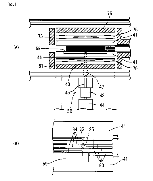
Next, a configuration in chamber 55 will be described using Fig. 3 (A) and
Fig.
3 (B). Fig. 3 (A) and Fig. 3 (B) schematically show main components of the
chamber.
As shown in Fig. 3 (A), heat homogenizer plates 41 are provided so that each
plate contacts heater 76 surrounded with heat insulating material 75. Lower
heat
homogenizer plate 41 is provided with a rotational plate 59. On rotational
plate 59,
susceptors are arranged. Rotational plate 59 is connected to a rotational
shaft 46 of
rotational mechanism 50. Rotational shaft 46 has an upper part formed of a
carbon
rod 40, is connected via a quartz joint 47 to a shaft 45 made of SUS, and
further
connected to a motor 44 via a magnetic fluid seal 43. Namely as motor 44
rotates,
rotational plate 59 rotates via magnetic fluid seal 43.
-14-
111005: 911017
CA 02781663 2012-05-23
The susceptor also serves as a rotational rectifier plate 94, and is placed in
the
vicinity of a stationary rectifier plate 93 in such a manner that the
rotational rectifier
plate and the stationary rectifier plate form the same horizontal plane. This
state is
shown in Fig. 3 (B). The rectifier plates generate a laminar flow of the
introduced
source gas, and this source gas of substantially the same temperature is
uniformly
introduced to each susceptor. Rotational rectifier plates 94 (susceptors) are
secured to
each other by a susceptor holder 25 so that they rotate together as a set of
susceptors.
Thus, susceptor holder 25 is used for rotational mechanism 50. Susceptor
holder 25 holds each of a plurality of susceptors (rotational rectifier plates
94) so that
the susceptors are vertically spaced at predetermined intervals. Susceptor
holder 25
has its head provided with a protrusion 85 so that it can be used for loading
and
unloading a plurality of susceptors.
Fig. 4 conceptually shows the state where the source gas is uniformly
supplied.
In Fig. 4, except for the top and bottom substrates, substrates 11, 12 are
placed on one
susceptor with a spacer 13 therebetween. Since the source gas is introduced
from gas
inlet 95 through the long preheating unit (not shown) to each space between
the
susceptors under the same conditions such as temperature and velocity of flow,
epitaxial films are formed respectively on the substrates under the same
conditions.
Further, since the susceptors are rotating, the source gas can uniformly be
distributed
over the whole surface of each substrate. As a result, the epitaxial films can
be formed
that are excellent in uniformity in characteristics such as thickness,
quality, and
impurity concentration. The uniformity is exhibited not only among the
substrates but
also within each substrate.
Further, as shown in Fig. 3 (B), since stationary rectifier plate 93 is
provided
before each susceptor, the source gas in the form of a laminar flow is
introduced to each
susceptor. Accordingly, the epitaxial films that are more excellent in
uniformity can
be formed.
(3) Susceptor
-15-
CA 02781663 2012-05-23 111005:911017
Next, the susceptor will be described using Figs. 5, 6 (A), 6 (B), 7 (A), and
7
(B).
Fig. 5 is a diagram schematically illustrating introduction of the source gas
to
the susceptors, and corresponds to the conceptual diagram of Fig. 4. In the
manufacturing apparatus of the present embodiment, the flow of the source gas
is
controlled by a rectifier unit 100. Rectifier unit 100 includes susceptors 20
to 22 and a
plurality of stationary rectifier plates 93. To susceptors 20 to 22 that are
rotating with
substrates 12 placed thereon, the source gas is introduced via stationary
rectifier plates
93, and a single crystal is epitaxially grown on the substrate placed in each
susceptor.
In Fig. 5, as to intermediate susceptor 20, two substrates, namely upper and
lower
substrates are placed in the susceptor. As to lowermost susceptor 21, only its
upper
surface has a substrate placed thereon. As to uppermost susceptor 22, only its
lower
surface has a substrate placed thereon.
A plurality of stationary rectifier plates 93 are arranged correspondingly to
susceptors 20 to 22, respectively. A height HS of the space between susceptors
21 and
22 is almost equal to a height HI of the space between the lowermost
stationary rectifier
plate 93 and the uppermost stationary rectifier plate 93. For example, height
HI is
within 10% of height HS.
Next, in Fig. 6 (A) and Fig. 6 (B), a perspective view and a cross section
generally showing intermediate susceptor 20 are given respectively. As shown
in Fig.
6 (A) and Fig. 6 (B), intermediate susceptor 20 includes a disklike susceptor
body 20a
having a predetermined thickness. In susceptor body 20a, a hole 20b is formed
for
setting substrates 11, 12 therein. Latch protrusions 20c protruding from body
20a
toward the inside of hole 20b are provided in at least three locations
respectively.
Here, as shown in Fig. 7 (A) and Fig. 7 (B), latch protrusion 20c may also be
provided
in the form of a ring along the whole inner circumference of the lower part of
susceptor
body 20a.
In hole 20b of horizontally-set susceptor 20, a first substrate 11 is placed
so that
-16-
CA 02781663 2012-05-23 111005:911017
the front side of the substrate faces downward. Then, spacer 13 is placed on
substrate
11, and a second substrate 12 is further placed on the spacer so that the
front side of the
substrate faces upward. The material for spacer 13 is preferably the same as
the
material for the susceptor, and the thickness of spacer 13 is defined so that
the sum of
the thickness of the spacer and respective thicknesses of the two substrates
is equal to
the thickness of the susceptor. In this way, each substrate surface and the
corresponding susceptor surface can be laid in the same plane.
Since hole 20b in which the substrates are set is provided with latch
protrusions
20c at three or more locations, the two substrates will not fall even when the
susceptor
is lifted.
How a substrate is set in lowermost susceptor 21 is shown in Fig. 8. Since the
lower surface of lowermost susceptor 21 abuts on the rotational plate, only
one
substrate is set here. In the upper surface of susceptor 21, a counter bore
21b is
provided instead of through hole 20b (Fig. 6 (A)). In the lower surface of
susceptor 22
as well, a similar counter bore is provided.
2. Manufacture (epitaxial growth) of semiconductor thin-film on substrate
Next, a description will be given of manufacture (epitaxial growth) of a
semiconductor thin film using the above-described apparatus.
Initially, two substrates are set in each susceptor (one substrate in an
uppermost/lowermost susceptor). A plurality of susceptors in which the
substrates are
set are fixed at predetermined intervals in the vertical direction by means of
the
susceptor holder (a set of susceptors), and thereafter the susceptors are
transported into
the chamber and attached to the rotational plate.
Next, the turbo-molecular pump is used to exhaust a residual gas in the
chamber,
the glove box, and the pass box so that a high vacuum is generated therein.
Then, while the set of susceptors is rotated by the rotational mechanism, the
inside of the chamber is heated to a predetermined temperature by the heaters.
After this, a source gas is introduced from the gas inlet into the chamber. At
-17-
CA 02781663 2012-05-23 111005:911017
this time, the source gas has sufficiently been heated in advance by the
preheating unit.
After the source gas is flown, a dry pump is used instead of the turbo-
molecular pump
to exhaust the gas from the exhaust duct.
The heated source gas is introduced via the stationary rectifier plates to the
rotational rectifier plates (susceptors). At this time, since the preheating
unit is
designed so that it has a greater size than the set of susceptors, the source
gas is
introduced to each stationary rectifier plate and each susceptor under the
same
conditions. Further, since the source gas is fed through the stationary
rectifier plates,
the source gas flows in the form of a laminar flow. The rotational peripheral
velocity
of the outer periphery of the susceptor is controlled so that the velocity is
equal to or
lower than the velocity of flow of the source gas. Accordingly, the laminar
flow of the
source gas is not disturbed and flows between the rotating susceptors.
The uniform source gas thus introduced allows a single crystal to epitaxially
grow on each substrate that is excellent in uniformity of characteristics such
as film
quality, film thickness, and impurity concentration.
Here, as to an influence of the heating state of the source gas on the film
thickness, a description will be given based on Fig. 9 (A) and Fig. 9 (B). In
Fig. 9 (A)
and Fig. 9 (B) each, the horizontal axis represents the position along the
direction of the
flow of the source gas. The vertical axis in Fig. 9 (A) represents the
thickness of a
semiconductor thin-film formed on a substrate, and the vertical axis in Fig. 9
(B)
represents the gas temperature on the substrate.
In the case where the gas has been heated sufficiently, the gas of a constant
temperature is introduced onto the substrate as indicated by the solid line in
Fig. 9 (B).
As for the film thickness in this case, the thickness gradually decreases as
the gas is
consumed if the substrate is not rotated, as indicated by the alternate long
and short
dash line in Fig. 9 (A). In the case where the substrate is rotated, the film
with a
uniform thickness is deposited as indicated by the solid line in Fig. 9 (A).
In contrast, in the case where the gas has not been heated sufficiently, the
film
-18-
111005: 911017
CA 02781663 2012-05-23
of a sufficient thickness cannot be deposited initially even if the substrate
is rotated, as
indicated by the broken line in Fig. 9 (B). In the region of the edge and its
vicinity of
the substrate, the thickness of the film also decreases as the gas is
consumed.
After a single-crystal film of a predetermined thickness is formed, the set of
susceptors is unloaded at a temperature of 200 C or more into the glove box of
an inert
gas ambient such as Ar gas. The susceptor set is unloaded at a high
temperature to
thereby prevent moisture from adhering to components such as susceptor,
heater, and
heat homogenizer plate, and enable subsequent high-purity epitaxial films to
be formed.
Further, since the rate of decrease of the temperature from around 200 C is
smaller, the
susceptor set can be unloaded and the subsequent susceptor set can be loaded
at such a
high temperature to thereby increase the throughput of the apparatus.
Further, the temperature in the chamber is not lowered to a temperature close
to
the room temperature, to thereby enable particles from being generated due to
peeling
of adhering matters caused by a temperature change.
The susceptor set having been unloaded at a high temperature is cooled in the
glove box to the room temperature. After this, the set is let fall in the pass
box and
removed so that the atmosphere does not enter the glove box.
In each of the manufacture steps described above, the heaters are thermally
insulated by the carbon-felt heat insulating material, and therefore, the heat
loss is small
in each step. Further, since the components to be heated are surrounded with
the
water cooling jacket, the apparatus can be downsized. Moreover, the
temperature
increase in the room in which the apparatus is installed can be made minimum.
In accordance with the present embodiment, while the source gas is heated to a
temperature close to the susceptor temperature before reaching the group of
substrates,
the source gas is fed through the flow paths to respective substrates, and the
flow paths
have respective lengths substantially equal to each other. Thus, the
dispersion of
respective temperatures of the source gas when it reaches respective
substrates is small.
In this way, the dispersion of respective film-deposition conditions for the
substrates
-19-
CA 02781663 2012-05-23 111005:911017
can be reduced.
Here, the fact that respective lengths of the paths of the source gas are
substantially equal to each other specifically means that the path lengths are
substantially equal to each other in terms of heating of the source gas, and
corresponds
for example to the fact that the dispersion of respective path lengths for the
substrates is
within 10% relative to a certain value.
Second Embodiment
Referring to Figs. 10 and 11, a semiconductor thin-film manufacturing
apparatus in the present embodiment includes a quartz pipe 255 (chamber), a
high-
frequency coil 274, heat insulating materials 275, 276, and 276v, a carbon rod
240,
high-frequency heating units 241 a and 241 b, a rotational drive shaft 245, a
rotational
direction changing unit 247, a transport arm 265, and a lifting and lowering
mechanism
257. Lifting and lowering mechanism 257 has a control rod 258 and a
displacement
rod 250.
Rotational drive shaft 245 is made of carbon and may have a diameter D of not
less than 5 mm and not more than 20 mm. Rotational drive shaft 245 is rotated
about
its axis to transmit a drive force. The drive force transmitted by rotational
drive shaft
245 is changed in its rotational direction by rotational direction changing
unit 247 into a
rotational force of carbon rod 240 functioning as a rotational mechanism.
In the present embodiment, susceptors 20 to 22 and a plurality of stationary
rectifier plates 93 (Fig. 5) that are included in rectifier unit 100 are
heated through high-
frequency heating. Further, a plurality of stationary rectifier plates 93 are
heated and
accordingly the source gas flowing between the plates is heated. The source
gas
introduced as indicated by an arrow fa is heated to be used for depositing a
film, and
thereafter discharged as indicated by an arrow fb: The high-frequency heating
is
performed specifically by means of induction current generated, by high-
frequency coil
274, in each of high-frequency heating units 241a and 241b. The induction
current
flows in such a manner that it circulates in each of a hollow portion CVa of
high-
-20-
CA 02781663 2012-05-23 111005:911017
frequency heating unit 241 a and a hollow portion CVb of high-frequency
heating unit
241b along respective peripheries (see the arrows in Fig. 11).
At the time immediately after the semiconductor thin-film is deposited by
heating and supply of the source gas as described above, susceptors 20 to 22
have a
high temperature. In the present embodiment, after the semiconductor thin-film
is
deposited, susceptors 20 to 22 having a temperature of 700 C or more may be
unloaded.
Specifically, lifting and lowering mechanism 257 first pushes carbon rod 240
upward.
Accordingly, rotational plate 59 is raised and consequently susceptors 20 to
22 are
lifted. Next, transport arm 265 is moved as indicated by the arrow (Fig. 10)
to be
inserted below rotational plate 59. Subsequently, push-up of carbon rod 240 by
lifting
and lowering mechanism 257 is cancelled, and accordingly susceptors 20 to 22
and
rotational plate 59 move down to be mounted on transport arm 265. Then,
transport
arm 265 is shifted to thereby unload susceptors 20 to 22 on which the
substrates are
mounted, together with rotational plate 59. Preferably, they are unloaded
downstream
(in the direction indicated by arrow fb) of the flow of the source gas.
As described above, lifting and lowering mechanism 257 is provided for lifting
and lowering susceptors 20 to 22 to thereby enable transport arm 265 to be
inserted
below susceptors 20 to 22 and thus enable unloading by means of transport arm
265.
Here, the characteristics other than the above-described ones are
substantially
identical to those of the above-described first embodiment. Therefore, the
same or
corresponding components are denoted by the same reference characters, and the
description thereof will not be repeated.
In accordance with the present embodiment, high-frequency heating can be used
to perform heating in a shorter period of time. In this way, the manufacturing
efficiency of semiconductor thin-films can be enhanced.
Further, lifting and lowering mechanism 257 can be provided to facilitate
unloading of susceptors 20 to 22. Therefore, susceptors 20 to 22 can be
unloaded
even when the temperature of susceptors 20 to 22 is approximately 1000 C. For
-21-
CA 02781663 2012-05-23 111005:911017
example, they may be unloaded at 700 C or more for example to further enhance
the
manufacturing efficiency.
Examples
An Example corresponding to the above-described first embodiment will be
illustrated below. In this Example, the above-described apparatus was used to
form
single-crystal SiC films on six SiC substrates at the same time.
An ingot grown by the modified Lely method was cut, mirror-polished,
thereafter subjected to cleaning successively with an organic solvent, namely
the so-
called RCA cleaning, and hydrofluoric acid and thereafter rinsed with
deionized water,
to produce six 4H-SiC{0001 } substrates (150 mm in diameter x 600 m in
thickness).
The substrates were set on susceptors. Here, the resistance of the substrates
was 0.017
acm.
The susceptors are each formed of a TaC-coated carbon plate (200 mm in
diameter x 2 mm in thickness), and a hole is provided in a central portion of
each
susceptor for placing the substrate in the hole. Along the periphery of the
hole, latch
protrusions extending inward are provided at three locations.
Two substrates are placed in a susceptor in the following manner. First, a
first
one of the substrates is placed in the hole of the susceptor so that the front
side of the
substrate faces downward. Then, on the first substrate, a TaC-coated disk (1
mm in
thickness) is placed to serve as a spacer. Finally, the second substrate is
placed on the
spacer so that the front side of the substrate faces upward. Thus, the sum of
respective
thicknesses of the two substrates and the spacer can be made equal to the
thickness of
the susceptor. As described above, since the protrusions are provided in the
hole of
the susceptor, these substrates and spacer will not drop off. In this way, two
substrates
are placed in one susceptor to thereby enable SiC films to be formed
simultaneously on
the two substrates, namely the upper and lower substrates.
Three susceptors in which the six substrates in total were accommodated were
arranged vertically at regular intervals on the rotational mechanism, and
heated to
-22-
111005: 911017
CA 02781663 2012-05-23
1550 C by resistance heaters provided on the two sides, namely upper and lower
sides.
As a source gas to be introduced, a gas mixture of H2, SiH4, C3H8, and N2 was
used. The gas was introduced at respective flow rates of H2 = 150 slm, SiH4 =
45
sccm, C3H8 = 22.5 sccm, and N2 = 80 sccm, and the pressure was kept at 10 kPa
(100
mbar).
The rotational speed of the susceptors was set to 100 rpm so that it was equal
to
or lower than the velocity of flow of the source gas.
Under the above conditions, SiC single-crystal films each having a thickness
of
11 m were formed on the six substrates in a growth time of 120 minutes.
The dispersion of respective thicknesses of the six substrates on which the
SiC
single-crystal films were formed was measured. The dispersion of the
thicknesses
measured at the center was (maximum-minimum)/average < 3%. The impurity
concentration at the center was also measured. The average carrier density was
9x 10¹⁵
cm 2, and the dispersion of the densities was (maximum-minimum)/average < 5%.
The dispersion of measurements within a substrate was also measured. The
dispersion in thickness was (maximum-minimum)/average < 3% and the dispersion
in
impurity concentration was (maximum-minimum)/average < 4%.
As described above, the six SiC single-crystal substrates with a small
dispersion
could be obtained. The reason for this is considered to be that the single
crystal was
epitaxially grown on the six substrates under respective conditions
substantially
identical to each other. Specifically, the dispersion of respective
temperatures of the
substrates and the dispersion of respective temperatures of the source gas at
the time the
source gas reached the substrates were each small. The reason why the
dispersion of
respective temperatures of the substrates was reduced is considered to be that
each
substrate was attached to the susceptor. The reason why the dispersion of the
temperatures of the source gas was reduced is considered to be that, while the
source
gas was heated to a temperature close to the susceptor temperature before
reaching the
group of substrates, the lengths of the paths of the source gas supplied to
the substrates
-23-
CA 02781663 2012-05-23 111005:911017
were substantially equal to each other.
As to measurement of the thickness of each substrate, five points were
selected
that were located inside by 7 mm from the outer periphery of the substrate of
150 mm
in diameter on which the SiC single-crystal film had been formed. The impurity
concentration of each substrate was measured by the C-V measurement method.
The average density of particle detects of the six wafers that were generated
in
the process of epitaxial growth was 0.4 cm-2 . Here, the particle detects
refer to detects
of an epitaxially grown film due to particles. The defects of the epitaxially
grown film
were observed as protrusions by an optical microscope with a magnification of
x500.
The number of defects each having a size of approximately 1 m x I m or more,
or a
diameter of 1 m or more was counted in the whole of the substrate, and the
number
was converted into the number per square centimeter.
After this, the SiC epitaxial film obtained in this Example was used, a Ti
Schottky electrode of 2.4 mm in diameter was formed on the front side, an Ni
ohmic
electrode was formed on the rear side, and accordingly a Schottky diode was
produced.
Around the Schottky electrode, Al ions were implanted to form a triple guard
ring.
This Schottky diode had a breakdown voltage of 1200 V and an ON voltage for
500
A/cm2 of 1.7 V, and it was thus confirmed that the Schottky diode had
excellent
characteristics.
Comparative Example
In the present Comparative Example, an SiC single crystal was epitaxially
grown on a substrate by the hot-wall system.
The apparatus shown in Fig. 12 was used to grow an SiC single crystal on a
substrate to thereby produce the SiC substrate of the Comparative Example. For
this
apparatus, the high-frequency induction heating method was employed as the
heating
method as described above. Further, the substrates were not vertically
arranged in
multiple stages but arranged in the same plane.
In this Comparative Example, rotation was not done. This is for the reason
-24-
CA 02781663 2012-05-23 111005:911017
that the susceptor was surrounded by high-frequency coils and thus rotations
were
difficult to be effected from below.
The height of a channel in which a gas flows was set to be identical to the
distance between heat homogenizer plates or the distance between the rectifier
plates in
the Example. Other conditions were identical to those of the Example and an
SiC
single-crystal film of 12 gm in thickness was formed.
In this Comparative Example, the growth rate is higher than the Example by a
little less than 10%. In the Comparative Example, however, the same gas
consumption as the Example can be used to grow only one epitaxial layer on the
upstream side and only one epitaxial layer on the downstream side. Therefore,
the
productivity of the Comparative Example is approximately one third that of the
Example. Further, in the Comparative Example, the difference in film thickness
between the upstream side and the downstream side was 10% and the difference
in
impurity concentration therebetween was 20%. As to particle defects,
polycrystalline
SiC assumed to fall from heating plate 30 adhered to the substrate, and the
average
density of the defects was 5 cm 2.
It should be construed that embodiments and examples disclosed herein are by
way of illustration in all respects, not by way of limitation. It is intended
that the
scope of the present invention is defined by claims, not by the description
above, and
encompasses all modifications and variations equivalent in meaning and scope
to the
claims.
REFERENCE SIGNS LIST
10, 11, 12 substrate; 13 spacer; 20-22 susceptor; 20a susceptor body; 20b
hole;
20c, 20d latch protrusion; 25 susceptor holder; 30 heating plate; 32, 70 work
coil; 31,
60, 75 heat insulating material; 33, 71 shield plate (shield); 34, 72 cooling
pipe; 40
carbon rod; 41 heat homogenizer plate; 42 water cooling jacket; 43 magnetic
fluid seat;
44 motor; 45 shaft; 46 rotational shaft; 47 quartz joint; 50, 240 rotational
mechanism;
52 glove box; 54 pass box; 55 chamber; 59 rotational plate; 76 heater; 77
preheating
-25-
111005: 911017
CA 02781663 2012-05-23
unit; 85 protrusion; 93 stationary rectifier plate; 94 rotational rectifier
plate; 95 gas
inlet; 96 gas outlet; 97 turbo-molecular pump; 98 exhaust duct; 245 rotational
drive
shaft; 257 lifting and lowering mechanism
-26-