Note: Descriptions are shown in the official language in which they were submitted.
111142: 911342
CA 02781665 2012-05-23
DESCRIPTION
TITLE OF INVENTION
Method for Manufacturing Semiconductor Device
TECHNICAL FIELD
The present invention relates to a method for manufacturing a semiconductor
device, more particularly, a method for manufacturing a semiconductor device
using a
silicon carbide substrate.
BACKGROUND ART
In recent years, in order to achieve high breakdown voltage, low loss, and
utilization of semiconductor devices under a high temperature environment,
silicon
carbide (SiC) has begun to be adopted as a material for a semiconductor
device.
Silicon carbide is a wide -band gap semiconductor having a band gap larger
than that of
silicon, which has been conventionally widely used as a material for
semiconductor
devices. Hence, by adopting silicon carbide as a material for a semiconductor
device,
the semiconductor device can have a high breakdown voltage, reduced on-
resistance,
and the like. Further, the semiconductor device thus adopting silicon carbide
as its
material has characteristics less deteriorated even under a high temperature
environment than those of a semiconductor device adopting silicon as its
material,
advantageously.
In order to efficiently manufacture such semiconductor devices, it is
effective to
use a substrate having a large diameter. Accordingly, various studies have
been
conducted on silicon carbide substrates made of single-crystal silicon carbide
and
having a diameter of 3 inches or 4 inches as well as methods for manufacturing
such
silicon carbide substrates. For example, methods for manufacturing such
silicon
carbide substrates using a sublimation method have been proposed (for example,
see
US Patent Application Publication No. 2006/0073707 (Patent Literature 1), US
Patent
Application Publication No. 2007/0209577 (Patent Literature 2), and US Patent
-1-
111142: 911342
CA 02781665 2012-05-23
Application Publication No. 2006/0075958 (Patent Literature 3)).
CITATION LIST
PATENT LITERATURE
PTL 1: US Patent Application Publication No. 2006/0073707
PTL 2: US Patent Application Publication No. 2007/0209577
PTL 3: US Patent Application Publication No. 2006/0075958
SUMMARY OF INVENTION
TECHNICAL PROBLEM
In order to manufacture semiconductor devices more efficiently, it is required
to
provide a silicon carbide substrate with a larger diameter (4 inches or
greater, for
example). Here, in order to fabricate a silicon carbide substrate having a
large
diameter using the sublimation method, temperature needs to be uniform in a
wide area
thereof. However, because the growth temperature of silicon carbide in the
sublimation method is high, specifically, not less than 2000 C, it is
difficult to control
the temperature. Hence, it is not easy to have a wide area in which
temperature is
uniform. Accordingly, even when the sublimation method, which relatively
readily
allows for a large diameter, is used, it is not easy to fabricate a silicon
carbide substrate
excellent in crystallinity and having a large diameter (for example, 4 inches
or greater).
Hence, it is difficult to improve efficiency in manufacturing semiconductor
devices
using the silicon carbide substrate, disadvantageously.
In view of this, an object of the present invention is to provide a method for
manufacturing a semiconductor device, so as to achieve improved efficiency in
manufacturing semiconductor devices using a silicon carbide substrate.
SOLUTION TO PROBLEM
A method for manufacturing a semiconductor device in the present invention
includes the steps of: preparing a combined wafer in which a plurality of SiC
substrates
each made of silicon carbide single-crystal are arranged side by side when
viewed in a
planar view and main surfaces of the plurality of SiC substrates at one side
are
-2-
CA 02781665 2012-05-23 111142:911342
connected to each other by a supporting layer (a combined wafer in which the
plurality
of SiC substrates are arranged side by side along a main surface of the
supporting
layer); fabricating a first intermediate wafer by forming an active layer on
each of the
SiC substrates of the combined wafer; fabricating a second intermediate wafer
by
forming a front-side electrode on the active layer of the first intermediate
wafer;
supporting the plurality of SiC substrates using an adhesive tape with the
plurality of
SiC substrates being arranged side by side when viewed in a planar view, by
adhering
to the adhesive tape a main surface of the second intermediate wafer on which
the
front-side electrode is formed; and removing the supporting layer while
supporting the
plurality of SiC substrates of the second intermediate wafer using the
adhesive tape
with the plurality of SiC substrates being arranged side by side when viewed
in a planar
view. The method for manufacturing the semiconductor device in the present
invention further includes the steps of. forming a backside electrode on the
main
surfaces of the SiC substrates exposed by the removal of the supporting layer;
adhering
an adhesive tape at the side thereof on which the backside electrode is
formed, and
removing the adhesive tape from at the side thereof on which the front-side
electrode is
formed, so as to support the plurality of SiC substrates using the adhesive
tape with the
plurality of SiC substrates being arranged side by side when viewed in a
planar view;
and obtaining a plurality of semiconductor devices by cutting the SiC
substrates in a
thickness direction thereof while the SiC substrates are supported by the
adhesive tape
provided at the side on which the backside electrode is formed, with the SiC
substrates
being arranged side by side when viewed in a planar view.
In the method for manufacturing the semiconductor device in the present
invention, the combined wafer is prepared which has the plurality of SiC
substrates
each made of silicon carbide single-crystal, arranged side by side when viewed
in a
planar view, and each having one main surface connected to the supporting
layer. As
described above, it is difficult for a substrate made of single-crystal
silicon carbide to
keep its high quality and have a large diameter. To address this, a plurality
of high-
-3-
CA 02781665 2012-05-23 111142:911342
quality SiC substrates each having a small diameter and obtained from a
silicon carbide
single-crystal are arranged side by side when viewed in a planar view and they
are
connected to one another using a supporting layer having a large diameter,
thereby
obtaining a combined wafer that is excellent in crystallinity and can be
handled as a
silicon carbide substrate having a large diameter. Use of such a combined
wafer
having the large diameter allows for efficient manufacturing of semiconductor
devices.
Here, an exemplary, usable supporting layer is a layer constituted by a
silicon
carbide substrate having a quality such as crystallinity lower than that of
each of the
above-described SiC substrates, or a layer made of a metal. In the case where
it is
preferable not to include such a supporting layer in each of the semiconductor
devices
to be obtained finally, the supporting layer can be removed in the
manufacturing
process. However, if the supporting layer connecting the plurality of SiC
substrates to
one another is removed without taking any necessary measure, the plurality of
SiC
substrates will be separated from one another to hinder efficient
manufacturing of
semiconductor devices.
To address this, in the method for manufacturing the semiconductor device in
the present invention, the supporting layer is removed while supporting the
second
intermediate wafer by the adhesive tape with the plurality of SiC substrates
being
arranged side by side when viewed in a planar view. Thereafter, until the step
of
obtaining the plurality of semiconductor devices by cutting the SiC substrates
in the
thickness direction thereof, the plurality of SiC substrates are supported by
the adhesive
tape with the SiC substrates being arranged side by side when viewed in a
planar view.
Accordingly, the plurality of SiC substrates are avoided from being separated
from one
another, thereby allowing for efficient manufacturing of semiconductor
devices.
As described above, according to the method for manufacturing the
semiconductor device in the present invention, the efficiency of manufacturing
the
semiconductor devices using the silicon carbide substrate can be improved.
It should be noted that the active layer is a layer directly contributing to
an
-4-
CA 02781665 2012-05-23 111142:911342
intended operation of the semiconductor device. An example thereof is an
epitaxial
growth layer having regions having conductivity types different from each
other.
In the method for manufacturing the semiconductor device, the step of forming
the backside electrode may include the steps of: forming a metal layer on the
main
surfaces of the SiC substrates exposed by the removal of the supporting layer;
and
heating the metal layer. In this way, the backside electrode capable of
forming ohmic
contact with the SiC substrates can be readily formed.
In the method for manufacturing the semiconductor device, in the step of
heating the metal layer, the front-side electrode may have a temperature
maintained at
180 C or smaller. Accordingly, the adhesive tape does not need to have a high
heat
resistance, thereby providing a wider range of choices for a material for the
adhesive
tape. Hence, a general resin tape can be employed as the above-described
adhesive
tape, for example.
Preferably, in the method for manufacturing the semiconductor device, in the
step of heating the metal layer, the metal layer is locally heated. In other
words, in the
step of heating the metal layer, it is preferable to heat the metal layer
while restraining
increase of the temperature of a region adjacent to the metal layer.
In the method for manufacturing the semiconductor device in the present
invention, the front-side electrode is formed before forming the backside
electrode.
Further, a wire made of a metal such as Al (aluminum) having a relatively low
melting
point may be connected to the front-side electrode. Hence, the metal layer is
preferably locally heated to suppress damage on the wire or the like.
In the method for manufacturing the semiconductor device, in the step of
heating the metal layer, the metal layer may be locally heated by irradiating
the metal
layer with a laser. The local heating for the metal layer can be readily
implemented by
employing the laser irradiation, which provides an irradiation range that can
be readily
limited.
In the method for manufacturing the semiconductor device, the laser may have a
-5-
111142: 911342
CA 02781665 2012-05-23
wavelength of 355 nm. If the wavelength of the laser is too long, the laser is
not
sufficiently absorbed in the metal layer, which makes it difficult to
appropriately heat
the metal layer. Moreover, in the case where the metal layer has a defect
portion such
as a pinhole, the laser is not absorbed not only in the metal layer but also
in the SiC
substrates and the active layer both made of silicon carbide. Accordingly, the
laser
having passed through the SiC substrates and the active layer may damage the
front-
side electrode, a surrounding device, and the like, disadvantageously. On the
other
hand, if the wavelength of the laser is too short, a laser having a high
output with low
cost may be less likely to be obtained, disadvantageously. Further, the laser
having a
wavelength of 355 run can be oscillated relatively readily. The laser having a
wavelength of 355 nm can be readily generated by, for example, an YAG (Yttrium
Aluminum Garnet) laser device.
The method for manufacturing the semiconductor device may further include
the step of replacing, after the step of forming the metal layer and before
the step of
heating the metal layer, the adhesive tape provided at the side of the SiC
substrates on
which the front-side electrode is formed, while maintaining the state in which
the
plurality of SiC substrates are arranged side by side when viewed in a planar
view.
Further, the method for manufacturing the semiconductor device may further
include
the step of replacing, after the step of removing the supporting layer and
before the step
of forming the backside electrode, the adhesive tape provided at the side of
the SiC
substrates on which the front-side electrode is formed, while maintaining the
state in
which the plurality of SiC substrates are arranged side by side when viewed in
a planar
view.
By appropriately replacing the adhesive tape in this way, an adhesive tape
suitable for a subsequent process can be used. In particular, the adhesive
tape is
desirably replaced in the case where damage or decrease of adhesive force took
place in
the adhesive tape in a previous step, or in the case where there is an
adhesive tape
particularly suitable for a subsequent step.
-6-
CA 02781665 2012-05-23 111142:911342
In the method for manufacturing the semiconductor device, as the adhesive
tape,
an adhesive tape having adhesive force to be reduced when being irradiated
with
ultraviolet rays may be used. Further, in the method for manufacturing the
semiconductor device, as the adhesive tape, an adhesive tape having adhesive
force to
be reduced when being heated may be used.
By thus employing the adhesive tape having adhesive force which can be
reduced as required, the method for manufacturing the semiconductor device in
the
present invention can be performed smoothly.
In the method for manufacturing the semiconductor device in the present
invention, in the step of preparing the combined wafer, there may be prepared
a
combined wafer in which each of the SiC substrates may have a main surface
opposite
to the supporting layer and having an off angle of not less than 50 and not
more than
65 relative to a {0001 } plane.
By growing single-crystal silicon carbide of hexagonal system in the <0001>
direction, a high-quality single-crystal can be fabricated efficiently. From
such a
silicon carbide single-crystal grown in the <0001> direction, a silicon
carbide substrate
having a main surface corresponding to the {0001 } plane can be obtained
efficiently.
Meanwhile, by using a silicon carbide substrate having a main surface having
an off
angle of not less than 50 and not more than 65 relative to the plane
orientation of
{0001 }, a semiconductor device with high performance may be manufactured.
Specifically, for example, it is general that a silicon carbide substrate used
in
fabricating a MOSFET (Metal Oxide Semiconductor Field Effect Transistor) has a
main surface having an off angle of approximately 8 relative to the plane
orientation of
{00011. An epitaxial growth layer to serve as an active layer is formed on
this main
surface and an oxide film, an electrode, and the like are formed on this
epitaxial growth
layer, thereby obtaining a MOSFET. In this MOSFET, a channel region is formed
in a
region including an interface between the epitaxial growth layer and the oxide
film.
However, in the MOSFET having such a structure, a multiplicity of interface
states are
-7-
111142: 911342
CA 02781665 2012-05-23
formed around the interface between the epitaxial growth layer and the oxide
film, i.e.,
the location in which the channel region is formed, due to the substrate's
main surface
having an off angle of approximately 8 relative to the 10001) plane. This
hinders
traveling of carriers, thus decreasing channel mobility.
To address this, in the step of preparing the combined wafer, the main surface
of
each of the SiC substrates opposite to the supporting layer is adapted to have
an off
angle of not less than 50 and not more than 65 relative to the 100011 plane,
thereby
reducing formation of the interface states. In this way, a semiconductor
device such as
a MOSFET can be fabricated which allows for reduced on-resistance.
In the method for manufacturing the semiconductor device in the present
invention, in the step of preparing the combined wafer, a combined wafer may
be
prepared in which the main surface of each of the SiC substrates opposite to
the
supporting layer has an off orientation forming an angle of 5 or smaller
relative to the
<01-10> direction.
The <01-10> direction is a representative off orientation in a SiC substrate.
Variation in the off orientation resulting from variation in the slicing
process of the
process of manufacturing the SiC substrate is adapted to be 5 or smaller,
which allows
an epitaxial growth layer to be formed readily on the SiC substrate.
In the method for manufacturing the semiconductor device in the present
invention, in the step of preparing the combined wafer, there may be prepared
a
combined wafer in which the main surface of each of the SiC substrates
opposite to the
supporting layer has an off angle of not less than -3 and not more than 5
relative to
the {0-33-8} plane in the <01-10> direction.
Accordingly, channel mobility can be further improved in the case where a
MOSFET is fabricated using the silicon carbide substrate. Here, setting the
off angle
at not less than -3 and not more than +5 relative to the plane orientation
of {0-33-8}
is based on a fact that particularly high channel mobility was obtained in
this set range
as a result of inspecting a relation between the channel mobility and the off
angle.
-8-
111142: 911342
CA 02781665 2012-05-23
Further, the "off angle relative to the {0-33-8} plane in the <01-10>
direction"
refers to an angle formed by an orthogonal projection of a normal line of the
above-
described main surface to a flat plane including the <01-10> direction and the
<0001>
direction, and a normal line of the {0-33-8} plane. The sign of positive value
corresponds to a case where the orthogonal projection approaches in parallel
with the
<01-10> direction whereas the sign of negative value corresponds to a case
where the
orthogonal projection approaches in parallel with the <0001> direction.
It should be noted that the main surface preferably has a plane orientation of
substantially {0-33-8}, and the main surface more preferably has a plane
orientation of
{0-33-8}. Here, the expression "the main surface has a plane orientation of
substantially {0-33-8}" is intended to encompass a case where the plane
orientation of
the main surface of the substrate is included in a range of off angle such
that the plane
orientation can be substantially regarded as {0-33-8} in consideration of
processing
accuracy of the substrate. In this case, the range of off angle is, for
example, a range
of off angle of 2 relative to {0-33-8}. Accordingly, the above-described
channel
mobility can be further improved.
Further, the main surface of each of the SiC substrates opposite to the
supporting layer with the off angle of not less than 50 and not more than 65
relative to
the {0001 } plane preferably corresponds to a plane of the carbon plane side.
Accordingly, channel mobility can be further improved in the case where a
MOSFET or
the like is fabricated as the semiconductor device, for example. Here, the
(0001) plane
of single-crystal silicon carbide of hexagonal crystal is defined as the
silicon plane
whereas the (000-1) plane is defined as the carbon plane. In other words, when
employing the configuration in which the off orientation of the main surface
forms an
angle of 5 or smaller relative to the <01-10> direction, the channel mobility
is further
improved by adapting the main surface to correspond to a plane close to the (0-
33-8)
plane.
In the method for manufacturing the semiconductor device in the present
-9-
111142:911342
CA 02781665 2012-05-23
invention, in the step of preparing the combined wafer, there may be prepared
a
combined wafer in which the main surface of each of the SiC substrates
opposite to the
supporting layer has an off orientation forming an angle of 5 or smaller
relative to the
<-2110> direction.
The <-2110> direction is a representative off orientation in a SiC substrate,
as
with the <01-10> direction. Variation in the off orientation resulting from
variation in
the slicing process of the process of manufacturing the SiC substrate is
adapted to be
5 , which allows an epitaxial growth layer to be formed readily on the SiC
substrate.
ADVANTAGEOUS EFFECTS OF INVENTION
As apparent from the description above, according to the method for
manufacturing the semiconductor device in the present invention, there can be
provided
a method for manufacturing a semiconductor device, whereby efficiency of
manufacturing semiconductor devices using a silicon carbide substrate can be
improved.
BRIEF DESCRIPTION OF DRAWINGS
Fig. 1 is a flowchart schematically showing a method for manufacturing a
semiconductor device.
Fig. 2 is a schematic cross sectional view for illustrating the method for
manufacturing the semiconductor device.
Fig. 3 is a schematic cross sectional view for illustrating the method for
manufacturing the semiconductor device.
Fig. 4 is a schematic cross sectional view for illustrating the method for
manufacturing the semiconductor device.
Fig. 5 is a schematic cross sectional view for illustrating the method for
manufacturing the semiconductor device.
Fig. 6 is a schematic cross sectional view for illustrating the method for
manufacturing the semiconductor device.
Fig. 7 is a schematic cross sectional view for illustrating the method for
manufacturing the semiconductor device.
-10-
111142: 911342
CA 02781665 2012-05-23
Fig. 8 is a schematic cross sectional view for illustrating the method for
manufacturing the semiconductor device.
Fig. 9 is a schematic cross sectional view for illustrating the method for
manufacturing the semiconductor device.
DESCRIPTION OF EMBODIMENTS
The following describes an embodiment of the present invention with reference
to figures. It should be noted that in the below-mentioned figures, the same
or
corresponding portions are given the same reference characters and are not
described
repeatedly. Further, in the present specification, an individual orientation
is
represented by [], a group orientation is represented by o, and an individual
plane is
represented by (), and a group plane is represented by 11. In addition, a
negative index
is supposed to be crystallographically indicated by putting "-" (bar) above a
numeral,
but is indicated by putting the negative sign before the numeral in the
present
specification.
Referring to Fig. 1, in a method for manufacturing a semiconductor device in
the present embodiment that is one embodiment of the present invention, a
combined
wafer preparing step is first performed as a step (S 10). In this step (S 10),
referring to
Fig. 2, a combined wafer 10 is prepared in which a plurality of SiC substrates
22 each
made of silicon carbide single-crystal are arranged side by side when viewed
in a planar
view and main surfaces of the plurality of SiC substrates 22 at one side are
connected to
each other by supporting layer 21. An exemplary SiC substrate 22 employable is
a
substrate made of hexagonal silicon carbide such as 4H-SiC. Meanwhile, for
supporting layer 21, a substrate made of a metal maybe employed. However, it
is
preferable to employ a substrate made of silicon carbide in order to suppress
warpage
resulting from a difference in physical property such as thermal expansion
coefficient.
As the silicon carbide constituting supporting layer 21, polycrystal silicon
carbide or
amorphous silicon carbide can be employed, but it is preferable to employ
silicon
carbide single-crystal of hexagonal silicon carbide such as 4H-SiC.
-11-
CA 02781665 2012-05-23 111142:911342
Next, an active layer forming step is performed as a step (S20). In this step
(S20), referring to Fig. 2 and Fig. 3, an active layer 23 is formed on each of
SiC
substrates 22 of combined wafer 10, thereby fabricating a first intermediate
wafer 11.
Specifically, for example, an epitaxial growth layer made of silicon carbide
is formed
on each of SiC substrates 22. Thereafter, regions having impurities introduced
therein
by means of, for example, ion implantation are formed in the epitaxial growth
layer.
Thereafter, activation annealing is performed to form a plurality of regions
having
different conductivity type in the epitaxial growth layer. Accordingly, active
layer 23
contributing to a predetermined operation of the semiconductor device is
obtained.
Next, as a step (S30), a front-side electrode forming step is performed. In
this
step (S30), referring to Fig. 3 and Fig. 4, a front-side electrode 24 is
formed on active
layer 23 of first intermediate wafer 11, thereby fabricating a second
intermediate wafer
12. Specifically, examples of such an electrode formed on active layer 23
include: a
gate electrode made of polysilicon and disposed on a gate insulating film
provided on
active layer 23; a source electrode made of nickel and disposed in contact
with active
layer 23; and the like.
Next, a front-side tape adhering step is performed as a step (S40). In this
step
(S40), an adhesive tape is adhered to the main surface of second intermediate
wafer 12
on which front-side electrode 24 is formed, whereby the plurality of SiC
substrates 22
are supported by the adhesive tape with SiC substrates 22 being arranged side
by side
when viewed in a planar view. Specifically, referring to Fig. 5, first, an
annular ring
frame 72 made of a metal is prepared. Next, adhesive tape 71 is set and held
at ring
frame 72 to close a hole extending through ring frame 72. With adhesive tape
71
being thus held by ring frame 72, adhesive tape 71 is securely provided with
surface
smoothness. Next, second intermediate wafer 12 is put on adhesive tape 71 for
adhesion such that its main surface having front-side electrode 24 formed
thereon
comes into contact with the adhesive surface of adhesive tape 71. Asa result,
second
intermediate wafer 12, which is thus adhered to adhesive tape 71, is held at a
location
-12-
CA 02781665 2012-05-23 111142:911342
surrounded by the inner circumference surface of ring frame 72. It should be
noted
that adhesive tapes having various configurations can be employed as adhesive
tape 71,
and an exemplary, usable adhesive tape is one which employs polyester for a
base
material thereof, employs an acrylic adhesive agent, PET (Poly Ethylene
Terephthalate),
or polyolefin as an adhesive agent thereof, and employs PET for a separator
thereof.
Further, adhesive tape 71 preferably has a thickness of 150 gm or smaller.
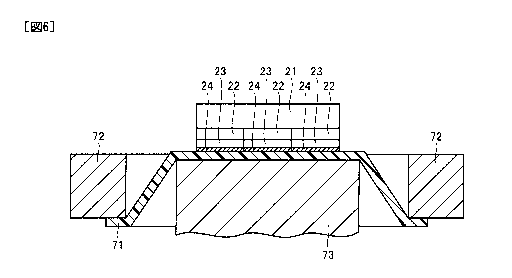
Next, as a step (S50), a supporting layer removing step is performed. In this
step (S50), supporting layer 21 is removed while the plurality of SiC
substrates 22 of
second intermediate wafer 12 are supported by adhesive tape 71 with SiC
substrates 22
being arranged side by side when viewed in a planar view. Specifically,
referring to
Fig. 6, the main surface of adhesive tape 71 opposite to its side holding
second
intermediate wafer 12 is pressed by a pressing member 73 in the axial
direction of ring
frame 72. Accordingly, adhesive tape 71 is elastically deformed, whereby at
least
supporting layer 21 of second intermediate wafer 12 held by adhesive tape 71
is
deviated from the location surrounded by the inner circumference surface of
ring frame
72. Then, supporting layer 21 is pressed against a grinding surface of a
grinding
device such as a grinder (not shown), thereby grinding supporting layer 21.
Accordingly, supporting layer 21 is removed as shown in Fig. 7. In doing so, a
portion
of each of SiC substrates 22 may be removed by the grinding. Further, after
the
removal of supporting layer 21, a total value of the thickness of each SiC
substrate and
the thickness of active layer 23 can be 150 gm or smaller. In this way,
semiconductor
devices to be fabricated will have reduced on-resistance.
Next, as a step (S60), a tape replacing step is performed. In this step,
adhesive
tape 71 is replaced after completing step (S50) by finishing the pressing of
adhesive
tape 71 by pressing member 73. This step (S60) is not an essential step in the
method
for manufacturing the semiconductor device in the present invention, but a
defect
resulting from damage on adhesive tape 71 can be avoided in advance by
replacing
adhesive tape 71, which might be damaged in step (S50) as a result of the
elastic
-13-
111142: 911342
CA 02781665 2012-05-23
deformation or the like.
Next, referring to Fig. 1, a backside electrode forming step is performed. In
this step, a backside electrode is formed on the main surfaces of SiC
substrates 22
exposed by the removal of the supporting layer in step (S50). This backside
electrode
forming step includes a metal layer forming step performed as a step (S70),
and a tape
replacing step performed as a step (S80), and an annealing step performed as a
step
(S90). In step (S70), referring to Fig. 8, a metal layer made of a metal such
as nickel
is formed on the main surfaces of SiC substrates 22 opposite to the side on
which active
layer 23 is formed. This metal layer can be formed using sputtering, for
example.
On this occasion, adhesive tape 71, ring frame 72, and the wafer may be cooled
using a
cooling structure (not shown) as required.
Next, in step (S80), adhesive tape 71 is replaced after completion of step
(S70).
This step (S80) is not an essential step in the method for manufacturing the
semiconductor device in the present invention, but a defect resulting from
damage or
the like on adhesive tape 71 can be avoided in advance by replacing adhesive
tape 71,
which might be damaged in the processes up to step (S70), or by replacing it
with
another adhesive tape 71 suitable for a below-described step (S90).
Next, in step (S90), the metal layer formed in step (S70) is heated.
Specifically, referring to Fig. 8, when the metal layer made of, for example,
nickel is
formed in step (S70), regions of the metal layer in contact with at least SiC
substrates
22 are silicided by the heating in step (S90), thereby obtaining a backside
electrode 25
making ohmic contact with SiC substrates 22.
Next, a reversing step is performed as a step (S 100). In this step (S 100),
referring to Fig. 8 and Fig. 9, an adhesive tape is adhered to the side on
which backside
electrode 25 is formed, and the adhesive tape at the front-side electrode 24
side is
removed. Accordingly, the plurality of SiC substrates 22 are supported by
adhesive
tape 71 with SiC substrates 22 being arranged side by side when viewed in a
planar
view. Accordingly, as shown in Fig. 9, the wafer is held by adhesive tape 71
with the
-14-
111142: 911342
CA 02781665 2012-05-23
wafer being reversed from the state shown in step (S90). As a result, the
front-side
surface of the wafer can be observed, whereby the next step (S 110) can be
readily
performed.
Next, as step (S 110), a dicing step is performed. In this step (S 110),
referring
to Fig. 9, SiC substrates 22 supported by adhesive tape 71 at the backside
electrode 25
side are cut (diced) in the thickness direction thereof with SiC substrates 22
being
arranged side by side when viewed in a planar view. In this way, a plurality
of
semiconductor devices 1 are obtained. It should be noted that this cutting may
be
performed by means of laser dicing or scribing.
Here, in the method for manufacturing semiconductor device 1 in the present
embodiment, combined wafer 10 is prepared which has the plurality of SiC
substrates
22 each made of silicon carbide single-crystal, arranged side by side when
viewed in a
planar view, and each having one main surface connected to supporting layer 21
(see
Fig. 2). Such a combined wafer 10 can be handled as a silicon carbide
substrate
having excellent crystallinity and having a large diameter. Use of combined
wafer 10
allows for efficient manufacturing of semiconductor devices 1.
Further, in the method for manufacturing semiconductor device 1 in the present
embodiment, supporting layer 21 is removed while second intermediate wafer 12
is
supported using adhesive tape 71. Further, the plurality of SiC substrates 22
are kept
on being supported by adhesive tape 71 with SiC substrates 22 being arranged
side by
side when viewed in a planar view until SiC substrates 22 are cut to obtain
the plurality
of semiconductor devices 1 in the subsequent step (S 110). As a result, the
plurality of
SiC substrates 22 are avoided from being separated from one another, thereby
allowing
for efficient manufacturing of semiconductor devices 1.
Further, the wafer (SiC substrates 22) has been thinned due to the removal of
supporting layer 21 to thereby have decreased hardness. However, in the above-
described manufacturing method, the wafer is reinforced by adhesive tape 71
while
being held, thereby restraining damage on the wafer during the process.
Further, the
-15-
CA 02781665 2012-05-23 111142:911342
wafer having been thinned due to the removal of supporting layer 21 and thus
adhered
to adhesive tape 71 held by ring frame 72 is transferred between devices for
performing
the above-described steps. Accordingly, the wafer can be smoothly transferred
between the devices.
Thus, in the method for manufacturing the semiconductor device in the present
embodiment, the process is simple and manufacturing efficiency is excellent.
Hence,
the manufacturing method is suitable for mass production of semiconductor
devices.
Here, the replacement of adhesive tape 71 in each of step (S60) and step (S80)
can be implemented as follows. First, the plurality of SiC substrates 22
arranged side
by side when viewed in a planar view are held by an adsorbing member.
Thereafter,
the adhesive tape is detached and then a new adhesive tape is adhered.
Thereafter, the
adsorption by the adsorbing member is terminated.
In addition, the adhering and removal of adhesive tape 71 in each of steps
(S60),
(S80), (S 100), and the like may be automated.
Further, in the above-described step (S90), front-side electrode 24 may have a
temperature maintained at 180 C or smaller. Hence, the adhesive tape does not
need
to have a high heat resistance, thereby providing a wider range of choices for
a material
for the adhesive tape. Thus, a general resin tape can be employed as the above-
described adhesive tape, for example.
Further, in step (S90), it is preferable to locally heat the metal layer. This
achieves suppressed damage on a wire formed in step (S30), adhesive tape 71,
and the
like. This local heating may be attained by laser irradiation for the metal
layer. In
this way, the local heating can be readily done.
Further, the above-described laser preferably has a wavelength of 355 nm. In
this way, even in the case where the metal layer has a defect portion such as
a pinhole,
the metal layer can be appropriately heated while suppressing damage on front-
side
electrodes 24, a surrounding device, and the like.
Further, as the laser, a pulse laser having a pulse width of not less than 10
nsec
-16-
111142: 911342
CA 02781665 2012-05-23
and not more than 50 nsec can be employed. Further, the laser can be adapted
to have
an energy density of not less than 0.5 J/cm2 and not more than 2 J/cm2. If the
energy
density is less than 0.5 J/cm2, the energy will be insufficient to result in
insufficient
heating. Accordingly, sufficient ohmic contact may not be obtained. On the
other
hand, if the energy density is more than 2 J/cm2, surface ablation may take
place to
result in scattering of an electrode, increased resistance, and the like,
disadvantageously.
Further, for the adhesive tape of the present embodiment, there may be used an
adhesive tape (UV tape) having adhesive force to be reduced when irradiated
with
ultraviolet rays, or an adhesive tape having adhesive force to be reduced when
being
heated. By thus employing the adhesive tape having its adhesive force which
can be
reduced as required, the above-described manufacturing process can be
performed
smoothly.
Further, in step (S 10), combined wafer 10 may be prepared in which the main
surface of each SiC substrate 22 opposite to supporting layer 21 may have an
off angle
of not less than 50 and not more than 65 relative to the {00011 plane. In
this way,
for example, when a channel region is formed in the vicinity of an interface
between
active layer 23 formed in step (S20) and the gate oxide film formed on active
layer 23,
formation of interface states are suppressed in the vicinity of the interface.
Accordingly, semiconductor device 1 having reduced on-resistance can be
manufactured.
Further, in step (S 10), combined wafer 10 may be prepared in which the main
surface of each SiC substrate 22 opposite to supporting layer 21 has an off
orientation
forming an angle of 5 or smaller relative to the <01-10> direction. In this
way, an
epitaxial growth layer or the like can be formed readily on SiC substrate 22.
Further,
the main surface of SiC substrate 22 opposite to supporting layer 21 may have
an off
angle of not less than -3 and not more than 5 relative to the {0-33-8} plane
in the
<01-10> direction. In this way, there can be obtained semiconductor device 1
in
which the formation of interface states can be further suppressed to achieve
further
-17-
111142: 911342
CA 02781665 2012-05-23
reduced on-resistance. Further, the main surface of SiC substrate 22 opposite
to
supporting layer 21 is adapted to correspond to a plane of the carbon plane
side,
whereby semiconductor device 1 having further reduced on-resistance can be
manufactured.
Meanwhile, in step (S 10), there may be prepared a combined wafer in which the
main surface of each SiC substrate 22 opposite to supporting layer 21 has an
off
orientation forming an angle of 5 or smaller relative to the <-2110>
direction. Also
in this case, an epitaxial growth layer or the like can be formed readily on
SiC substrate
22.
It should be noted that the semiconductor device that can be manufactured in
accordance with the method for manufacturing the semiconductor device in the
present
invention is not particularly limited as long as it is a semiconductor device
having a
front-side electrode and a backside electrode. For example, a MOSFET, an IGBT
(Insulated Gate Bipolar Transistor), a JFET (Junction Field Effect
Transistor), a diode,
or the like can be manufactured in accordance with the manufacturing method in
the
present invention.
The embodiments disclosed herein are illustrative and non-restrictive in any
respect. The scope of the present invention is defined by the terms of the
claims,
rather than the embodiments described above, and is intended to include any
modifications within the scope and meaning equivalent to the terms of the
claims.
INDUSTRIAL APPLICABILITY
The method for manufacturing the semiconductor device in the present
invention is advantageously applicable to a method for manufacturing a
semiconductor
device using a silicon carbide substrate.
REFERENCE SIGNS LIST
1: semiconductor device; 10: combined wafer; 11: first intermediate wafer; 12:
second intermediate wafer; 21: supporting layer; 22: SiC substrate; 23: active
layer; 24:
front-side electrode; 25: backside electrode; 71: adhesive tape; 72: ring
frame; 73:
-18-
111142: 911342
CA 02781665 2012-05-23
pressing member.
-19-