Note: Descriptions are shown in the official language in which they were submitted.
CA 02781795 2012-06-26
TRANSMITTER INCLUDING CALIBRATION OF AN
IN-PHASE/QUADRATURE (I/Q) MODULATOR AND ASSOCIATED
METHODS
Field of the Invention
[0001] The present invention relates to the field of wireless communications,
and
more particularly, to calibration of an analog in-phase/quadrature (I/Q)
modulator for
gain, phase and DC offset imperfections.
Background of the Invention
[0002] Modulators are used within transmitters to modulate an input signal
with
a radio frequency (RF) signal. The modulated input signal may include voice
and
data, for example. One type of modulator is an in-phase/quadrature (I/Q)
modulator.
An I/Q modulator receives an in-phase (I) signal and a quadrature (Q) signal
and
modulates the I and Q signals with an RF signal.
[0003] An I/Q modulator is also known as a vector modulator, and is commonly
used to support different types of modulation in a single package. Many
transmitters
rely on an analog implementation of an I/Q modulator. An analog I/Q modulator
typically requires calibration whereas a digitally implemented I/Q modulator
typically
does not.
[0004] More particularly, an analog I/Q modulator suffers from imperfect
carrier
rejection 10 caused by DC offsets between signal paths, as illustrated in FIG.
1 for a
single tone modulation. An analog I/Q modulator also suffers from imperfect
sideband rejection 12 caused by gain and phase imbalance, as illustrated in
FIG. 2 for
a single tone modulation. These imperfections lead to gain, phase and DC
offset
imperfections which may degrade transmitter performance. Degraded transmitter
performance includes reduced adjacent power rejection, FM distortion and AM
ripple.
[0005] Imperfect carrier rejection and imperfect sideband rejection can be
compensated manually or electronically. Single tone approaches may require
feedback paths and analog-to-digital converters with sufficient speed to
measure the
feedback envelopes.
-1-
CA 02781795 2012-06-26
[0006] One calibration approach is disclosed in an article titled "Adaptive
Compensation for Imbalance and Offset Losses in Direct Conversion
Transceivers"
by Cavers, IEEE Transactions on Vehicular Technology, Vol. 42, No. 4, November
1993, pp. 581-588. In a calibration phase, a continuous calibration tone is
provided to
the I/Q modulator for modulation, and an envelope detector receives the
continuous
modulated calibration tone. Sample points from the continuous modulated
calibration
tone are then converted from analog-to-digital for input to a calibration
algorithm. A
drawback of this approach is that the analog-to-digital converter as well as
the
feedback data needs to be fast enough to read the envelope data output from
the
modulator to measure the tone frequencies. This requirement results in
increased cost
and power consumption. Not only is proper timing alignment needed between the
generated continuous calibration tone and the feedback envelope, but multiple
analog-
to-digital converters may be needed, which further results in increased cost
and power
consumption.
[0007] Another approach for calibrating an I/Q modulator in a transmitter is
disclosed in U.S. Patent No. 6,798,844. The transmitter includes an I/Q
modulator
and a compensator for correcting the phase and amplitude imbalance caused by
the
I/Q modulator. A feedback path samples the I/Q-modulated test signal to be
transmitted, an analog-to-digital converter converts the signal samples taken
from the
test signal, a demodulator demodulates the signal samples digitally into in-
phase and
quadrature feedback signals, and an adapter determines the phase and amplitude
imbalance caused by the I/Q modulator on the basis of the in-phase and
quadrature
feedback signals. The adapter then determines and provides to the compensator
the
correction parameters of phase and amplitude on the basis of the determined
phase
and amplitude imbalance.
[0008] Yet another approach to calibrate a modulator is disclosed in U.S.
Patent
No. 7,092,454. Calibration parameters are provided to a calibration network so
that
the modulator receives a pair of predetermined sinusoidal in-phase and
quadrature
signals and outputs a distorted modulated signal. A processor then processes
spectral
-2-
CA 02781795 2012-06-26
parameters at first and second harmonics of a detected envelope signal of the
distorted
modulated signal to generate the calibration parameters for the calibration
network.
[00091 A drawback of the approaches disclosed in the `844 and `454 patents is
that they also require proper timing alignment between the generated
calibration
parameters and the feedback envelope, as well as requiring the calibration to
be
performed at sufficient speed to measure the feedback envelopes.
Summary of the Invention
[00101 In view of the foregoing background, it is therefore an object of the
present
invention to simplify calibration of an I/Q modulator within a transmitter.
[00111 This and other objects, features, and advantages in accordance with the
present invention are provided by a transmitter comprising an input, a
modulator, a
calibration memory configured to store a plurality of discrete calibration
test points,
and a compensator coupled between the input and the modulator and configured
to
cooperate with the calibration memory to cause the modulator to generate a
respective
calibration carrier signal for each of the discrete calibration test points
during a
calibration phase.
[00121 A detector may be coupled to an output of the modulator and configured
to
determine respective calibration values of the calibration carrier signals
during the
calibration phase. A compensator calculator may be coupled to an output of the
detector and configured to generate compensation values for the compensator
for use
during an operation phase and based on the calibration values of the
calibration carrier
signals.
100131 The modulator may be an analog I/Q modulator. An advantage of using
stored discrete calibration test points for the analog I/Q modulator is that a
continuous
calibration tone is not required. This in turn allows the calibration phase to
be
performed at a slower rate of speed since proper timing alignment between the
detector and the discrete test points is not required. In addition, the
discrete
calibration test points may be randomly applied to the compensator during the
calibration phase.
-3-
CA 02781795 2012-06-26
[00141 The transmitter may further comprise an analog-to-digital converter
between the detector and the compensator calculator. Another advantage of the
calibration phase being able to be performed at a slower rate of speed is that
a low
performance analog-to-digital converter may be used. A low performance analog-
to-
digital converter is lower in cost and power consumption as compared to faster
performing analog-to-digital converters needed for keeping up with continuous
calibration test tones.
[00151 An interface between the analog-to-digital converter and the
compensator
calculator may be a serial interface. Another advantage of the calibration
phase being
able to be performed at a slower rate of speed is that a low throughput data
bus may
be used to provide the respective digitized calibration values of the
calibration carrier
signals to the compensator calculator. A serial interface thus reduces the
interface
burden between the analog-to-digital converter and the compensator calculator.
[00161 The compensator calculator may be configured to generate the
compensation values via a series of iterative steps. The discrete calibration
test points
stored in the calibration memory may be used in a first iterative step and the
compensation values generated in response thereto may then be used as the
discrete
calibration test points in a next iterative step, with the iteration repeating
a set number
of times. Alternatively, the iteration may repeat until changes in the
compensation
values become less than a set value.
[00171 The transmitter may further comprise a multiplexer between the input
and
the compensator, with the multiplexer being configured to be responsive to a
control
signal for providing the plurality of discrete calibration test points to the
compensator
during the calibration phase. The multiplexer may also provide in-phase and
quadrature data from the input to the compensator for compensation during the
operation phase. The detector may comprise an envelope detector, an RMS
detector
or a log detector, for example.
100181 Another aspect of the invention is directed to a method for calibrating
a
modulator within a transmitter as described above. The method may comprise
storing
discrete calibration test points in a calibration memory. A compensator is
coupled
-4-
CA 02781795 2012-06-26
between an input and the modulator is operated to cooperate with the
calibration
memory to cause the modulator to generate a respective calibration carrier
signal for
each of the discrete calibration test points during a calibration phase. The
method
may further comprise operating a detector coupled to an output of the
modulator to
determine respective calibration values of the calibration carrier signals
during the
calibration phase. A compensator calculator coupled to an output of the
detector may
be operated to generate compensation values for the compensator for use during
an
operation phase and based on the calibration values of the calibration carrier
signals.
Brief Description of the Drawings
[0019] FIG. 1 is a graph illustrating the effects of DC offset for a single
tone
modulation in accordance with the prior art.
[0020] FIG. 2 is a graph illustrating the effects of gain and phase imbalance
for a
single tone modulation in accordance with the prior art.
[0021] FIG. 3 is a block diagram of a transmitter that includes calibration
circuitry
for calibrating an I/Q modulator within the transmitter in accordance with the
present
invention.
[0022] FIG. 4 is a unit circle plot of an I/Q constellation illustrating the
discrete
calibration test points stored in the calibration memory in accordance with
the present
invention.
[0023] FIG. 5 is a QAM plot of an I/Q constellation illustrating the discrete
calibration test points stored in the calibration memory in accordance with
the present
invention.
[0024] FIG. 6 is a block diagram illustrating a method for calibrating an I/Q
modulator within a transmitter in accordance with the present invention.
Detailed Description of the Preferred Embodiments
[0025] The present invention will now be described more fully hereinafter with
reference to the accompanying drawings, in which preferred embodiments of the
invention are shown. This invention may, however, be embodied in many
different
-5-
CA 02781795 2012-06-26
forms and should not be construed as limited to the embodiments set forth
herein.
Rather, these embodiments are provided so that this disclosure will be
thorough and
complete, and will fully convey the scope of the invention to those skilled in
the art.
Like numbers refer to like elements throughout, and prime notation is used to
indicate
similar elements in alternative embodiments.
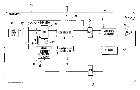
[00261 Referring now to FIG. 3, a transmitter 20 including calibration
circuitry 30
for calibrating an I/Q modulator 40 within the transmitter will now be
described. The
I/Q modulator 50 is illustratively an analog I/Q modulator. The calibration
circuitry
30 includes a calibration memory 32 for storing discrete calibration test
points, a
compensator 34 and a compensator calculator 36.
[00271 The compensator 34 is coupled between an input 60 and the I/Q modulator
50, and cooperates with the calibration memory 32 to cause the I/Q modulator
to
generate a respective calibration carrier signal for each of the discrete
calibration test
points during a calibration phase.
[00281 A detector 70 is coupled to an output of the I/Q modulator 40 and is
configured to determine respective calibration values of the calibration
carrier signals
during the calibration phase. The detector 70 may be configured as an envelope
detector to determine calibration amplitudes of the calibration carrier
signals.
Alternatively, the detector 70 may be configured as a log detector or an RMS
detector.
[00291 The compensator calculator 36 is coupled to an output of the detector
70
and is configured to generate compensation values for the compensator 34 for
use
during an operation phase and based on the calibration values of the
calibration carrier
signals.
[00301 The illustrated calibration memory 32 is included as part of a driver
38.
Alternatively, the calibration memory 32 and driver 38 may be separate from
one
another. The driver 38 controls a multiplexer 80 positioned between the input
60 and
the compensator 34. During the calibration phase, the driver 38 controls the
multiplexer 80 via control line 82 so that the discrete calibration test
points are input
into the multiplexer via test point lines 84.
-6-
CA 02781795 2012-06-26
[0031] Once the I/Q modulator 50 has been calibrated, then the driver 38
controls
the multiplexer 80 via control line 82 so that an I/Q data generator 90
provides I/Q
data to be compensated prior to modulation by the I/Q modulator during the
operation
phase. The multiplexer 80 thus places the transmitter 20 in the calibration
phase or
the operation phase. During the operation phase, the modulated I/Q data is
passed to
an amplifier 92 and antenna 94 prior to be transmitted over the airwaves.
[0032] For illustration purposes, 8 discrete calibration test points are
stored in the
calibration memory 32, as provided in TABLE 1. A plot or graph of an I/Q
constellation 42 illustrating the 8 discrete calibration test points ml-m8
with respect
to output of the detector 70 is provided in FIG. 4. As illustrated, the
calibration test
points ml-m8 are evenly spaced around the I/Q constellation 42. As readily
appreciated by those skilled in the art, a different number of discrete
calibration test
points maybe stored. Alternatively, the calibration test points ml-m16 may be
part of
a 16-QAM constellation, as illustrated in FIG. 5. One of the important
advantages is
to avoid the need for a tone generator to generate a calibration test tone
that would
instead have to be used during the calibration test phase.
[0033] Since there is variation from modulator to modulator and across the RF
frequency band, the compensation values as determined by the compensator
calculator 36 for gain, phase and DC offsets are determined during operation
of the
transmitter 20. A digital-to-analog converter 96 converts the input to the I/Q
modulator 50 to analog values, and an analog-to-digital converter 98 converts
the
output of the I/Q modulator 50 to digital values. The calibration circuitry 30
may be
operated prior to keying the transmitter 20, for example. Since the
calibration
circuitry 30 can be operated at a relatively low rate of speed since discrete
calibration
test points are being used, the transmitter 20 may be perform other functions
during
the calibration process.
[0034] The compensation values are iteratively computed by the compensator
calculator 36. The calibration process is initialized with the 8 discrete
calibration test
points. The calibration process is based on sampling the output of the
detector 70 for
eight different settings of the discrete calibration test points to the I/Q
modulator 50.
-7-
CA 02781795 2012-06-26
The eight discrete calibration test points ml-m8 are evenly spaced around the
IQ
constellation 42, as illustrated in FIG. 4, and are represented as the values.
TABLE 1
Relative IQ Test Points
Test Point I value Q value Detector
Sample
1 1 0 MI
2 .707 .707 m2
3 0 1 m3
4 -.707 .707 m4
-1 0 m5
6 -.707 -.707 m6
7 0 -I m7
8 .707 -.707 m8
[00351 The calibration test points are relative values and do not represent
the
actual output voltages from the digital-to-analog converter 96. The actual
output
values are scaled and offset by a DC value in accordance with the operation of
the I/Q
modulator 50.
[00361 Prior to initialization of the calibration process, the compensation
values
are set to zero within the compensator calculator 36.
Cgarn = 0
Cphase = 0
CI _OJ)set = 0
CQOJ,jrel - 0
[00371 For each of the discrete calibration test points as provided in TABLE
1, the
output of the detector 70 is read and saved. After all eight discrete
calibration test
-8-
CA 02781795 2012-06-26
points have been tested, four error estimates are computed by the compensator
calculator 36 as shown below.
m,-m3+m5-m7
gain 2
m2 - m4 + m6 -M 8
P phase 2
- m, - m5 +.707 * (m2 - m4 - m6 +M8)
P/ Uffse, - 4
m3 - m7 + .707 * (m2 + m4 - m6 - m8 )
PQOffse~ 4
[00381 Generally speaking, the above error estimates may be computed as
follows
for any set of N calibration points. The coefficients cg j,Cp j,Cioffj,Cgoffj
are sets of pre-
computed coefficients that are a function of the set of N discrete calibration
points.
N
gain = Y. mj * Cgj
j=1
N
phase = I mj * CPd
j=1
N
i-offset = Y, mj * CioffJ
j=1
N
9-offset = Y. mj * C9off j
j=1
100391 The compensation values are updated by subtracting the error estimates
computed above from the current compensation values.
-9-
CA 02781795 2012-06-26
Cgain Cgain - Kloop ' Pgain
Cphase = C phase - Kloop ' luphase
CI -Offset C1.Ofjcei - Kloop ' PI -Offset
CQOffcei CQ_OfJsei - Kloop Offsei
[0040] Where Cgain is the gain compensation value, Cphase is the phase
compensation value, C1 Offset is the baseband in-phase DC offset compensation
value
and CQ_Offset is the baseband quadrature DC offset compensation value. The
values mx
are the measurements made for each of the respective discrete calibration test
points
from TABLE 1.
100411 Each of these values are to be scaled by a gain value, Kloop that
represents
the loop gain of a closed loop system. This scaling value depends on the
particular
components of the calibration circuitry and analog I/Q modulator, as readily
understood by those skilled in the art.
[0042] The I and Q values are adjusted by the compensator 34 based on the
compensation calculator 36 modifying the value (e.g., amplitude) of each path,
adjusting the phase of each path by cross coupling between the paths and then
finally
a constant is added. The adjustments or updated compensation values to the I
and Q
values are shown in the equations below.
a=1+Cgain
2
1- gain
2
C phase
I comp = a - Ibb + 2 Qbb + CI -Offset
Cphase
comp = N - Qbb + 2 - Ibb + CQ Offset
-10-
CA 02781795 2012-06-26
[0043] Ibb and Qbb are the uncompensated baseband I and Q values and Icomp and
Qcomp are the compensated I and Q values that are written to the digital-to-
analog
converter 96 driving the analog I/Q modulator 50. The new compensated I and Q
values are computed and used as the test points in the next iteration.
Measurements
are made again and the compensation values are re-computed. The calibration
process iterates for either a set number of times or until the changes in the
compensation values become smaller than a set value.
[0044] As noted above, the compensator calculator 36 generates the
compensation
values via a series of iterative steps. The discrete calibration test points
stored in the
calibration memory 32 are thus used in a first iterative step and the
compensation
values generated in response thereto are then be used as the discrete
calibration test
points in a next iterative step.
[0045] Another aspect of the invention is directed to a method for calibrating
a
modulator 50 within a transmitter 20 as described above. Referring now to the
flowchart 200 in FIG. 5, from the start (Block 202), the method comprises
storing
discrete calibration test points in a calibration memory 32 at Block 204. A
compensator 34 is coupled between an input 60 and the modulator 50 is operated
at
Block 206 to cooperate with the calibration memory 32 to cause the modulator
to
generate a respective calibration carrier signal for each of the discrete
calibration test
points during a calibration phase.
[0046] The method further comprises operating a detector 70 coupled to an
output
of the modulator 50 to determine respective calibration values (e.g.,
amplitudes) of
the calibration carrier signals during the calibration phase at Block 208. A
compensator calculator 36 coupled to an output of the detector 70 is operated
at Block
210 to generate compensation values for the compensator for use during an
operation
phase and based on the calibration values of the calibration carrier signals.
[0047] As noted above, the compensator calculator 36
is configured to generate the compensation values via a series of iterative
steps. A
determination is made at decision Block 212 based on the generated
compensation
values from Block 210. If the generated compensation values are less than a
-11-
CA 02781795 2012-06-26
predetermined value, then the process loops to Block 214 so that the
compensator 34
generates a respective carrier signal for each of the compensation values that
are now
used as discrete calibration test points.
[0048] In other words, the discrete calibration test points stored in the
calibration
memory 32 are used in a first iteration, and the compensation values generated
in
response thereto are used as the discrete calibration test points in a next
iteration. The
iteration repeats until changes in the compensation values become less than a
set
value. Alternative, the iteration may repeat a set number of times. The method
ends
at Block 216.
-12-