Note: Descriptions are shown in the official language in which they were submitted.
CA 2781841 2017-04-25
OPTICAL DEVICE HAVING MODULATOR EMPLOYING HORIZONTAL
ELECTRICAL FIELD
[0001] This application claims priority from U.S. Patent Application serial
number 12/653,547, filed on December 15, 2009, entitled "Optical Device Having
Modulator Employing Horizontal Electrical Field", which issued to U.S. Patent
No.
8,346,028 B2 on January 1, 2013.
[0002]
FIELD
[0003] The present invention relates to optical devices and more
particularly to
devices having optical modulators.
BACKGROUND
[0004] The use of optical and/or optoelectronic devices is increasing in
communications
applications. These devices can include modulators for phase and/or intensity
modulating
light signals. These modulators have been able to achieve adequate speeds when
the
waveguides have a cross-section with sub-micron dimensions. However, many
communications applications employ larger waveguides. When these modulators
are used
with larger waveguides, they generally lose speed as a result of the need for
carriers to
travel through the larger dimensions of the waveguide.
[0005] For the above reasons, there is a need for modulators that are
suitable for
use with larger waveguides.
SUMMARY
[0006] An optical device includes a waveguide on a base. The device also
includes a modulator on the base. The modulator includes an electro-absorption
medium
configured to receive a light signal from the waveguide. The modulator also
includes
field sources for generating an electrical field in the electro-absorption
medium. The
electro-absorption medium is a medium in which the Franz-Keldysh effect occurs
in
response to the formation of the electrical field in the electro-absorption
medium. The
field sources are configured so the electrical field is substantially parallel
to the base.
[0007] One embodiment of the device includes an optical waveguide on a
base.
The waveguide is configured to guide a light signal through a light-
transmitting medium.
1
CA 2781841 2017-04-25
A modulator is also positioned on the base. The modulator including a ridge
extending
from slab regions. The slab regions are positioned on opposing sides of the
ridge. An
electro-absorption medium is positioned to receive at least a portion of the
light signal
from the light-transmitting medium included in the waveguide. The electro-
absorption
medium is included in the ridge and also in the slab regions. The electro-
absorption
medium includes doped regions positioned such that application of a bias
across the
doped regions forms an electrical field in the electro-absorption medium
included in the
ridge.
[0008] Another embodiment of the optical device includes an optical
waveguide
on a base. The waveguide is configured to guide a light signal through a light-
transmitting medium. A modulator is positioned on the base and includes
electro-
absorption medium configured to receive the light signal from the waveguide.
The
electro-absorption medium has lateral sides that are each positioned between a
top side
and a bottom side with the bottom side being between the base and the top
side. The
light-transmitting medium and the electro-absorption medium are different
materials. The
modulator also includes field sources configured to serve as sources of an
electrical field
in the electro-absorption medium. The field sources each contact one of the
lateral sides
and the lateral sides that are contacted by the field sources are on opposing
sides of the
electro-absorption medium.
[0008a] Accordingly, in one of its aspects, the present invention provides
an
optical device, comprising: a waveguide on a base, the waveguide configured to
guide a
light signal through a light-transmitting medium; and a modulator positioned
on the base,
the modulator including an electro-absorption medium having lateral sides that
each
extends between a top side and a bottom side, the bottom side being between
the base and
the top side, the electro-absorption medium configured to receive at least a
portion of the
light signal from the light-transmitting medium in the waveguide, the light-
transmitting
medium and the electro-absorption medium being different materials, doped
regions of
the electro-absorption medium configured to serve as sources of an electrical
field in the
electro-absorption medium, the electro-absorption medium being a medium in
which the
Franz-Keldysh effect occurs in response to the formation of the electrical
field in the
electro-absorption medium, the doped regions each contacting one of the
lateral sides and
2
CA 2781841 2017-04-25
the lateral sides that are contacted by the doped regions being on opposing
sides of the
electro-absorption medium.
[0008b] Further aspects of the invention will become apparent upon reading
the
following detailed description and drawings, which illustrate the invention
and preferred
embodiments of the invention.
BRIEF DESCRIPTION OF THE FIGURES
[0009] Figure lA through Figure 1J illustrate an optical device having an
optical
modulator configured. The modulator includes field sources that are configured
to
generate a substantially horizontal electrical field in an electro-absorption
medium. The
device illustrated in Figure IA through Figure 1J employs doped regions of the
electro-
absorption medium as the field sources. Figure lA is a perspective view of the
device.
[0010] Figure 1B is a topview of the portion of the optical device shown in
Figure
1A that includes the optical modulator.
[0011] Figure 1C is a cross-section of the device shown in Figure 1A taken
along
the line labeled C.
[0012] Figure 1D is a cross-section of the optical device shown in Figure
lA
taken along the line labeled D.
[0013] Figure 1E is a cross-section of the optical device shown in Figure
IA
taken along the line labeled E.
[0014] Figure IF is a cross-section of the optical device shown in Figure
1A
taken along the line labeled F.
2a
00 02781841 2012-M24
WO 2011/075157 PCT/US2010/002959
[0015] Figure 1G is a cross-section of the optical device shown in Figure
lA taken
along the line labeled F.
[0016] Figure 1H is a cross-section of the optical device shown in Figure
lA taken
along the line labeled F. The embodiments shown in Figure 1F, Figure 1G, and
Figure 1H
are alternative embodiments.
[0017] Figure 1J is a cross-section of the optical device shown in Figure
1A taken
along the line labeled J. The cross section is through a modulator constructed
on a
waveguide having a structure according to Figure 1F.
[0018] Figure 2A is a cross section of an embodiment of a modulator that
can be
constructed on a waveguide having a structure constructed according to Figure
1H.
[0019] Figure 2B is a cross section of an embodiment of a modulator that
can be
constructed on a waveguide having a structure constructed according to Figure
1G.
[0020] Figure 2C is a cross section of an embodiment of a modulator that
can be
constructed on a waveguide having a structure constructed according to Figure
1F.
[0021] Figure 3 is a topview of the optical device of Figure 1B where the
waveguide
includes horizontal tapers and excludes vertical tapers.
100221 Figure 4 illustrates an optical device having the modulator
incorporated into a
Mach-Zehnder interferometer.
[0023] Figure 5A through Figure 14 illustrate a method of forming an
optical device
having a modulator constructed according to Figure 1A through Figure 1F, and
Figure 1.J.
DESCRIPTION
[0024] The optical device includes a waveguide positioned on a base. A
portion of
the waveguide includes an electro-absorption medium. The waveguide is
configured such
that light signals guided through the waveguide are received in the electro-
absorption
medium. The device includes field sources in contact with the electro-
absorption medium.
During operation of the modulator, an electrical field can be applied to the
field sources to
form an electrical field in the electro-absorption medium. The electro-
absorption medium
can be a medium in which the Franz-Keldysh effect occurs. As a result,
application of the
=
electrical field to the electro-absorption medium causes an increase in the
absorption of light
by the electro-absorption medium. The electrical field can be tuned so as to
modulate the
level of absorption of the light signals. Further, the electrical field needed
to take advantage
of the Franz-Keldysh effect generally does not involve excitation of carriers
by the electric
field. Since the formation and tuning of the electrical field is not dependent
on the movement
3
00 02781841 2012-M24
WO 2011/075157 PCT/US2010/002959
of carriers, the modulator can provide high speed modulation. For instance, in
some instance,
the modulator can provide modulation on the order of 40GHz.
[0025] Additionally, the field sources can be arranged such that the
resulting
electrical field is substantially parallel to the base or is substantially
horizontal. For instance,
the field sources can be positioned on the lateral sides of the electro-
absorption medium.
Since the electrical field can be substantially parallel to the base,
narrowing the width of the
electro-absorption medium increases the speed of the modulator. As a result,
the width of the
waveguide can be horizontally tapered in order to increase the modulation
speed. Further,
this increase in modulation speed can be achieved without reducing the height
of the
electro-absorption medium. As a result, the increased speed can be achieved
without the use
of vertical tapers that are often associated with optical loss and fabrication
challenges. Since
the modulator speed can be increased by using a horizontal taper but without a
vertical taper,
the modulator can provide acceptable modulation speeds for waveguides having
larger
dimensions.
[0026] Figure 1A through Figure 1J illustrate an optical device having a
waveguide
that includes a modulator. Figure 1A is a perspective view of the device.
Figure 1B is a
topview of the portion of the optical device shown in Figure lA that includes
an optical
modulator. Figure 1C is a cross-section of the device shown in Figure lA taken
along the
line labeled C. Figure 1D is a cross-section of the optical device shown in
Figure IA taken
along the line labeled D. Figure 1E is a cross-section of the optical device
shown in Figure
IA taken along the line labeled E. Figure 1F is a cross-section of the optical
device shown in
Figure lA taken along the line labeled F. Figure 1G is a cross-section of the
optical device
shown in Figure 1A taken along the line labeled F. Figure 1H is a cross-
section of the optical
device shown in Figure IA taken along the line labeled F. The embodiments
shown in Figure
1F, Figure 1G, and Figure 1H are alternative embodiments. Figure 1J is a cross-
section of
the optical device shown in Figure 1A taken along the line labeled J.
[0027] The device is within the class of optical devices known as planar
optical
devices. These devices typically include one or more waveguides immobilized
relative to a
substrate or a base. The direction of propagation of light signals along the
waveguides is
generally parallel to a plane of the device. Examples of the plane of the
device include the
top side of the base, the bottom side of the base, the top side of the
substrate, and/or the
bottom side of the substrate.
[0028] The illustrated device includes lateral sides 10 (or edges)
extending from a top
side 12 to a bottom side 14. The propagation direction of light signals along
the length of the
4
CA 02781841 2012-M24
WO 2011/075157 PCT/US2010/002959
waveguides on a planar optical device generally extends through the lateral
sides 10 of the
device. The top side 12 and the bottom side 14 of the device are non-lateral
sides.
[0029] The device includes one or more waveguides 16 that carry light
signals to
and/or from optical components 17. Examples of optical components 17 that can
be included
on the device include, but are not limited to, one or more components selected
from a group
consisting of facets through which light signals can enter and/or exit a
waveguide, entry/exit
ports through which light signals can enter and/or exit a waveguide from above
or below the
device, multiplexers for combining multiple light signals onto a single
waveguide,
demultiplexers for separating multiple light signals such that different light
signals are
received on different waveguides, optical couplers, optical switches, lasers
that act a source
of a light signal, amplifiers for amplifying the intensity of a light signal,
attenuators for
attenuating the intensity of a light signal, modulators for modulating a
signal onto a light
signal, modulators that convert an light signal to an electrical signal, and
vias that provide an
optical pathway for a light signal traveling through the device from the
bottom side 14 of the
device to the top side 12 of the device. Additionally, the device can
optionally, include
electrical components. For instance, the device can include electrical
connections for
applying a potential or current to a waveguide and/or for controlling other
components on the
optical device.
[0030] A portion of the waveguide includes a first structure where a
portion of the
waveguide 16 is defined in a light-transmitting medium 18 positioned on a base
20. For
instance, a portion of the waveguide 16 is partially defined by a ridge 22
extending upward
from a slab region of the light-transmitting medium as shown in Figure 1C. In
some
instances, the top of the slab region is defined by the bottom of trenches 24
extending
partially into the light-transmitting medium 18 or through the light-
transmitting medium 18.
Suitable light-transmitting media include, but are not limited to, silicon,
polymers, silica, SiN,
GaAs, InP and LiNb03. One or more cladding layers (not shown) are optionally
positioned
on the light-transmitting medium. The one or more cladding layers can serve as
a cladding
for the waveguide 16 and/or for the device. When the light-transmitting medium
18 is silicon,
suitable cladding layers include, but are not limited to, silicon, polymers,
silica, SiN, GaAs,
InP and LiNb03.
[0031] Recesses 25 (Figure 1B) extend into the slab regions such that the
ridge 22 is
positioned between recesses 25. The recesses 25 can extend only part way into
the
light-transmitting medium 18. As is evident from Figure 1D, the recesses 25
can be spaced
apart from the ridge 22. As a result, a portion of the waveguide 16 includes a
second
CA 02781841 2012-M24
WO 2011/075157 PCT/US2010/002959
structure where an upper portion of the waveguide 16 is partially defined by
the ridge 22
extending upward from the slab region and a lower portion of the waveguide is
partially
defined by recesses 25 extending into the slab regions and spaced apart from
the ridge.
[0032] As shown in Figure 1E, the recesses 25 can approach the ridge 22
such that the
sides of the ridge 22 and the sides of the recesses 25 combine into a single
surface 26. As a
result, a portion of a waveguide includes a third structure where the
waveguide is partially
defined by the surface 26.
[0033] As is evident in Figure 1B, a portion of the waveguide includes an
electro-absorption medium 27. The electro-absorption medium 27 is configured
to receive
the light signals from a portion of the waveguide having the third structure
and to guide the
received light signals to another portion of the waveguide having the third
structure.
[0034] The electro-absorption medium 27 extends upward from the bottom of
the
recesses 25. The electro-absorption medium 27 is configured to guide the light
signals. For
instance, as is evident in Figure IF, a portion of a waveguide includes a
fourth structure
where the waveguide is partially defined by the top and lateral sides of the
electro-absorption
medium 27.
[0035] In Figure 1F, the electro-absorption medium 27 is positioned on a
seed portion
34 of the light-transmitting medium 18. The seed portion 34 of the light-
transmitting
medium 18 is positioned on the base 20. In particular, the seed portion 34 of
the
light-transmitting medium 18 contacts the insulator 28. In some instances,
when the light
signal travels from the light-transmitting medium into the electro-absorption
medium 27, a
portion of the light signal enters the seed portion 34 of the light-
transmitting medium 18 and
another portion of the light signal enters the electro-absorption medium 27.
During the
fabrication of the device, the seed portion 34 of the light-transmitting
medium 18 can be used
to grow the electro-absorption medium 27. For instance, when the light-
transmitting medium
18 is silicon and the electro-absorption medium 27 is germanium or germanium-
silicon, the
electro-absorption medium 27 can be grown on the silicon. As a result, the use
of the
light-transmitting medium 18 in both the waveguides 16 and as a seed layer for
growth of the
electro-absorption medium 27 can simplify the process for fabricating the
device.
[0036] Figure 1G is an alternative to the fourth structure illustrated in
Figure IF. In
Figure 1G, the electro-absorption medium 27 is positioned on a seed portion 34
of the
light-transmitting medium 18 without the seed portion 34 of the light-
transmitting medium 18
extending substantially beyond the lateral sides of the electro-absorption
medium 27.
Additionally, the slab regions of the light-transmitting medium 18 are not
present adjacent to
6
00 02781841 2012-M24
WO 2011/075157 PCT/US2010/002959
the ridge of the electro-absorption medium 27. Accordingly, a portion of a
waveguide
includes a fourth structure where the waveguide is partially defined by the
top and lateral
sides of the electro-absorption medium 27. In some instances, when the light
signal travels
from the light-transmitting medium into the electro-absorption medium 27, a
portion of the
light signal enters the seed portion 34 of the light-transmitting medium 18
and another
portion of the light signal enters the electro-absorption medium 27. As
described above, the
electro-absorption medium 27 can be grown on the seed portion of the light-
transmitting
medium 18.
[0037] Figure 1H is an alternative to the fourth structure illustrated in
Figure 1F and
Figure 1G. In Figure 1H, a ridge 22 of electro-absorption medium 27 extends
upward from a
slab region of the electro-absorption medium 27. Accordingly, a portion of a
waveguide
includes a fourth structure where the waveguide is partially defined by the
top and lateral
sides of the electro-absorption medium 27. The slab regions of the electro-
absorption
medium 27 and the ridge 22 of the electro-absorption medium 27 are both
positioned on a
seed portion 34 of the light-transmitting medium 18. As a result, the seed
portion 34 of the
light-transmitting medium 18 is between the electro-absorption medium 27 and
the base 20.
In some instances, when the light signal travels from the light-transmitting
medium into the
electro-absorption medium 27, a portion of the light signal enters the seed
portion 34 of the
light-transmitting medium 18 and another portion of the light signal enters
the electro-
absorption medium 27. As described above, the electro-absorption medium 27 can
be grown
on the seed portion of the light-transmitting medium 18.
[0038] As is evident in Figure 1B, there is an interface between each
facet of the
electro-absorption medium 27 and a facet of the light-transmitting medium 18.
The interface
can have an angle that is non-perpendicular relative to the direction of
propagation of light
signals through the waveguide 16 at the interface. In some instances, the
interface is
substantially perpendicular relative to the base 20 while being non-
perpendicular relative to
the direction of propagation. The non-perpendicularity of the interface
reduces the effects of
back reflection. Suitable angles for the interface relative to the direction
of propagation
include but are not limited to, angles between 80 and 89 , and angles between
80 and 85 .
[0039] The portion of the base 20 adjacent to the light-transmitting
medium 18 is
configured to reflect light signals from the waveguide 16 back into the
waveguide 16 in order
to constrain light signals in the waveguide 16. For instance, the portion of
the base 20
adjacent to the light-transmitting medium 18 can be an optical insulator 28
with a lower index
of refraction than the light-transmitting medium 18. The drop in the index of
refraction can
7
CA 02781841 2012-M24
WO 2011/075157 PCT/US2010/002959
cause reflection of a light signal from the light-transmitting medium 18 back
into the light-
transmitting medium 18. The base 20 can include the optical insulator 28
positioned on a
substrate 29. As will become evident below, the substrate 29 can be configured
to transmit
light signals. For instance, the substrate 29 can be constructed of a light-
transmitting medium
18 that is different from the light-transmitting medium 18 or the same as the
light-
transmitting medium 18. In one example, the device is constructed on a silicon-
on-insulator
wafer. A silicon-on-insulator wafer includes a silicon layer that serves as
the light-
transmitting medium 18. The silicon-on-insulator wafer also includes a layer
of silica
positioned on a silicon substrate. The layer of silica can serving as the
optical insulator 28
and the silicon substrate can serve as the substrate 29.
[0040] The optical device includes a modulator 30. The location of the
modulator on
the optical device is illustrated by the line labeled J in Figure 1B. In order
to simplify Figure
1B, the details of the modulator construction are not shown in Figure 1B.
However, the
modulator construction is evident from other illustrations such as Figure 1J.
The modulator
of Figure 1J can be constructed on the portion of the waveguide having a
fourth structure
constructed according to Figure 1F. The modulator is configured to apply an
electric field to
the electro-absorption medium 27 that is substantially parallel to the base 20
in order to phase
and/or intensity modulate the light signals received by the modulator.
[0041] The electro-absorption medium 27 can include lateral sides 35 that
connect a
bottom side 36 and a top side 37. The bottom side is located between the top
side and the
base 20. In some instances, the lateral sides are substantially perpendicular
relative to the
base 20.
[0042] The lateral sides of the electro-absorption medium 27 can include
doped
regions 40. As is evident from Figure 1J, each of the doped regions 40 can
extend up to the
top side of the electro-absorption medium 27. Each of the doped regions 40 can
be an N-type
doped regions or a P-type doped region. For instance, each of the N-type doped
regions can
include an N-type dopant and each of the P-type doped regions can include a P-
type dopant.
In some instances, the electro-absorption medium 27 includes a doped region 40
that is an
N-type doped region and a doped region 40 that is a P-type doped region. The
separation
between the doped regions 40 in the electro-absorption medium 27 results in
the formation of
PIN (p-type region-insulator-n-type region) junction in the modulator 30.
[0043] In the electro-absorption medium 27, suitable dopants for N-type
regions include,
but are not limited to, phosphorus and/or arsenic. Suitable dopants for P-type
regions include,
but are not limited to, boron. The doped regions 40 are doped so as to be
electrically
8
00 02781841 2012-M24
WO 2011/075157 PCT/US2010/002959
conducting. A suitable concentration for the P-type dopant in a P-type doped
region includes,
but is not limited to, concentrations greater than lx1015 cm-3, lx1017 cm-3,
or lx1019 cm-3,
and/or less than 1x1017 cm-3, lx1019 cm-3, or 1x1021 cm-3. A suitable
concentration for the
N-type dopant in an N-type doped region includes, but is not limited to,
concentrations
greater than lx1015 cm-3, lx1017 cm-3, or lx1019 cm-3, and/or less than lx1017
cm-3, lx1019
cm-3, or lx1021 CM-3.
100441 The light-transmitting medium 18 also includes doped regions 42.
Each doped
region 42 in the light-transmitting medium 18 contacts one of the doped
regions 40 in the
electro-absorption medium 27. A doped region 42 in the light-transmitting
medium 18 and
the contacted doped region 40 are the same type of doped region. For instance,
when a doped
region 40 in the electro-absorption medium 27 is a P-type region, that doped
region 40
contacts a P-type doped region in the light-transmitting medium 18. As a
result, in some
instances, one of the doped regions 42 in the light-transmitting medium 18 is
a P-type doped
region and one of the doped regions 42 in the light-transmitting medium 18 is
an N-type
doped region.
100451 In the light-transmitting medium 18, suitable dopants for N-type
regions include,
but are not limited to, phosphorus and/or arsenic. Suitable dopants for P-type
regions include,
but are not limited to, boron. The doped regions 42 are doped so as to be
electrically
conducting. A suitable concentration for the P-type dopant in a P-type doped
region includes,
but is not limited to, concentrations greater than 1x1015 cm-3, lx1017 cm-3,
or lx1019 cm-3,
and/or less than lx1017 cm-3, lx1019 cm-3, or 1x1021 cm-3. A suitable
concentration for the
N-type dopant in an N-type doped region includes, but is not limited to,
concentrations
greater than lx1015 cm-3, lx1017 cm-3, or lx1019 cm-3, and/or less than lx1017
cm-3, lx1019
cm-3, or 1x10²' CM-3.
[0046] Each doped region 42 in the light-transmitting medium 18 is in
contact with an
electrical conductor 44 such as a metal. Accordingly, the each of the doped
regions 42 in the
light-transmitting medium 18 provides electrical communication between an
electrical
conductor 44 and one of the doped regions 40 in the electro-absorption medium
27. As a
result, electrical energy can be applied to the electrical conductors 44 in
order to apply the
electric field to the electro-absorption medium 27. As is evident from the
arrows labeled E in
Figure 1J, the doped regions 40 in the electro-absorption medium 27 serve as
the field
sources for the electrical field. As a result, the resulting electrical field
is substantially
parallel to the base 20.
9
CA 02781841 2012-M24
WO 2011/075157 PCT/US2010/002959
[0047] Figure 2A presents another construction of the modulator that can
simplify the
fabrication process. The modulator of Figure 2A can be constructed on the
portion of the
waveguide having a fourth structure constructed according to Figure 1H.
[0048] A ridge 22 of electro-absorption medium 27 extends upward from a
slab
region of the electro-absorption medium 27. The doped regions 40 are both in
the slab
regions of the electro-absorption medium 27 and also in the ridge of the
electro-absorption
medium 27. For instance, doped regions 40 of the electro-absorption medium 27
are
positioned on the lateral sides of the ridge 22 of the electro-absorption
medium 27.
Additionally, the doped regions 40 extend from the ridge 22 into the slab
region of the
electro-absorption medium 27. The transition of a doped region 40 from the
ridge 22 of the
electro-absorption medium 27 into the slab region of the electro-absorption
medium 27 can
be continuous and unbroken as shown in Figure 2A.
[0049] Electrical conductors 44 are positioned on the slab region of the
electro-absorption medium 27. In particular, the electrical conductors 44 each
contact a
portion of a doped region 40 that is in the slab region of the electro-
absorption medium 27.
[0050] The arrangement of Figure 2A may have a simplified fabrication
process
relative to an arrangement such as illustrated in Figure 1J. For instance, in
Figure 1J, doped
regions 40 are formed in the light-transmitting medium 18 and also in the
electro-absorption
medium 27. Different conditions may be required to form these regions in the
different
materials. For instance, when the light-transmitting medium 18 is silicon and
the electro-
absorption medium 27 is germanium, it may be desirable to use different
temperatures to
form the doped regions 40 in the electro-absorption medium 27 than is used to
form the
doped regions 42 in the light-transmitting medium 18. However, since the
arrangement of
Figure 2A requires that the doped regions be formed only in the electro-
absorption medium,
the arrangement of Figure 2A may be simpler to fabricate.
100511 Although Figure 2A illustrates each of the doped regions extending
only part
way into slab regions of the electro-absorption medium, one or more of the
doped regions can
extend through the slab regions of the electro-absorption medium. Accordingly,
one or more
of the doped regions can contact the light-transmitting medium 18. Further,
one or more of
the doped regions can extend through the slab regions of the electro-
absorption medium and
into the light-transmitting medium 18.
[0052] Rather than using doped regions 40 in the electro-absorption medium
27 as the
field sources, electrical conductors 44 such as metal can be used as the field
sources. For
instance, Figure 2B is a cross-section of a modulator that employs electrical
conductors 44 as
00 02781841 2012-05-24
WO 2011/075157 PCT/US2010/002959
field sources. The modulator of Figure 2B can be constructed on the portion of
the
waveguide having a fourth structure constructed according to Figure 1G. The
electrical
conductors 44 extend from the base 20 to the top side of the electro-
absorption medium 27.
For instance, Figure 2B illustrates the electrical conductors 44 extending
from the insulator
28 to the top side of the electro-absorption medium 27. The seed portion 34 of
the
light-transmitting medium 18 is between the base 20 and the electro-absorption
medium 27.
100531 As is evident from Figure 2B, the electrical conductors 44 can
contact the base
20. However, the electrical conductors 44 can be spaced apart from the base 20
as illustrated
in Figure 2C. The modulator or Figure 2C can be constructed on the portion of
the
waveguide having a fourth structure constructed according to Figure 1F. In
Figure 2C, a
spacer layer 46 is formed on top of the light-transmitting medium 18 and
against the lateral
sides of the electro-absorption medium 27. The electrical conductors 44 extend
from the top
of the spacer layer 46 to the top side of the electro-absorption medium 27. As
a result, the
spacer layer 46 elevates the bottom of the electrical conductors 44 relative
to the base 20.
The electrical conductors 44 are also elevated above the interface between the
electro-
absorption medium 27 and the seed portion 34 of the light-transmitting medium
18. The
elevation of the electrical conductors 44 reduces interaction between the
resulting electrical
field and the interface between the electro-absorption medium 27 and the seed
portion 34 of
the light-transmitting medium 18.
[0054] During operation of the modulators of Figure lA through Figure 2C,
electronics 47 (Figure 1A) can be employed to apply electrical energy to the
field sources so
as to form an electrical field in the electro-absorption medium. For instance,
the electronics
can form a voltage differential between the field sources. The electrical
field can be formed
without generating a significant electrical current through the electro-
absorption medium 27.
The electro-absorption medium can be a medium in which the Franz-Keldysh
effect occurs in
response to the application of the electrical field. The Franz-Keldysh effect
is a change in
optical absorption and optical phase by an electro-absorption medium 27. For
instance, the
Franz-Keldysh effect allows an electron in a valence band to be excited into a
conduction
band by absorbing a photon even though the energy of the photon is below the
band gap. To
utilize the Franz-Keldysh effect the active region can have a slightly larger
bandgap energy
than the photon energy of the light to be modulated. The application of the
field lowers the
absorption edge via the Franz-Keldysh effect and makes absorption possible.
The hole and
electron carrier wavefunctions overlap once the field is applied and thus
generation of an
electron-hole pair is made possible. As a result, the electro-absorption
medium 27 can absorb
11
00 02781841 2012-M24
WO 2011/075157 PCT/US2010/002959
light signals received by the electro-absorption medium 27 and increasing the
electrical field
increases the amount of light absorbed by the electro-absorption medium 27.
Accordingly,
the electronics can tune the electrical field so as to tune the amount of
light absorbed by the
electro-absorptio- n medium 27. As a result, the electronics can intensity
modulate the
electrical field in order to modulate the light signal. Additionally, the
electrical field needed
to take advantage of the Franz-Keldysh effect generally does not involve
generation of free
carriers by the electric field.
[0055] Suitable electro-absorption media 27 include semiconductors.
However, the
light absorption characteristics of different semiconductors are different. A
suitable
semiconductor for use with modulators employed in communications applications
includes
GeiSix (germanium-silicon) where x is greater than or equal to zero. In some
instances, x is
less than 0.05, or 0.01. Changing the variable x can shift the range of
wavelengths at which
modulation is most efficient. For instance, when x is zero, the modulator is
suitable for a
range of 1610-1640 nm. Increasing the value of x can shift the range of
wavelengths to lower
values. For instance, an x of about 0.005 to 0.01 is suitable for modulating
in the c-band
(1530-1565 nm).
[0056] Strain can optionally be placed on the electro-absorption media 27
in other to
shift the range of wavelengths at which modulation is most efficient. For
instance, increased
tensile strain can shift the range of suitable modulation wavelengths to
longer wavelengths.
A number of techniques can be employed to place strain on the electro-
absorption medium 27.
For instance, thermally induced strain can be created during the growth of the
electro-absorption medium 27 on the seed portion 34 of the light-transmitting
medium 18. In
this case the strain results from the different lattice structures between the
electro-absorption
medium 27 and the seed portion 34. Additionally or alternately, a layer of
strain-inducing
material can be grown or deposited on the top of the electro-absorption medium
27. The
strain-inducing medium can be selected such that the difference in the lattice
structures of the
electro-absorption medium 27 and the strain-inducing medium provide the strain
on the
strain-inducing medium. When the electro-absorption medium 27 is germanium or
germanium-silicon, suitable strain-inducing media include, but are not limited
to, dielectrics
such as Si02, and SiN, and metals such as aluminum. The strain-inducing medium
can
contact the electro-absorption medium 27 but need not. For instance, the
strain-inducing
medium can be positioned on the bottom of the substrate 29. In this instance,
the strain-
inducing medium can be selected such that the difference in the lattice
structures of the
strain-inducing medium and the substrate 29 can cause the device to bend and
accordingly
12
00 02781841 2012-M24
WO 2011/075157 PCT/US2010/002959
strain the electro-absorption medium 27. When the substrate 29 is silicon,
suitable strain-
inducing media include, but are not limited to, dielectrics such as Si02, and
SiN, and metals
such as aluminum.
[0057] The composition and level of strain placed on the electro-
absorption medium
27 can be selected such that the electro-absorption medium 27 is a direct band
gap material
rather than an indirect band gap material.
[0058] The modulator can also be used as a phase modulator. For instance,
the
electronics (not shown) can be employed to apply electrical energy to the
field sources so as
to form a phase modulation electrical field in the electro-absorption medium.
The phase
modulation electrical field can change the index of refraction of the electro-
absorption
medium 27. As a result, tuning of the phase modulation electrical field can
tune the speed at
which the light signal travels through the modulator. A phase modulation
electrical field can
be different from the intensity modulation electrical field described above in
that a phase
modulation electrical field is generally weaker than the electrical field used
for intensity
modulation. Further, there may be some degree of phase modulation associated
with the
intensity modulation described above.
[0059] Increasing the portion of the lateral side of the ridge electro-
absorption
medium 27 that is contacted by the field source can increase the efficiency of
the modulator.
Accordingly, as is evident in Figure 1A, Figure 2B, and Figure 2A, each of the
field sources
can span the distance between the top of the lateral side contacted by the
field source and the
bottom of the lateral side contacted by the field source. In some instances,
each of the field
sources extends from the top of the lateral side contacted by the field source
toward the base
20. Alternately, each of the field sources can extend toward the base 20 from
a location that
is above 90% of a distance between the top of the lateral side contacted by
the field source
and the bottom of the lateral side contacted by the field source. Each of the
field sources can
extend toward the base 20 from a location that is above 80% of a distance
between the top of
the lateral side contacted by the field source and the bottom of the lateral
side contacted by
the field source. In one example, each of the field sources extends toward the
base 20 from a
location that is within 1.0 pm of a top of the lateral side contacted by that
field source.
[0060] The width of the portion of the waveguide having the fourth
structure can
affect the performance of the modulator. The width of the waveguide or a
portion of the
waveguide refers to the width of that defines the waveguide in that portion of
the waveguide.
For instance, the width of the top of the ridge of electro-absorption medium
27 in the
modulator can affect the modulation speed. A narrower width can provide faster
modulation
13
CA 027818412012-84-24
WO 2011/075157 PCT/US2010/002959
speeds. A suitable width for the top of the ridge of electro-absorption medium
27 in the
modulator includes, but is not limited to, widths greater than 0.2 p.m, 0.5
pm, and 0.75 m,
and/or less than 1.25 pm, 1.5 m, and 2 pm. An example of a preferred width
for the top of
the ridge of electro-absorption medium 27 in the modulator is 1 in.
[0061] The width of the waveguide can include horizontal tapers configured
such that
the
electro-absorption medium 27 has the desired width in the modulator. For
instance, Figure 3
is a topview of an optical device where the waveguide 16 includes tapers 48.
The tapers 48
can be a horizontal taper and need not include a vertical taper although a
vertical taper is
optional. One of the tapers 48 is positioned before the modulator and can
taper the
waveguide to the width that is desired for the electro-absorption medium 27 in
the modulator.
Another taper 48 is positioned after the modulator and can return the
waveguide to the
desired dimensions.
[0062] The horizontal tapers occur in the light-transmitting medium 18
rather than in
the electro-absorption medium 27. The horizontal tapers can each be between a
portion of
the waveguide having the first structure and an expanded portion of the
waveguide. The
optical device preferably excludes additional components between the tapers
and modulator
although other components may be present.
[0063] The expanded portion of the waveguide can be either multi-mode or
single
mode. Additionally, the portions of the waveguide having the first structure
can be single
mode or multi-mode. The portions of the waveguide having the third structure
can be multi-
mode or single mode. However, even when the portions of the waveguide having
the first
structure are single mode, the portions of the waveguide having the third
structure can
become vertically multimode as a result of the ridge having an increased
height relative to the
height of the ridge in the portions of the waveguide having the first
structure. In general, the
portion of the waveguide having the fourth structure is single mode when the
portions of the
waveguide having the third structure are single mode and the portion of the
waveguide
having the fourth structure is multi-mode when the portions of the waveguide
having the third
structure are multi-mode.
[0064] In view of the above, the portions of the waveguide having the
second
structure can be a transition between a portion of the waveguide that is
single mode and a
portion of the waveguide that is at least vertically multi-mode. In these
instances, the
distance between the recess and the ridge can taper so as to reduce excitation
of higher order
14
CA 02781841 2012-M24
WO 2011/075157 PCT/US2010/002959
modes during this transition. In instances, where the portions of the
waveguide having the
second structure do not provide a transition between a portion of the
waveguide that is single
mode and a portion of the waveguide that multi-mode, the distance between the
recess and
the ridge can also taper so as to reduce excitation of higher order modes.
[0065] Since the electrical field that forms as a result of using the
above structures is
substantially parallel to the base, changing the height of the electro-
absorption medium 27 in
the modulator does not substantially increase the modulation speed. As a
result, there is no
need for a vertical taper between large dimension waveguides and the
modulator.
Accordingly, the portions of the waveguide having the second structures, the
third structures
and the fourth structure can each exclude a vertical taper.
[0066] As noted above, the modulator is suitable for use with waveguide
dimensions
that are suitable for use in communications applications. Accordingly, a
suitable height
(distance between top of ridge 22 and the base) for the potion of the
waveguide 16 having the
first structure (Figure 1C) includes, but is not limited to, heights greater
than 1 pm, 2 m, and
3 pm. A suitable width of the ridge for the portion of the waveguide 16 having
the first
structure (Figure 1C) includes, but is not limited to, widths greater than
0.25 pm, 0.5 m, and
0.75 p.m.
[0067] Since the portions of the waveguide having the second structures,
the third
structures and the fourth structure can each exclude a vertical taper, the
height (distance
between top of ridge 22 and the base) of each of these portions of the
waveguide can be about
the same. In some instance, the height (distance between top of ridge 22 and
the base) of the
portions of the waveguide having the first structure is the same as the height
of the second
structures, the third structures and the fourth structure.
[0068] A suitable depth for the recesses to extend into the slab region of
the
light-transmitting medium includes but is not limited to, depths greater than
1.5 pm, 2.5 pm,
and 3 m and/or less than 3.5 pm, 4 pm, and 4.5 pm. A suitable height for the
ridge (distance
between the top of the ridge and the top of the slab portions of the light-
transmitting medium)
in the portions of the waveguide having the first structure include, but are
not limited to,
heights greater than 2 m, 3 m, and 3.5 p.m, and/or less than 4 m, 4.5 p.m,
and 5 m.
[0069] The above modulator can be incorporated into a Mach-Zehnder
interferometer
as schematically illustrated in Figure 4. The Mach-Zehnder interferometer
includes an input
waveguide 60, an output waveguide 62, and branch waveguide 64. A first
splitter 66 and/or
combiner divides a light signal guided on the input waveguide into branch
signal that are
CA 027818412012-84-24
WO 2011/075157 PCT/US2010/002959
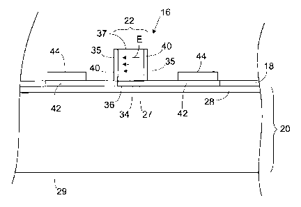
each on one of the branch waveguides. A second splitter and/or combiner 68
combines the
branch signals into an output signal on the output waveguide.
[0070] A first modulator 70 is configured to modulate the branch signal on
one of the
branch waveguides and a second modulator 72 is configured to modulate the
branch signal on
the other branch waveguide. The first modulator and the second modulator can
be configured
as disclosed above and can each be operated as a phase modulator. By
controlling the phase
differential between the light signals on the branch waveguides, the intensity
of the output
light signal can be modulated. As a result, operating the modulators as a
phase modulator can
result in intensity modulation of the light signals.
[0071] One or more of the branch waveguides can optionally include other
components such as variable optical attenuators 74 for balancing out the
intensity on the
different branch waveguides. Although modulators are shown positioned on each
of the
branch waveguides, only one of the branch waveguides need include a modulator
in order for
intensity modulation to be achieved.
[0072] The optical device can be constructed using fabrication
technologies that are
employed in the fabrication of integrated circuits, optoelectronic circuits,
and/or optical
devices. Figure 5A through Figure 14 illustrate a method of forming an optical
device having
a modulator constructed according to Figure lA through Figure 1F, and Figure
1J. The
method is illustrated using a silicon-on-insulator wafer or chip as the
starting precursor for
the optical device. However, the method can be adapted to platforms other than
the
silicon-on-insulator platform.
[0073] Figure 5A through Figure 5C illustrate a first mask 50 formed on
the
silicon-on-insulator wafer or chip to provide a device precursor. Figure 5A is
a topview of
the device precursor. Figure 5B is a cross-section of the device precursor
shown in Figure
5A taken along the line labeled B. Figure 5C is a cross-section of the device
precursor shown
in Figure 5A taken along the line labeled C. The first mask 50 leaves exposed
a region of the
device precursor where an electro-absorption cavity 52 is to be formed while
the remainder of
the illustrated portion of the device precursor is protected. The electro-
absorption cavity 52
is the region of the device precursor where the electro-absorption medium will
to be formed.
A first etch is then performed so as to form the electro-absorption cavity 52.
The first etch
yields the device precursor of Figure 5A through Figure 5C. The first etch is
performed such
that the seed portion 34 of the light-transmitting medium 18 remains on the
base 20.
Accordingly, the first etch is terminated before the base 20 is reached.
16
CA 02781841 2012-M24
WO 2011/075157 PCT/US2010/002959
[0074] A suitable first mask 50 includes, but is not limited to, a hard
mask such as a
silica mask. A suitable first etch includes, but is not limited to, a dry
etch.
[0075] As shown in Figure 6A through Figure 6C, the electro-absorption
medium 27
is formed in the sensor cavity 52 of Figure 5A through Figure 5C. Figure 6A is
a topview of
the device precursor. Figure 6B is a cross-section of the device precursor
shown in Figure
6A taken along the line labeled B. Figure 6C is a cross-section of the device
precursor shown
in Figure 6A taken along the line labeled C. When the light-transmitting
medium 18 is
silicon and the electro-absorption medium 27 is germanium or germanium-
silicon, the
electro-absorption medium 27 can be grown on the seed portion 34 of the
silicon. After
formation of the electro-absorption medium 27, the first mask 50 can be
removed and the
device precursor can be planarized. Suitable methods for polishing include,
but are not
limited to, a chemical-mechanical polishing (CMP) process.
[0076] A second mask 54 can be formed on the device precursor so as to
provide the
device precursor of Figure 7A through Figure 7C. Figure 7A is a topview of the
device
precursor. Figure 7B is a cross-section of the device precursor shown in
Figure 7A taken
along the line labeled B. Figure 7C is a cross-section of the device precursor
shown in Figure
7A taken along the line labeled C. The second mask 54 is formed such that the
regions where
the ridge of the waveguide is to be formed is protected while the remainder of
the illustrated
portion of the device precursor remains exposed. A suitable second mask 54
includes a hard
mask such as a silica mask.
[0077] A second etch is performed on the device precursor of Figure 7A
through
Figure 7C to provide the device precursor of Figure 8A through Figure 8C.
Figure 8A is a
topview of the device precursor. Figure 8B is a cross-section of the device
precursor shown
in Figure 8A taken along the line labeled B. Figure 8C is a cross-section of
the device
precursor shown in Figure 8A taken along the line labeled C. Since the second
etch etches
the light-transmitting medium 18 and the electro-absorption medium 27
concurrently, the
second etch etches the light-transmitting medium 18 and the electro-absorption
medium 27 to
different depths. For instance, Figure 8B illustrates the electro-absorption
medium 27 etched
deeper than the light-transmitting medium 18. The second etch is performed
through the
electro-absorption medium 27 positioned on either side of the ridge 22 down to
the
underlying light-transmitting medium 18. A suitable second etch includes, but
is not limited
to, a dry etch that can etch both the light-transmitting medium 18 and the
electro-absorption
medium 27.
17
CA 027818412012-84-24
WO 2011/075157 PCT/US2010/002959
[0078] A third mask 56 is formed on the device precursor of Figure 8A
through
Figure 8C as shown by the device precursor of Figure 9A through Figure 9C.
Figure 9A is a
topview of the device precursor. Figure 9B is a cross-section of the device
precursor shown
in Figure 9A taken along the line labeled B. Figure 9C is a cross-section of
the device
precursor shown in Figure 9A taken along the line labeled C. Portions of the
third mask 56
are formed over the second mask 54. The third mask 56 is formed such that the
locations on
the device precursor where taper portions of the recesses are to be formed
remain exposed
while the remaining regions of the illustrated portion of the device precursor
are protected.
The taper portions of the recesses are the portions of the recesses that are
spaced apart from
the ridge 22.
[0079] A third etch is then performed so as to provide the device
precursor of Figure
10A through Figure 10C. Figure 10A is a topview of the device precursor.
Figure 10B is a
cross-section of the device precursor shown in Figure 10A taken along the line
labeled B.
Figure 10C is a cross-section of the device precursor shown in Figure 10A
taken along the
line labeled C. The third etch is performed to about the depth to which the
electro-absorption
medium 27 was etched during the second etch. As a result, the third etch forms
the taper
portions of the recesses 25.
[0080] A suitable third mask 56 includes, but is not limited to, a
photoresist. A
suitable third etch includes, but is not limited to, a dry etch.
[0081] The third mask 56 is removed and doped regions 40, 42 are formed in
the
light-transmitting medium 18 and in the electro-absorption medium 27 so as to
provide the
device precursor of Figure 11A and Figure 11B. Figure 11A is a topview of the
device
precursor. Figure 11B is a cross-section of the device precursor shown in
Figure 11A taken
along the line labeled B. The n-type doped regions can be generated by forming
a doping
mask on the device precursor so the locations of the n-type doped regions are
exposed and the
remainder of the illustrated portion of the device precursor is protected.
High angle dopant
implant processes can be employed to form the n-type doped regions. The doping
mask can
then be removed. The same sequence can then be employed to form the p-type
doped regions.
The p-type doped regions can be formed before the n-type doped regions or the
n-type doped
regions can be formed before the p-type doped regions.
[0082] The second mask 54 is removed from the device precursor of Figure
11A and
Figure 12B and a first cladding 58 is formed on the device precursor so as to
provide the
device precursor of Figure 12. Figure 12 is a cross section of the device
precursor through
the region where the modulator is being formed such as the cross section of
Figure 11B. The
18
CA 027818412012-84-24
WO 2011/075157 PCT/US2010/002959
first cladding 58 is formed such that the portion of the doped regions 42 that
are to be
contacted by the electrical conductors 44 remain exposed and the remainder of
the illustrated
portion of the device precursor are protected by the first cladding 58. A
suitable first
cladding 58 includes, but is not limited to, PECVD deposited silica that is
subsequently
patterned using photolithography.
[0083] The electrical conductors 44 are formed on the device precursor of
Figure 12
so as to provide the device precursor of Figure 13. Figure 12 is a cross
section of the device
precursor through the region where the modulator is being formed such as the
cross section of
Figure 11B. The electrical conductors 44 can be formed so each electrical
conductor 44
extend from one of the doped regions 42, out of the recess 25, and over the
light-transmitting
medium 18. Suitable electrical conductors 44 include metals such as titanium
and aluminum.
The metals can be deposited by sputtering and patterned by photolithography.
[0084] A second cladding 60 can optionally be formed on the device
precursor of
Figure 13 so as to provide the device precursor of Figure 14. Figure 12 is a
cross section of
the device precursor through the region where the modulator is being formed
such as the
cross section of Figure 11B. As is evident in Figure 14, the second cladding
60 can be
patterned such that the second cladding 60 defines contact pads the electrical
conductors 44.
A suitable second cladding 60 includes, but is not limited to, PECVD deposited
SiN that is
subsequently patterned using photolithography. After removing photoresists
formed during
photolithography, the device precursor of Figure 14 can be sintered to form
the optical device.
[0085] The device can be used in conjunction with electronics that are in
electrical
communication with the contact pads. The electronics can apply electrical
energy to the
contact pads. Suitable electronics for operating the above modulators can
include a controller.
A suitable controller includes, but is not limited to, a general purpose
processor, a digital
signal processor (DSP), an application specific integrated circuit (ASIC), a
field
programmable gate array (FPGA) or other programmable logic device, discrete
gate or
transistor logic, discrete hardware components, or any combination thereof
designed to
perform the functions attributed to the electronics. A general-purpose
processor may be a
microprocessor, but in the alternative, the controller may include or consist
of any
conventional processor, microcontroller, or state machine. A controller may
also be
implemented as a combination of computing devices, e.g., a combination of a
DSP and a
microprocessor, a plurality of microprocessors, one or more microprocessors in
conjunction
with a DSP core, or any other such configuration.
19
CA 027818412012-84-24
WO 2011/075157 PCT/US2010/002959
[0086] The electronics can optionally include a memory in communication
with the
controller. The electronics can store data for executing the functions of the
electronics in the
memory. The memory can be any memory device or combination of memory devices
suitable for read and/or write operations.
[0087] In some instances, the electronics include a computer-readable
medium in
communication with the controller. The computer-readable medium can have a set
of
instructions to be executed by the controller. The controller can read and
execute instructions
included on the computer-readable medium. The controller executes the
instructions such
that the electronics perform one or more of the described functions. The
computer-readable
medium cab be different from the memory or can be the same as the memory.
Suitable
computer-readable media include, but are not limited to, optical discs such as
CDs, magnetic
storage diskettes, Zip disks, magnetic tapes, RAMs, and ROMs. Some functions
of the
electronics may be executed using hardware as opposed to executing these
functions in
firmware and/or software.
[0088] The method of Figure 4A through Figure 14 can be adapted to form
the other
embodiment disclosed above. For instance, the structure of Figure 1G can be
generated by
performing the second etch through the electro-absorption medium 27 positioned
on either
side of the ridge 22, and through the underlying light-transmitting medium 18
down to the
base 20. Alternately, the structure of Figure 1H can be generated by stopping
the second etch
before etching through the electro-absorption medium 27 positioned on either
side of the
ridge 22, and leaving a layer of the electro-absorption medium 27 on the
underlying
light-transmitting medium 18.
[0089] Other embodiments, combinations and modifications of this invention
will
occur readily to those of ordinary skill in the art in view of these
teachings. Therefore, this
invention is to be limited only by the following claims, which include all
such embodiments
and modifications when viewed in conjunction with the above specification and
accompanying drawings.