Note: Descriptions are shown in the official language in which they were submitted.
CA 02782896 2012-05-30
WO 2011/069553 PCT/EP2009/066865
1
A dc cower source for a high voltage cower apparatus
TECHNICAL FIELD
The present invention relates to a dc power source for a high voltage
power apparatus connected to a high voltage electrical power system,
the dc power source comprising one or more strings including a
plurality of dc power source members connected in series, and
switches configured to connect and disconnect the strings. By a high
voltage electrical power system should be understood an electrical
system within the range of 3 kV and upwards, preferably in the
range of 10 kV and upwards. By a dc power source should be
understood dc power source members connected in series to be
within the range of 3 kV and upwards. With a power apparatus is
meant an apparatus that is capable of controlling reactive power
and/or active power. Examples of power apparatus are a power
compensator and an uninterruptible power supply (UPS).
BACKGROUND OF THE INVENTION
Within flexible alternating current transmission systems (FACTS) a
plurality of control apparatus are known. One such FACTS apparatus
is a static compensator (STATCOM). A STATCOM comprises a voltage
source converter (VSC) having an AC side connected to a high
voltage electrical power system and a DC side connected to a
temporary electric power storage means such as capacitors. The
CA 02782896 2012-05-30
WO 2011/069553 PCT/EP2009/066865
2
STATCOM can supply reactive power to or absorb reactive power
from the transmission line.
As opposed to the STATCOM, which only compensate for reactive
power, another concept is to connect a dc power source to a
compact STATCOM, and thus being able to perform active power
compensation. The construction may be used e.g. as a spinning
reserve and for compensating for fluctuating energy levels in the
power system.
Today the dc power source is a high voltage battery. Since the
power apparatus is connected to the ac voltage of the high voltage
electrical power system, a plurality of battery cells have to be
connected in series to match the dc voltage of the power apparatus.
Moreover, to obtain the desired active power and duration of the
energy storage, a number of strings including a plurality of battery
cells must be connected in parallel.
Furthermore, in case of a fault, such as a short-circuit, the power
apparatus has to be protected. Consequently, two switches are
provided in each string to disconnect the string in case the
converter, a string, or a part of the string is short-circuited. One
switch is able to disconnect the string from the positive dc rail of the
converter and the other switch is able to disconnect the string from
the negative dc rail of the converter. Each of the switches has to be
rated for the entire converter voltage to be capable of protecting the
power apparatus.
CA 02782896 2012-05-30
WO 2011/069553 PCT/EP2009/066865
3
Up to now, mechanical dc circuit breakers have been used as
switches for connection and disconnection of the strings. However,
the availability of dc circuit breakers is limited and the ratings of
these breakers are considerably low and less than the required
voltage ratings in high voltage electrical power systems. To overcome
this problem mechanical ac circuit breakers with some additional
circuitry, such as a resonance circuit connected in parallel with the
ac circuit breaker, have been used.
A solid-state switch is an electronic switch that, unlike a mechanical
breaker, contains no moving parts. There is a desire on the market
to be able to exchange the mechanical ac circuit breakers with solid
state switches. However, a problem with most of the commercially
available solid-state switches is that they become an open-circuit
when failed, which means that if the solid-state switch fails, the
string which includes the failed switch will be disconnected. As a
consequence the dc power source will have its capability significantly
reduced.
SUMMARY OF THE INVENTION
It is an object of the present invention to provide an attractive
solution to the above mentioned problem.
According to one aspect of the invention this object is achieved by a
dc power source as defined in claim 1.
The dc power source according to the invention is characterized in
that
CA 02782896 2012-05-30
WO 2011/069553 PCT/EP2009/066865
4
- one or more strings in the dc power source includes a
plurality of dc power source units connected in series and solid-state
switches configured to connect and disconnect the strings,
- the solid-state switches are distributed among the power
source units of each string,
- all switches in the string are arranged so that they are turned
on and off simultaneously,
- each switch is connected in parallel with a first controllable
semiconductor in a first direction and connected in parallel with a
second controllable semiconductor in a second direction which is
opposite to the first direction, and
- the dc power source comprises a control unit configured to
bypass a failed switch by triggering the forward biased of the first or
second controllable semiconductor connected to the failed switch in
case a fault in the switch is detected.
An advantage with the dc power source according to the invention is
that the resulting current path when a failed switch has been
bypassed enables the dc power source to remain in operation as
long as redundant switches are available. Another advantage is that
the dc power source is more robust and easier to maintain.
Moreover, since the solid-state switches are distributed in the string
it is possible to reduce the total voltage rating of the switches by 50
percent since in case mechanical dc circuit breakers are used both
the breakers must have a breaking capability that equals the entire
voltage across the dc power source to be able to disconnect the dc
power source from the positive and negative dc rail, respectively.
CA 02782896 2012-05-30
WO 2011/069553 PCT/EP2009/066865
With a dc power source member is meant a small entity capable of
providing dc power, such as a battery cell, a photovoltaic cell, a fuel
cell, a flywheel or a super capacitor. Different types of dc power
source members could also be combined in the dc power source.
5
All switches in the string are arranged so that they are turned on
and off simultaneously, implying that each switch only has to
withstand its corresponding part of the voltage across the dc power
source when the string is disconnected. This embodiment eliminates
the risk for causing over voltages due to some switches turn off
earlier than other in the string.
In accordance with an embodiment of the invention, each solid-state
switch comprises a controllable semiconductor. The solid-state
switch is, for example, an Insulated-Gate Bipolar Transistor (IGBT).
In accordance with an embodiment of the invention, each switch is
provided with a gate control unit configured to detect a fault in the
switch and to bypass the switch by triggering the forward biased of
the first or second controllable semiconductor connected to the
switch upon detecting a fault in the switch.
In accordance with an embodiment of the invention at least one of
the first and second controllable semiconductor comprises a
thyristor. Alternatively, at least one of the first and second
controllable semiconductor is an Insulated-Gate Bipolar Transistor
(IGBT)
CA 02782896 2012-05-30
WO 2011/069553 PCT/EP2009/066865
6
In accordance with an embodiment of the invention, the dc power
source members are battery cells. By using battery cells as dc power
source members it is possible to charge the high voltage dc power
source with energy at occasions when there is excessive power
available in the high voltage electrical power system, to be used at
other occasions when there is a deficit of power in the system.
When a series-connection, for example such as the string described
above, comprises a plurality of solid-state switches it is a desired
feature that failing solid-state switches become stable short-circuits
rather than open circuits. By this feature the remaining system can
continue operating, even though one or more switches have failed,
as long as one or more redundant switches are provided. Most of the
commercially available semiconductor switches, such as ABB HiPakTM
IGBT modules, become an open-circuit when failed. Thus, such
economic devices have to date been unsuitable for systems and in
applications were series connection of devices is required.
Nevertheless, such IGBT devices, despite being an open-circuit when
failed, are widely used for traction and industrial applications and as
a result the costs are considerably lower than short-circuit failure
mode devices such as StakPakTM IGBT Press-Packs. By short-circuit
failure mode devices is meant devices which have an inherent ability
to conduct in the failed (shorted) state. Further, in some products a
plethora of functionalities and intelligence have been integrated in
the modules, e.g. over-current protection, thermal protection,
current chopping e.t.c.
CA 02782896 2012-05-30
WO 2011/069553 PCT/EP2009/066865
7
An advantage with the present invention is its ability to combine the
advantageous properties of the IGBT devices being an open-circuit
when failed mentioned above with those advantageous properties
related to solid-state switches that become stable short-circuits.
In accordance with an embodiment of the invention each switch
comprises a plurality of interconnected controllable semiconductors.
One example of a plurality of interconnected controllable
semiconductors is a plurality of controllable semiconductors
connected in series. This feature makes it possible to use controllable
semiconductors with current ratings that are high enough even
though its voltage ratings are below the requisite. Alternatively, the
plurality of interconnected controllable semiconductors is a plurality of
controllable semiconductors connected in parallel. This feature makes
it possible to use controllable semiconductors with voltage ratings
that are high enough even though its current ratings are below the
requisite.
According to another aspect of the invention this object is achieved
by a method as defined in claim 6.
Such a method comprises the following steps:
- measuring the voltage over each switch,
- detecting whether the voltage over any of the switches is
above a threshold value, and
- performing a bypass of the switch upon detecting that the
voltage over said switch is above a threshold value, by
CA 02782896 2012-05-30
WO 2011/069553 PCT/EP2009/066865
8
triggering its forward biased first or second controllable
semiconductor.
According to another embodiment of the invention the method
further comprises the step:
- disconnecting a string which includes the switch when the
triggered controllable semiconductor is turned-off.
BRIEF DESCRIPTION OF THE DRAWINGS
The present invention will be more fully described by way of
example with reference to the accompanying drawings in which:
Figure 1 shows an embodiment of a dc power source in
accordance with the present invention,
Figure 2a shows a schematic figure of a solid-state switch and
parallel-connected thyristors,
Figure 2b shows a schematic figure of a solid-state switch
comprising two controllable semiconductors connected in series and
parallel-connected thyristors,
Figure 2c shows a schematic figure of a solid-state switch
comprising two controllable semiconductors connected in parallel
and parallel-connected thyristors.
DETAILED DESCRIPTION OF THE INVENTION
CA 02782896 2012-05-30
WO 2011/069553 PCT/EP2009/066865
9
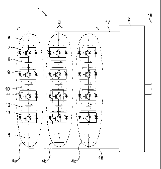
An example of a dc power source according to the invention is
illustrated in figure 1. Figure 1 shows a dc power source 3 for a high
voltage power apparatus 1 connected to a high voltage electrical
power system 19 according to an embodiment of the invention.
Examples of high voltage power apparatus are a power compensator
and an uninterruptible power supply (UPS). High voltage electrical
power systems can be networks for transmission or distribution of
electrical energy as well as industries, hospitals and such. The same
reference numerals are used throughout the figures for same or
corresponding parts. The power apparatus 1 comprises a high
voltage dc power source 3 and a voltage source converter 2. To be
able to produce and absorb not only reactive power but also active
power, the dc power source 3 is connected to the dc side of the
voltage source converter 2. The ac side of the converter is connected
to the high voltage electrical power system 19.
The dc power source 3 comprises one or more strings 4a-c
connected in parallel, the number of strings depending on the desired
amount of active power. In the example illustrated in figure 1, three
strings 4a-c are shown. Each string 4a-c comprises a plurality of dc
power source units 8, 10, 12. The dc power source units 8, 10, 12 in
turn comprises a plurality of series-connected dc power source
members (not shown in figure 1). The total number of dc power
source members in each string 4a-c depends on the voltage level of
the voltage source converter 2 to which they are connected and the
voltage level of the dc power source members used in the string 4a-
c. The dc power source members can be of different types, such as
CA 02782896 2012-05-30
WO 2011/069553 PCT/EP2009/066865
battery cells, photovoltaic cells, fuel cells and super capacitors. These
different types could also be combined.
In each string 4a-c a plurality of solid-state switches 7, 9, 11, 13 are
5 distributed among dc power source units 8, 10, 12. Examples of
solid-state switches are IGBTs, GTOs, IGCTs and MOSFETs. Each dc
power source unit 8, 10, 12 is provided with a solid-state switch 9,
11, 13 configured to connect and disconnect the corresponding dc
power source unit 8, 10, 12. The voltage of the dc power source
10 units 8, 10, 12 is adapted to be below the breaking capability of the
switches 9, 11, 13. All switches 7, 9, 11, 13 in the string are
arranged so that they are turned on and off simultaneously, implying
that each switch 7, 9, 11, 13 only has to withstand the voltage over
its corresponding dc power source unit 8, 10, 12 when the string 4a-
c is disconnected.
Each switch 7, 9, 11, 13 comprises a controllable semiconductor, in
this embodiment a transistor 14 having collector, an emitter and a
gate, and a rectifying member, in this embodiment a diode 15,
which is connected in anti-parallel with the transistor 14, which
makes it possible to charge the dc power source with power from the
high voltage electrical power system 19 whenever excessive power
is available. Connected to the gate of the transistor 14 is a gate
control unit 21 (not shown in figure 1). The gate control unit 21
controls the current through the transistor 14 and is therefore able
to turn the switch on (connect) or off (disconnect). In parallel with
the switch is a first and second controllable thyristor 16, 20
connected. The first controllable thyristor 16 is connected in a first
CA 02782896 2012-05-30
WO 2011/069553 PCT/EP2009/066865
11
direction and the second controllable thyristor 20 is connected in a
second direction which is opposite to the first direction. In case a
fault in the switch 7, 9, 11, 13 is detected by the gate control unit,
the gate control unit performs a bypass of the failed switch by
triggering the forward biased of the first 16 or second 20 thyristor
connected to the failed switch 7, 9, 11, 13. Alternatively, a control
unit which is common to several or all switches in the string or even
the entire dc power source can be used.
To be able to connect and disconnect the strings, the number of
remaining switches (not yet failed) has to exceed a certain amount
depending on the voltage level of the dc power source and the
breaking capability of the remaining switches. For this reason each
string preferable comprises one or more redundant switches
enabling the dc power source to remain in operation despite failed
switches.
It is necessary to disconnect the strings 4a-c from the converter 2
prior to service and maintenance on the dc power source 3 or on the
converter 2, as well as during faults. However, a short-circuit current
occurring internally, inside the dc power source units 8, 10, 12, may
occur. Due to the fact that the switches 9, 11, 13 are distributed
along the string 4a-c, the risk of internal short-circuits will be
decreased and the internal short-circuits still occurring within a dc
power source unit 8, 10, 12 will give lower short-circuit currents
since the number of series-connected dc power source members will
be lower.
CA 02782896 2012-05-30
WO 2011/069553 PCT/EP2009/066865
12
In case of a short-circuit between the negative side of the dc power
source unit 8 closest to positive dc rail 17 and the dc rail 17 itself, a
switch 7 is necessary in the path of the short-circuit current to be
able to disconnect the dc power source unit 8. Thus, an extra switch
7 has been connected to the positive side of the dc power source
unit 8, as shown in figure 1. The switch 7 also has a function as a
redundant switch in case another switch 9, 11, 13 in the string fails.
Disconnectors 5, 6 are placed in the strings next to the positive dc
rail 17 and in the strings next to the negative dc rail 18. The
disconnectors 5, 6 can be advantageous for security reasons during
maintenance work on the dc power source 3 or on the converter 2.
It would also be possible to distribute a plurality of smaller
disconnectors along each string analogously to the distribution of the
switches 7, 9, 11, 13.
In figure 2a a schematic diagram of the solid-state switches 7, 9, 11,
13 and parallel-connected thyristors (16, 20) is shown. Connected to
the gate of the transistor 14 is the gate control unit 21. The gate
control unit controls the transistor 14 by varying the voltage
between the gate and emitter, thereby controlling the resistance
between the collector and the emitter and, thus, the current through
the transistor 14 at a certain voltage can be determined.
In Figure 2b a switch 7, 9, 11, 13 comprising two controllable
semiconductors 14 connected in series and parallel-connected
thyristors (16, 20) is shown. It is however possible to connect three
or more such semiconductors 14 in series. Using a series connection
CA 02782896 2012-05-30
WO 2011/069553 PCT/EP2009/066865
13
makes is possible to use semiconductors with lower voltage ratings
than otherwise feasible.
In Figure 2c a switch 7, 9, 11, 13 comprising two controllable
semiconductors 14 connected in parallel and parallel-connected
thyristors (16, 20) is shown. It is however possible to connect three
or more such semiconductors 14 in parallel. Using a parallel
connection makes is possible to use semiconductors with lower
current ratings than otherwise feasible.