Note: Descriptions are shown in the official language in which they were submitted.
CA 02783416 2012-07-20
METHOD AND SYSTEM OF FABRICATING PZT NANOPARTICLE INK BASED
PIEZOELECTRIC SENSOR
BACKGROUND
1) Field of the Disclosure
The disclosure relates generally to methods and systems of fabricating
sensors,
and more particularly, to methods and systems for fabricating nanoparticle
piezoelectric
sensors deposited onto a structure.
2) Description of Related Art
Small sensors, such as microsensors, may be used in a variety of applications
including in structural health monitoring (SHM) systems and methods to
continuously
monitor structures, such as composite or metal structures, and to measure
material
characteristics and stress and strain levels in order to assess performance,
possible damage,
and current state of the structures. Known SHM systems and methods may include
the use of
small, stiff, ceramic disk sensors integrated onto a polyimide substrate and
connected to
power and communication wiring. Such known sensors are typically manually
bonded to a
structure with an adhesive. Such manual installation may increase labor and
installation costs
and such adhesive may degrade over time and may result in the sensor
disbonding from the
structure. In addition, such known sensors may be made of rigid, planar,
and/or brittle
materials that may limit their usage, for example, usage on a curved or non-
planar substrate
surface may he difficult. Moreover, in a large array of such known sensors,
the amount of
power and communication wiring required may increase the complexity and the
weight of the
structure.
In addition, known sensor systems and methods, such as micro-electromechanical
systems (MEMS) and methods, may include the use of depositing onto a substrate
1
CA 02783416 2012-07-20
piezoelectric sensors, such as lead zirconate titanate (PZT) sensors, having
nanoparticles.
Known methods for making such MEMS may include molten salt synthesis of PZT
powder
for direct write inks. However, the applications of the PZT sensors fabricated
with such
known methods may be limited by the physical geometry of the PZT sensors. Such
physical
geometry limitations may result in inadequate sensing capacities or inadequate
actuation
responses. Further, the PZT sensors fabricated with such known methods may be
unable to be
applied or located in areas where their function may be important due to the
PZT sensor
fabrication method. For example, known molten salt synthesis methods may
require
processing at higher temperatures than certain application substrates can
tolerate.
Further, such known MEMS systems and methods may also include the use of
sensors having nanoparticles which have not been crystallized and which may be
less
efficient than nanoparticles which have been crystallized. Non-crystallized
structures
typically have greater disorganization resulting in decreased response
sensitivity to strain and
voltage, whereas crystallized structures typically have greater internal
organization resulting
in increased response sensitivity to strain and decreased necessity for energy
to operate. In
addition, the nanopartieles of the sensors may be too large for some known
deposition
processes and systems, such as a jetted atomized deposition (JAD) process, and
such
nanoparticles may require a high temperature sintering/crystallization process
which may
result in damage to temperature sensitive substrates or structures.
Accordingly, there is a need in the art for an improved method and system of
fabricating PZT piezoelectric sensors having nanoparticles that may be used in
structural
health monitoring systems and methods for structures, where such improved
method and
system provide advantages over known methods and systems.
2
CA 02783416 2012-07-20
SUMMARY
This need for a method and system of fabricating lead zirconate titanate (PZT)
piezoelectric sensors having nanoparticles that may be used in structural
health monitoring
systems and methods for structures is satisfied. As
discussed in the below detailed
description, embodiments of the method and system may provide significant
advantages over
existing methods and systems.
In an embodiment of the disclosure, there is provided a method of fabricating
a
lead zirconate titanate (PZT) nanoparticle ink based piezoelectric sensor. The
method
comprises formulating a PZT nanoparticle ink. The method further comprises
depositing the
PZT nanoparticle ink onto a substrate via an ink deposition process to form a
PZT
nanoparticle ink based piezoelectric sensor.
In another embodiment of the disclosure, there is provided a method of
fabricating a lead zirconate titanate (PZT) nanoparticle ink based
piezoelectric sensor. The
method comprises formulating a PZT nanoparticle ink comprising pre-
crystallized PZT
.. nanoparticles. The method further comprises suspending the PZT nanoparticle
ink in a sol-
gel based adhesion promoter. The method further comprises depositing the PZT
nanoparticle
ink onto a substrate via a direct write printing process to form a PZT
nanoparticle ink based
piezoelectric sensor.
In another embodiment of the disclosure, there is provided a system for
fabricating a lead zirconate titanate (PZT) nanoparticle ink based
piezoelectric sensor. The
system comprises a formulated PZT nanoparticle ink. The system further
comprises an ink
deposition apparatus depositing the PZT nanoparticle ink onto a substrate to
form a PZT
nanoparticle ink based piezoelectric sensor. The structure may have a non-
curved or planar
surface, a curved or non-planar surface, or a combination of a non-curved or
planar surface
3
and a curved or non-planar surface. The PZT nanoparticle ink based
piezoelectric sensor
may be deposited onto a surface of the structure with one or more layers of
insulation,
coatings, or paint in between a body of the structure and the PZT nanoparticle
ink based
piezoelectric sensor.
In another embodiment of the disclosure, there is provided a method of
fabricating a lead zirconate titanate (PZT) nanoparticle ink based
piezoelectric sensor, the
method comprising: formulating a lead zirconate titanate (PZT) nanoparticle
ink comprising
pre-crystallized PZT nanoparticles; and depositing the PZT nanoparticle ink
onto a substrate
via an ink deposition process to form the PZT nanoparticle ink based
piezoelectric sensor,
wherein the PZT nanoparticle ink comprises one of a sol-gel based adhesion
promoter for
promoting adhesion of the PZT nanoparticle ink to the substrate and a polymer
based
adhesion promoter for promoting adhesion of the lead zirconate titanate
nanoparticle ink to
the substrate.
In another embodiment of the disclosure, there is provided a system for
fabricating a lead zirconate titanate (PZT) nanoparticle ink based
piezoelectric sensor, the
system comprising: a formulated lead zirconate titanate (PZT) nanoparticle ink
comprising
pre-crystallized PZT nanoparticles; and an ink deposition apparatus depositing
the PZT
nanoparticle ink onto a substrate to form the PZT nanoparticle ink based
piezoelectric sensor,
wherein the PZT nanoparticle ink comprises one of a sol-gel based adhesion
promoter for
promoting adhesion of the PZT nanoparticle ink to the substrate and a polymer
based
adhesion promoter for promoting adhesion of the lead zirconate titanate
nanoparticle ink to
the substrate.
4
CA 2783416 2018-05-24
In another embodiment of the disclosure, there is provided a method of
fabricating a lead zirconate titanate (PZT) nanoparticle ink based
piezoelectric sensor, the
method comprising: formulating a lead zirconate titanate (PZT) nanoparticle
ink; depositing
the PZT nanoparticle ink onto a substrate via an ink deposition direct write
printing process
to form the PZT nanoparticle ink based piezoelectric sensor, the PZT
nanoparticle ink
comprising already-grown PZT crystals formed in absence of high temperature
sintering and
crystallization process once deposited; and coupling the PZT nanoparticle ink
based
piezoelectric sensor to a power and communication wire assembly formed of a
conductive
ink deposited onto the substrate via the ink deposition direct write printing
process.
In another embodiment of the disclosure, there is provided a method of
fabricating a lead zirconate titanate (PZT) nanoparticle ink based
piezoelectric sensor, the
method comprising: formulating a lead zirconate titanate (PZT) nanoparticle
ink comprising
pre-crystallized PZT nanoparticles; suspending the PZT nanoparticle ink in a
sol-gel based
adhesion promoter; depositing the PZT nanoparticle ink onto a substrate via a
direct write
printing process to form the PZT nanoparticle ink based piezoelectric sensor,
the PZT
nanoparticle ink comprising already-grown PZT crystals formed in absence of
high
temperature sintering and crystallization process once deposited; and coupling
the PZT
nanoparticle ink based piezoelectric sensor to a power and communication wire
assembly
formed of a conductive ink deposited onto the substrate via the direct write
printing process.
4a
CA 2783416 2018-05-24
In another embodiment of the disclosure, there is provided a system for
fabricating a
lead zirconate titanate (PZT) nanoparticle ink based piezoelectric sensor, the
system
comprising: a formulated lead zirconate titanate (PZT) nanoparticle ink; an
ink deposition
direct write printing apparatus depositing the PZT nanoparticle ink onto a
substrate to form
.. the PZT nanoparticle ink based piezoelectric sensor, the PZT nanoparticle
ink comprising
already-grown PZT crystals formed in absence of high temperature sintering and
crystallization process once deposited; and a power and communication wire
assembly
coupled to the PZT nanoparticle ink based piezoelectric sensor and foimed of a
conductive
ink deposited onto the substrate via the ink deposition direct write printing
apparatus.
In another embodiment of the disclosure, there is provided a structure
comprising: a substrate; and a direct write deposited lead zirconate titanate
(PZT)
nanoparticle ink based piezoelectric sensor assembly deposited on the
substrate, the PZT
nanoparticle ink based piezoelectric sensor assembly comprising: a PZT
nanoparticle ink
deposited onto the substrate via an ink deposition direct write printing
process, the PZT
nanoparticle ink not requiring a high temperature sintering/crystallization
process once
deposited; and a power and communication wire assembly coupled to the PZT
nanoparticle
ink, the power and communication wire assembly comprising a conductive ink
deposited
onto the substrate via the ink deposition direct write printing process.
4b
CA 2783416 2019-03-25
=
In another embodiment of the disclosure, there is provided a composite
structure
comprising: a composite substrate; and a direct write deposited lead zirconate
titanate (PZT)
nanoparticle ink based piezoelectric sensor assembly deposited on the
composite substrate,
the PZT nanoparticle ink based piezoelectric sensor assembly comprising: a PZT
nanoparticle ink based piezoelectric sensor comprising a PZT nanoparticle ink
deposited onto
the composite substrate via an ink deposition direct write printing process,
the PZT
nanoparticle ink not requiring a high temperature sintering/crystallization
process once
deposited; and a power and communication wire assembly coupled to the PZT
nanoparticle
ink based piezoelectric sensor, the power and communication wire assembly
comprising a
conductive ink deposited onto the composite substrate via the ink deposition
direct write
printing process.
In another embodiment of the disclosure, there is provided a metallic
structure
comprising: a metallic substrate; a direct write deposited lead zirconate
titanate (PZT)
nanoparticle ink based piezoelectric sensor assembly deposited on the metallic
substrate, the
.. PZT nanoparticle ink based piezoelectric sensor assembly comprising: a PZT
nanoparticle
ink based piezoelectric sensor comprising a PZT nanoparticle ink deposited
onto the metallic
substrate via an ink deposition direct write printing process, the PZT
nanoparticle ink not
requiring a high temperature sintering/crystallization process once deposited;
and a power
and communication wire assembly coupled to the PZT nanoparticle ink based
piezoelectric
sensor, the power and communication wire assembly comprising a conductive ink
deposited
onto the metallic substrate via the ink deposition direct write printing
process; and an
insulation layer deposited between the metallic substrate and the PZT
nanoparticle ink based
piezoelectric sensor of the direct write deposited lead zirconate titanate
(PZT) nanoparticle
ink based piezoelectric sensor assembly.
4c
CA 2783416 2019-03-25
The features, functions, and advantages that have been discussed can be
achieved
independently in various embodiments of the disclosure or may be combined in
yet other
embodiments further details of which can be seen with reference to the
following description
and drawings.
BRIEF DESCRIPTION OF THE DRAWINGS
The disclosure can be better understood with reference to the following
detailed
description taken in conjunction with the accompanying drawings which
illustrate preferred
and exemplary embodiments, but which are not necessarily drawn to scale,
wherein:
FIG. 1 is an illustration of a perspective view of an exemplary aircraft for
which
.. one of the embodiments of the system and method of the disclosure may be
used;
FIG. 2 is an illustration of a cross-sectional view of one of the embodiments
of a
deposited PZT nanoparticle ink based piezoelectric sensor assembly;
FIG. 3 is an illustration of a cross-sectional view of another one of the
embodiments of a deposited PZT nanoparticle ink based piezoelectric sensor
assembly;
FIG. 4 is an illustration of a top perspective view of one of the embodiments
of a
deposited PZT nanoparticle ink based piezoelectric sensor assembly deposited
on a
composite structure;
4d
Date Recue/Date Received 2020-06-05
CA 02783416 2012-07-20
FIG. 5 is an illustration of a block diagram of one of the embodiments of a
system for fabricating a PZT nanoparticle ink based piezoelectric sensor of
the disclosure;
FIG. 6A is an illustration of a schematic view of one of the embodiments of an
ink deposition process and apparatus for fabricating a PZT nanoparticle ink
based
.. piezoelectric sensor of the disclosure;
FIG. 6B is an illustration of a close-up view of the PZT piezoelectric
nanoparticle
ink based sensor being deposited on the substrate;
FIG. 7 is an illustration of a schematic diagram of one of the embodiments of
a
structural health monitoring system using the PZT nanoparticle ink based
piezoelectric
sensors of the disclosure;
FIG. 8 is an illustration of a flow diagram of an embodiment of a method of
the
disclosure;
FIG. 9 is an illustration of a flow diagram of another embodiment of a method
of
the disclosure; and,
FIG. 10 is an illustration of a block diagram of embodiments of the ink
deposition
processes and ink deposition apparatuses that may be used to fabricate the PZT
nanoparticle
ink based piezoelectric sensor of the disclosure.
DETAILED DESCRIPTION
Disclosed embodiments will now be described more fully hereinafter with
reference to the accompanying drawings, in which some, but not all of the
disclosed
embodiments are shown. Indeed, several different embodiments may be provided
and should
not be construed as limited to the embodiments set forth herein. Rather, these
embodiments
CA 02783416 2016-06-29
are provided so that this disclosure will be thorough and complete and will
fully convey the
scope of the disclosure to those skilled in the art. The following detailed
description is of the
best currently contemplated modes of carrying out the disclosure.
Now referring to the Figures, FIG. 1 is an illustration of a perspective view
of an
exemplary prior art aircraft 10 for which one of the embodiments of a system
100 (see FIG.
5), a method 200 (see FIG. 8), or a method 250 (see FIG. 9), for fabricating a
lead zirconate
titanate (PZT) nanoparticle ink based piezoelectric sensor 110 (see FIG. 2)
for a structure 30,
such as composite structure 102 (see FIG. 1) or a metallic structure 132 (see
FIG. 3), may be
used. As used herein, the term "PZT" means lead zirconate titanate - a
piezoelectric,
ferroeleetric, ceramic material composed of the chemical elements lead and
zirconium and
the chemical compound titanate which may be combined under high temperatures.
PZT
exhibits favorable piezoelectric properties. As used herein, the term
"piezoelectric" in
relation to PZT means that PZT develops a voltage or potential difference
across two of its
faces when deformed, which is advantageous for sensor applications, or it
physically changes
shape when an external electric field is applied, which is advantageous for
actuator
applications. For purposes of this application, the term "feiToelectric" in
relation to PZT
means PZT has a spontaneous electric polarization or electric dipole which can
be reversed in
the presence of an electric field.
The aircraft 10 comprises a fuselage 12, a nose 14, a cockpit 16, wings 18
operatively coupled to the fuselage 12, one or more propulsion units 20, a
tail vertical
stabilizer 22, and one or more tail horizontal stabilizers 24. Although the
aircraft 10 shown in
6
CA 02783416 2012-07-20
FIG. 1 is generally representative of a commercial passenger aircraft, the
system 100 and
methods 200, 250 disclosed herein may also be employed in other types of
aircraft. More
specifically, the teachings of the disclosed embodiments may be applied to
other passenger
aircraft, cargo aircraft, military aircraft, rotorcraft, and other types of
aircraft or aerial
vehicles, as well as aerospace vehicles such as satellites, space launch
vehicles, rockets, and
other types of aerospace vehicles. It may also be appreciated that embodiments
of systems,
methods and apparatuses in accordance with the disclosure may be utilized in
other vehicles,
such as boats and other watercraft, trains, automobiles, trucks, buses, and
other types of
vehicles. It may also be appreciated that embodiments of systems, methods and
apparatuses
in accordance with the disclosure may be utilized in architectural structures,
turbine blades,
medical devices, electronic actuation equipment, consumer electronic devices,
vibratory
equipment, passive and active dampers, or other suitable structures.
In an embodiment of the disclosure, there is provided a system 100 for
fabricating the lead zirconate titanate (PZT) nanoparticle ink based
piezoelectric sensor 110.
FIG. 5 is an illustration of a block diagram of one of the embodiments of the
system 100 for
fabricating the PZT nanoparticle ink based piezoelectric sensor 110 (see also
FIG. 2) of the
disclosure. As shown in FIG. 5, the system 100 for fabricating the PZT
nanoparticle ink
based piezoelectric sensor 110 comprises a formulated lead zirconate titanate
(PZT)
nanoparticle ink 104. The PZT nanoparticle ink 104 comprises nanoscale PZT ink
particles
or nanoparticles 106. Preferably, the nanoscale PZT ink nanoparticles are pre-
crystallized.
The PZT nanoparticle ink 104 preferably has a nanoscale PZT particle size in a
range of from
about 20 nanometers to about 1 micron. The nanoscale PZT ink particles size
allows for the
PZT nanoparticle ink 104 to be deposited using a wide range of ink deposition
processes,
apparatuses, and systems, and in particular, allows for the PZT nanoparticle
ink 104 to be
deposited using a jetted atomized deposition process 126 (see FIGS. 6A and 10)
system and a
7
CA 02783416 2012-07-20
jetted atomized deposition apparatus 146 (see FIGS. 6A and 10). The PZT
nanoparticle ink
based piezoelectric sensor 110 may have a thickness in a range of from about 1
micron to
about 500 microns. The thickness of the PZT nanoparticle ink based
piezoelectric sensor 110
may be measured in terms of a factor of nanoparticle size of the PZT
nanoparticics and the
thickness of conductive electrodes 114, 118 (see FIG. 2). Thickness of the PZT
nanoparticle
ink based piezoelectric sensor 110 may also depend on the size of the PZT
nanoparticle ink
based piezoelectric sensor 110, as a proper aspect ratio may increase the
sensitivity of the
PZT nanoparticle ink based piezoelectric sensor 110.
The PZT nanoparticle ink 104 may further comprise a sol-gel based adhesion
promoter 108 (see FIG. 5) for promoting adhesion of the PZT nanoparticle ink
104 to a
substrate 101. Alternatively, the PZT nanoparticle ink 104 may further
comprise a polymer
based adhesion promoter such as an epoxy or another suitable polymer based
adhesion
promoter. The nanoscale PZT ink nanoparticles 106 may be suspended in a silica
sol-gel and
then deposited using an ink deposition process 122 such as a direct write
printing process
124. The silica sot-gel in the PZT nanoparticle ink formulation enables the
PZT nanoparticle
ink 104 to bond to a wider variety of substrates than certain known adhesion
promoters. Thc
PZT nanoparticle ink based piezoelectric sensor 110 preferably has modalities
based on
ultrasonic wave propagation and electromechanical impedance.
The formulated lead zirconate titanate (PZT) nanoparticle ink 104 may be
formulated by methods disclosed in contemporaneously filed U.S. nonprovisional
patent
application Serial Number 13/211,554, titled ''METHODS FOR FORMING LEAD
ZIRCONATE TITANATE NANOPARTICLES", having Attorney Docket Number UWOTL-
1-37259, filed on August 17, 2011.
8
CA 02783416 2012-07-20
In particular, in such disclosure, methods for forming lead zirconate titanate
(PZT) nanoparticles are provided. The PZT nanoparticles are formed from a
precursor
solution -comprising a source of lead, a source of titanium, a source of
zirconium, and a
mineraliser - that undergoes a hydrothermal process according to the following
reaction ("the
hydrothermal process"):
Pb2-' + + (1-x)ZrO2 + 20H- PbTyri,03 + H20
In the provided methods, the properties of the formed PZT nanoparticles are
dictated at least
by the mineraliser concentration, processing time, heating rate, and cooling
rate.
In one aspect, a method is provided for forming a plurality of PZT
nanoparticles
(also referred to herein as "nanocrystals"). In one embodiment, the method
includes the steps
of: (a) providing an aqueous precursor solution comi5rising a mineraliser
solution, a source
of titanium, a source of zirconium, and a source of lead; and (b) heating the
precursor
solution to produce PZT nanoparticles, wherein heating the precursor solution
comprises a
first heating schedule that includes at least the sequential steps of: (i)
heating the precursor
solution at a first rate to a first temperature, wherein said first rate is
between about 1 C/min
(degrees Celsius per minute) and about 30 C/min, and wherein said first
temperature is
between about 120 C and about 350 C; (ii) holding for a first hold time at the
first
temperature, wherein said first hold time is between about 5 to about 300
minutes; and
(iii) cooling at a second rate to provide a nanoparticle PZT solution
comprising a suspended
plurality of perovskite PZT nanoparticles having a smallest dimension of
between about
20 nm (nanometer) and about 1000 run, wherein said second rate is between
about PC/min
and about 30 C/min.
9
CA 02783416 2012-07-20
Precursor Solution. The precursor solution is defined by reactants that are
processed to form PZT nanoparticles. Specifically, the precursor solution
includes at least a
source of titanium, a source of zirconium, a source of lead, and a
mineraliser. The precursor
solution optionally includes additional solvents or stabilizers, as will be
discussed in more
detail below.
The components of the precursor solution may all be combined simultaneously in
a single reaction vessel, or may be combined stepwise, depending on the
character of the
components of the precursor solution and a potential need to minimize
interaction between
the components of the precursor prior to hydrothermal reaction to produce PZT
nanoparticles.
For example, the source of titanium and the source of zinc may be combined to
form a
precursor gel, which is then combined with a source of lead in aqueous form
and the
mineraliser to provide the precursor solution. Such an approach allows for
maximum control
over the relative molar amounts of each of the reactants (i.e., the sources of
titanium,
zirconium, and lead).
The sources of lead, titanium, and zirconium are present in the precursor
solution
in molar amounts sufficient to obtain PZT nanoparticles having the formula
Pb,(ZiyTi,03,
wherein x is between 0.8 and 2, wherein y is between 0.4 and 0.6, and wherein
y plus z
equals 1. For
example, a common formula for perovskite PZT nanoparticles is
Pb(Zr0.52Ti0,48)03. However, it will be appreciated by those of skill in the
art that the
relative amounts of lead, zirconium, and titanium can be modified within the
provided ranges
to produce the desired characteristics of PZT nanoparticles.
The source of titanium in the precursor solution can be any titanium-
containing
compound that allows for the formation of PZT particles according to the
method provided
CA 02783416 2012-07-20
=
herein. In one embodiment, the source of titanium is Ti[OCH(CH3)214.
Additional sources of
titanium may comprise TiO2, Ti02*nH20, Ti(OC4Hg), Ti(NO3)2, TiC13, TiC14.
The source of zirconium in the precursor solution can be any
zirconium-containing compound that allows for the formation of PZT particles
according to
the method provided herein. In
one embodiment, the source of zirconium is
Zr[O(CH2)7CH3]4. Additional sources of zirconium may comprise Zr(NO3)4*5H20,
ZrOC12*8H20, Zr02*nH20, ZrO2.
The source of lead in the precursor solution can be any lead-containing
compound that allows for the formation of PZT particles according to the
method provided
herein. In one embodiment, the source of lead is Pb(CH3COOH)2. Additional
sources of lead
may comprise Pb(NO3)2, Pb(OH)2, Pb0, Pb203, PbO2.=
In certain embodiments, excess lead is added to the precursor solution. As
used
herein, the term "excess lead" refers to a ratio amount greater than one for
the source of lead.
Excess lead is a means for exerting further control over the characteristics
of the PZT
nanoparticles. Typically, the excess lead is achieved in the precursor
solution by adding an
excess amount of the same source of lead as described above. For example, if
the source of
lead is lead acetate trihydrate, any amount of lead acetate trihydrate added
to the precursor
solution that results in the ratio of the lead acetate trihydrate to be
greater than one compared
to the source of zirconium and the source of titanium will be considered an
excess amount of
lead. In certain embodiments, the excess amount of lead comes from a second,
different,
source of lead.
Excess lead does not alter the chemical composition of the PZT nanoparticles,
but
instead modifies the hydrothermal reaction conditions to produce several
desirable effects on
11
CA 02783416 2012-07-20
the formed PZT nanoparticles. While the excess lead does not alter the
fundamental crystal
structure of the PZT nanoparticles, it improves morphology, reduces amorphous
byproducts,
and reduces the degree of agglomeration between particles.
One less desirable side effect of excess lead is that it also leads to the
formation
of a lead oxide compound that is an impurity. However, the lead oxide impurity
can be
removed by washing the formed PZT nanoparticles with an appropriate solvent
(e.g., diluted
acetic acid).
The mineraliser in the precursor solution facilitates the formation of PZT
during
the hydrothermal process. The mineraliser acts as a source of hydroxide ions
to facilitate the
hydrothermal synthesis of PZT. Representative mineralisers include KOH, NaOH,
LiOH,
NH4OH, and combinations thereof. The concentration of the mineraliser, in a
mineraliser
solution prior to adding to the other components of the precursor solution, is
from about
0.2 M to about 15 M if the mineraliser is liquid such as NaOH. If the
mineraliser is solid,
such as KOH, DI water is first added into the Zr, Ti, Pb mixture and then the
solid
mineraliser is added. The optimal mineraliser concentration depends on the
conditions of the
hydrothermal process, as is known to those of skill in the art.
The concentration of the mineraliser affects the size of PZT nanoparticles
produced. For example, similar PZT nanoparticles formed using 5 M and 10 M KOH
mineraliser have similar morphology, but 5 M mincraliscr results in smaller
nanoparticles
than those formed with 10 M mineraliser, if all other processing conditions
are the same.
In certain embodiments, a stabilizer is added to the precursor to prevent
gelation
and/or precipitation of certain components of the precursor prior to the
hydrothermal process.
That is, stabilizers may be required to maintain all of the necessary
components of the
precursor in solution prior to the hydrothermal process. For example, in one
embodiment,
12
CA 02783416 2012-07-20
acetylacetone ("AcAc") is added to the source of titanium (e.g., titanium
isopropoxide) to
prevent gelation and precipitation prior to reaction to form PZT. In another
embodiment,
propoxide is added to the source of titanium.
The precursor solution is typically aqueous, although it will be appreciated
that
any other solvent capable of solvating the components of the precursor
solution and
facilitating the formation of PZT nanoparticles can also be used. Alternatives
to water may
comprise aqueous solution, mixture of water and organic solvent, or weak
organic acid, for
example, ethylenediamine, CH2C12, ammonium salt, acetic acid or another
suitable
alternative.
In an exemplary embodiment, the precursor solution comprises KOH as the
mineraliser solution, titanium isopropoxide as the source of titanium,
zirconium n-propoxide
as the source of zirconium, lead acetate trihydrate as the source of lead,
acetylacetone as a
stabilizer, and water. The lead acetate trihydrate, zirconium n-propoxide, and
titanium
isopropoxide are present in the precursor in a weight ratio of from about 1 to
about 2 parts
lead acetate trihydrate, from about 0.5 to about 1 parts zirconium n-
propoxide, and from
about 0.8 to about 1.6 parts titanium isopropoxide. The KOH mineraliser
solution is from
about 0.2 to about 15 M.
Heating Schedule. PZT nanoparticles are formed through hydrothermal
processing of the precursor solution. The hydrothermal process includes a
heating schedule
comprising a heating ramp to a first temperature, a hold at the first
temperature, and a cooling
ramp to room temperature.
The heating schedule is performed under pressure greater than 1 atm
(atmosphere).
Accordingly, the precursor solution is contained within an apparatus
configured to both heat and pressurize. In certain embodiments, the pressure
applied during
13
CA 02783416 2012-07-20
the heating schedule is from about 1 atm to about 20 atm. In an exemplary
embodiment, the
precursor solution is contained within an autoclave and autogenous pressure
builds in the
autoclave over the course of the heating schedule. Alternatively, a constant
pressure can be
provided by a pump or other apparatus known to those of skill in the art.
In one embodiment, heating the precursor solution to produce PZT nanoparticles
includes at least the sequential steps of: (i) heating the precursor solution
at a first rate to a
first temperature, wherein said first rate is between about 1 C/min (degrees
Celsius per
minute) and about 30 C/min, and wherein said first temperature is between
about 120 C and
about 350 'V; (ii) holding for a first hold time at the first temperature,
wherein said first hold
time is between about 5 minutes to about 300 minutes; and, (iii) cooling at a
second rate to
provide a nanoparticle PZT solution comprising a suspended plurality of
perovskite PZT
nanoparticles having a smallest dimension of between about 20 nm (nanometers)
and about
1000 nm, wherein said second rate is between about 1 C/min and about 30 C/min.
The heating ramp rate ("first rate") is used to raise the temperature of the
precursor solution from about room temperature (TRT) to the maximum
hydrothermal
processing temperature (Tmõ). The first rate is from about 1 C/min and about
30 C/min.
The processing temperature ("first temperature"; Tmõ) is between about 120 C
(Celsius) and about 350 C. In certain embodiments, the first temperature is
200 C or less.
While the heating schedule is primarily described herein as including a single
first
temperature, to which the solution is heated, it will be appreciated that the
disclosed method
contemplates variations in the first temperature that may arise from the
hydrothermal reaction
or inaccuracies in the heating equipment. Furthermore, the heating step of the
heating
schedule may include second, third, or further, temperatures to which the
heated precursor
14
CA 02783416 2012-07-20
solution is subjected. The second, third, or further temperatures may be
higher or lower than
the first temperature, as required to produce the desired PZT nanoparticles.
The first rate is particularly important to control the size of the PZT
nanoparticles
produced. In this regard, as the temperature of the precursor solution heats
from TRT to
Tmax, there is an intermediate temperature, T at which PZT crystals begin
to nucleate
("Nucleation Zone"). Optimal PZT crystal growth occurs at Tmax, and any
crystals nucleated
at a temperature lower than Tina, will likely grow larger with bigger
aggregates and/or higher
degree of agglomeration than PZT crystals nucleated at Tmax.
A slow ramp rate results in a longer amount of time that the precursor
solution
spends between Tnõc and Tmax. Accordingly, a slow ramp rate results in more
PZT crystal
nucleation at temperatures below Tmax, resulting in inconsistent PZT crystal
size and crystal
structure. As used herein, the term "slow ramp rate" refers to a ramp rate of
below 1 C/min.
Conversely, a relatively fast ramp rate results in homogeneous PZT crystal
nucleation by passing the precursor solution quickly through the temperature
range between
Tõc and Tmax. As used herein, the term "fast ramp rate" refers to a ramp rate
of 10 C/min
or greater. In certain embodiments, the high ramp rate is a ramp rate of 20
C/min or greater.
As a result of the nucleation dynamics described above, the higher the ramp
rate,
the smaller the PZT particles generated. While the heating ramp rate affects
the size and
number of PZT crystals, it does not affect the crystal structure. Similarly,
the cooling rate
does not affect the crystal structure.
The "hold" step of the heating schedule allows the PZT crystals time to form
and
grow. The hold step is between about 5 minutes and about 300 minutes at the
first
CA 02783416 2012-07-20
temperature. Typically, a longer hold time results in larger crystals. Holding
time is
preferably to allow the crystals to grow. If the holding time is too short,
the end product may
not have PZT composition.
After the hold step, the heating schedule proceeds to a "cooling" step. The
cooling rate reduces the temperature from the maximum processing temperature
to room
temperature at a "second rate." The range of the cooling rate is from about 1
C/min to about
30 C/min. The cooling rate impacts several aspects of the PZT nanoparticles.
The cooling
rate partially determines the morphology and size of the formed PZT
nanoparticles. A
relatively fast cooling rate, for example, a cooling rate of greater than 20 C
per minute,
results in PZT nanoparticles in the range of 100 nm to 500 nm and a distinct
cubic shape.
Additionally, a relatively fast cooling rate results in FLA' nanoparticles
that are
physically bonded, as opposed to chemically bonded. Physically bonded PZT
nanoparticles
are preferable to those that are chemically bonded because separation of
physically bonded
nanoparticles is accomplished more readily than the separation of chemically
bonded
nanoparticles (e.g., by mechanical agitation). Finally, a faster cooling rate
minimizes the
presence of PbTiO3 phase in the final product. This is desirable because
PbTiO3 not only is
an impurity that must be removed to obtain pure PZT nanoparticles, but forming
PbTiO3 also
reduces the yield of the FL,"f-formation reaction by consuming lead and
titanium in a form
other than PZT.
In certain embodiments, the second rate is sufficiently large that PZT
particles are
formed that are non-perovskite forms of PZT. In this regard, in certain
embodiments, the
method further comprises a step of treating the nanoparticle PZT solution to
eliminate the
non-perovskite forms of PZT. Such a treatment may include chemically-assisted
dissolution,
wet etching, acid washing, base washing, and combinations thereof Any method
that
16
CA 02783416 2012-07-20
=
selectively eliminates (e.g., dissolves) the non-perovskite PZT can be used.
For example, a
dilute acetic acid wash can be used to eliminate the PbTiO3 non-perovskite
component of the
PZT hydrothermal synthesis.
Alternatively, instead of eliminating the non-perovskite PZT particles, in
certain
embodiments, the method further includes a step of separating the perovskite
PZT
nanoparticles from the non-perovskitc forms of PZT in the nanoparticle PZT
solution. The
end suspension is washed with DI water, diluted acid, or ethanol to remove the
non-
perovskite fornis.
In certain embodiments, the second rate is sufficiently large that the
nanoparticle
PZT solution becomes supersaturated. Nucleation and crystal growth is allowed
when the
solution is supersaturated and they stop when the concentration reaches to an
equilibrium. For
all temperatures, there is an equilibrium concentration responses to it.
Therefore, when the
second rate is slow, the solution can be supersaturated multiple times and the
crystal can have
a greater opportunity to grow bigger. For a fast second rate, the initial
concentration can be
way above equilibrium and the high concentration may promote second nucleation
to occur
along with crystal growth. Nucleation rate is high when the concentration is
high, so both
nucleation and growth are rapid. Because of that, most likely the secondary
nucleation and
growth will not form stable crystals or create amorphous, which can be
removed.
The route to forming the smallest and highest quality PZT nanoparticles is
.. achieved using the shortest possible processing time for the hydrothermal
processing, which
includes using the highest heating ramp rate, the fastest cooling ramp rate,
and a "medium"
mineraliser concentration, since the required processing time will he
different if the
mineraliser concentration is changed. For example, if 5M mineraliser is used,
the processing
time can be as short as one (1) hour but for 2M mineraliser, the required
processing time is
17
CA 02783416 2012-07-20
=
three (3) hours. If the mineraliser concentration is lower at 0.4M, no PZT
will be formed
regardless of the processing time.
After the cooling step, a PZT nanoparticle solution is obtained. The PZT
nanoparticle solution contains a plurality of PZT nanoparticles suspended in
water. The PZT
nanoparticle solution can be filtered or otherwise manipulated to isolate the
PZT
nanoparticles. Depending on the efficiency of the hydrothermal process, the
solution may
also contain PbTiO3, PbZr03, Pb0, TiO2, ZrO2, KOH or other potential
impurities. Washing
the solution with acetic acid is one method for removing Pb0. Excess lead
samples may be
washed with acetic acid.
As shown in FIG. 5, the system 100 further comprises an ink deposition
apparatus 142 (see also FIG. 6A) that deposits the PZT nanoparticle ink 104
onto a substrate
101 to form the PZT nanoparticle ink based piezoelectric sensor 110. The ink
deposition
apparatus 142 and an ink deposition process 122 using the ink deposition
apparatus 142 do
not require growth of PZT crystals 166 (see FIG. 6B) on the substrate 101.
Because the PZT
crystals 166 have already been grown in the PZT nanoparticles, the PZT
nanoparticle ink 104
does not require a high temperature sintering process once deposited during
the ink
deposition process 122. The ink deposition apparatus 142 preferably comprises
a direct write
printing apparatus 144 (see FIG. 10). FIG. 10 is an illustration of a block
diagram of
embodiments of the ink deposition apparatuses and processes that may be used
to fabricate
the PZT nanoparticle ink based piezoelectric sensor 110 of the disclosure. As
shown in FIG.
10, the direct write printing apparatus 144 may comprise a jetted atomized
deposition
apparatus 146, an ink jet printing apparatus 147, an aerosol printing
apparatus 190, a pulsed
laser evaporation apparatus 192, a flexography printing apparatus 194, a micro-
spray printing
apparatus 196, a flat bed silk screen printing apparatus 197, a rotary silk
screen printing
18
CA 02783416 2012-07-20
=
apparatus 198 or another suitable screen printing apparatus, a gravure
printing apparatus 199
or another suitable press printing apparatus, or another suitable direct write
printing apparatus
144.
The PZT nanoparticle ink 104 may be deposited onto the substrate 101 with the
ink deposition apparatus 142 via an ink deposition process 122 (see FIGS. 6A
and 10). The
ink deposition process 122 preferably comprises a direct write printing
process 124 (see FIG.
10). As shown in FIG. 10, the direct write printing process 124 may comprise a
jetted
atomized deposition process 126, an ink jet printing process 128, an aerosol
printing process
180, a pulsed laser evaporation process 182, a flexography printing process
184, a micro-
spray printing process 186, a flat bed silk screen printing process 187, a
rotary silk screen
printing process 188 or another suitable screen printing process, a gravure
printing process
189 or another suitable press printing, or another suitable direct write
printing process 124.
As shown in FIG. 5, the substrate 101 may have a non-curved or planar surface
136, a curved or non-planar surface 138, or a combination of a non-curved or
planar surface
136 and a curved or non-planar surface 138. As shown in FIG. 2, the substrate
101 may have
a first surface 103a and a second surface 103b. The substrate 101 preferably
comprises a
composite material, a metallic material, a combination of a composite material
and a metallic
material, or another suitable material. As shown in the FIG. 2, the substrate
101 may
comprise a composite structure 102. The composite structure 102 may comprise
composite
materials such as polymeric composites, fiber-reinforced composite materials,
fiber-
reinforced polymers, carbon fiber reinforced plastics (CFRP), glass-reinforced
plastics
(GRP), thermoplastic composites, thermoset composites, epoxy resin composites,
shape
memory polymer composites, ceramic matrix composites, or another suitable
composite
material. As shown in FIG. 3, the substrate 101 may comprise a metallic
structure 132. The
19
CA 02783416 2012-07-20
metallic structure 132 may comprise metal materials such as aluminum,
stainless steel,
titanium, alloys thereof, or another suitable metal or metal alloy. The
substrate 101 may also
comprise another suitable material.
FIG. 6A is an illustration of a schematic view of one of the embodiments of an
ink deposition process 122 and an ink deposition apparatus 142 for fabricating
the PZT
nanoparticle ink based piezoelectric sensor 110 of the disclosure. An
exemplary direct write
printing process 124 and direct write printing apparatus 144 are shown in FIG.
6A, which
shows the jetted atomized deposition process 126 and the jetted atomized
deposition
apparatus 146. As shown in FIG. 6A, nanoscale PZT ink nanoparticles 106 may be
transferred via an inlet 148 into a mixing vessel 150 containing a solvent
152. The nanoscale
PZT ink nanoparticles 106 are preferably mixed with the solvent 152 in the
mixing vessel to
form a PZT nanoparticle ink suspension 154. The PZT nanoparticle ink
suspension 154 may
be atomized by an ultrasonic mechanism 158 to form atomized PZT ink
nanoparticles 156.
The atomized PZT ink nanoparticles 156 may then be transferred through a
nozzle body 160
and directed through a nozzle tip 162 to the substrate 101 for depositing and
printing of the
PZT nanoparticle ink based piezoelectric sensor 110 onto the substrate 101.
FIG. 6B is an illustration of a close-up view of the PZT piezoelectric
nanoparticle
ink based sensor 110 being deposited on the substrate 101. FIG. 6B shows the
atomized PZT
ink nanoparticles 156 in the nozzle body 160 and the nozzle tip 162 being
deposited onto the
substrate 101 to form the PZT nanoparticle ink based piezoelectric sensor 110.
As shown in
FIG. 6B, the PZT nanoparticle ink based piezoelectric sensor or sensors 110
may be
deposited onto the substrate 101 in a customized shape 164, such as letters,
designs, logos, or
insignias, or geometric shapes such as circles, squares, rectangles,
triangles, or other
geometric shapes, or another desired customized shape. The ink deposition
process 122 and
CA 02783416 2012-07-20
the ink deposition apparatus 142 do not require growth of PZT crystals 166 on
the substrate
101. Moreover, the deposited nanoscale PZT ink nanoparticles 106 contain a
crystalline
particle structure that does not require any post processing steps to grow the
crystals. The
PZT nanoparticle ink based piezoelectric sensor 110 may be deposited onto a
surface of the
structure 30 with one or more layers of insulation, coatings, or paint in
between a body of the
structure 30 and the PZT nanoparticle ink based piezoelectric sensor 110.
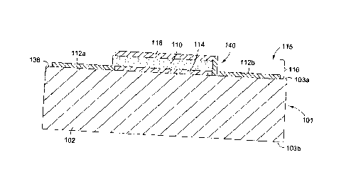
FIGS. 2 and 3 show embodiments of a deposited PZT nanoparticle ink based
piezoelectric sensor assembly 115. FIG. 2 is an illustration of a cross-
sectional view of one
of the embodiments of a deposited PZT nanoparticle ink based piezoelectric
sensor assembly
116 that is deposited onto a substrate 101 comprising a composite structure
102. The
deposited PZT nanoparticle ink based piezoelectric sensor assembly 116
comprises the PZT
nanoparticle ink based piezoelectric sensor 110 coupled to a power and
communication wire
assembly 140 acting as an actuator 141 (see FIG. 4). The power and
communication wire
assembly 140 is preferably formed of a conductive ink 168 (see FIG. 4) that
may be
deposited via the ink deposition apparatus 142 and via/the ink deposition
process 122 onto
the substrate 101. The power and communication wire assembly 140 acting as an
actuator
141 (see FIG. 4) may comprise a first conductive electrode 114, a second
conductive
electrode 118, a first conductive trace wire 112a, and a second conductive
trace wire 112b.
The first conductive electrode 114, the second conductive electrode 118, the
first conductive
trace wire 112a, and the second conductive trace wire 112b may be adjacent to
the PZT
nanoparticle ink based piezoelectric sensor 110.
FIG. 3 is an illustration of a cross-sectional view of another one of the
embodiments of a deposited PZT nanoparticle ink based piezoelectric sensor
assembly 130
that is deposited onto a substrate 101 comprising a metallic structure 132.
The deposited PZT
21
CA 02783416 2012-07-20
nanoparticle ink based piezoelectric sensor assembly 130 comprises the PZT
nanoparticle ink
based piezoelectric sensor 110 coupled to a power and communication wire
assembly 140
acting as an actuator 141 (see FIG. 4). The power and communication wire
assembly 140 is
preferably formed of a conductive ink 168 (see FIG. 4) that may be deposited
via the ink
deposition apparatus 142 and via the ink deposition process 122 onto the
substrate 101. The
power and communication wire assembly 140 acting as the actuator 141 may
comprise the
first conductive electrode 114, the second conductive electrode 118, the first
conductive trace
wire 112a, and the second conductive trace wire 112b. The first conductive
electrode 114,
the second conductive electrode 118, the first conductive trace wire 112a, and
the second
conductive trace wire 112b may be adjacent to the PZT nanoparticle ink based
piezoelectric
sensor 110. As shown in FIG. 3, the deposited PZT nanoparticle ink based
piezoelectric
sensor assembly 130 further comprises an insulation layer 134 deposited
between the
substrate 101 comprising the metallic structure 132 and the PZT nanoparticle
ink based
piezoelectric sensor 110 coupled to the power and communication wire assembly
140. The
insulation layer 134 may comprise an insulating polymer coating, a dielectric
material, a
ceramic material, a polymer material, or another suitable insulation material.
FIG. 4 is an illustration of a top perspective view of the deposited PZT
nanoparticle ink based piezoelectric sensor assembly 115 deposited on a
composite structure
102. FIG. 4 shows a plurality of PZT nanoparticle ink based piezoelectric
sensors 110
coupled to a plurality of power and communication wire assemblies 140, all
deposited on the
composite structure 102. Similarly, for a metallic structure 132, the
deposited PZT
nanoparticle ink based piezoelectric sensor assembly 130 may have a plurality
of PZT
nanoparticle ink based piezoelectric sensors 110 coupled to a plurality of
power and
communication wire assemblies 140, all deposited on the metallic structure
132.
22
CA 02783416 2012-07-20
The deposition of the PZT nanoparticle ink based piezoelectric sensors 110 on
the substrate 101 or structure 30 (see FIG. 7) enables in situ installation of
the PZT
nanoparticle ink based piezoelectric sensors 110 for applications such as
structural health
monitoring. The PZT nanoparticle ink based piezoelectric sensors 110 may be a
key enabler
of high density structural health monitoring systems 170. FIG. 7 is an
illustration of a block
diagram of one of the embodiments of a structural health monitoring system 170
using the
PZT nanoparticle ink based piezoelectric sensors 110 of the disclosure. Two or
more
nanoparticle ink based piezoelectric sensors 110 may be used to enable the
structural health
monitoring system 170 for monitoring structural health 172 of a structure 30,
such as a
composite structure 102 (see FIG. 1) or a metallic structure 132 (see FIG. 3),
or another
suitable structure, and providing structural health data 174. The structural
health data 174
may comprise disbonds, weak bonding, strain levels, moisture ingression,
materials change,
cracks, voids, delamination, porosity, or other suitable structural health
data 174 or
electromechanical properties or other irregularities which may adversely
affect the
.. performance of the structure 30.
The structural health monitoring system 170 preferably comprises a deposited
PZT nanoparticle ink based piezoelectric sensor assembly 115 (see also FIGS. 2
and 3). The
deposited PZT nanoparticle ink based piezoelectric sensor assembly 115 may
comprise the
deposited PZT nanoparticle ink based piezoelectric sensor assembly 116 (see
FIG. 2), if used
with the composite structure 102, and may comprise the deposited PZT
nanoparticle ink
based piezoelectric sensor assembly 130 (see FIG. 3), if used with a metallic
structure 132.
The structural health monitoring system 170 may further comprise a voltage
supply source
176 that may be used for poling the PZT nanoparticle ink based piezoelectric
sensor 110 prior
to use in the structural health monitoring system 170. As used herein, the
term "poling"
means a process by which a strong electric field is applied across a material,
usually at
23
CA 02783416 2012-07-20
=
elevated temperatures, in order to orient or align dipoles or domains. The
voltage supply
source 176 may also drive some PZT nanoparticle ink based piezoelectric
sensors 110 so that
they become actuators 141 sending interrogating signals to other piezoelectric
sensors 110.
As shown in FIG. 7, the structural health monitoring system 170 further
.. comprises an electrical power source 178 for providing electrical power to
the PZT
nanoparticle ink based piezoelectric sensors 110. The electrical power source
178 may
comprise batteries, voltage, RFID (radio frequency identification), magnetic
induction
transmission, or another suitable electrical power source. The electrical
power source 178
may be wireless. As shown in FIG. 7, the system 170 may further comprise a
digital data
!! communications network 179 for retrieving and processing structural
health data 174 from
the PZT nanoparticle ink based piezoelectric sensors 110. The digital data
communications
network 179 may be wireless. The digital data communications network 179 may
retrieve
data received from the 137T nanoparticle ink based piezoelectric sensors 110,
such as with a
receiver (not shown), and may process data received from the PZT nanoparticle
ink based
piezoelectric sensors 110, such as with a computer processor (not shown). The
digital data
communications network 179 may be wireless.
In an embodiment of the disclosure, there is provided a method 200 of
fabricating
a lead zirconate titanate (PZT) nanoparticle ink based piezoelectric sensor
110. FIG. 8 is an
illustration of a flow diagram of an embodiment of the method 200 of the
disclosure. The
.. method 200 comprises step 202 of formulating a lead zirconate titanate
(PZT) nanoparticle
ink 104. The PZT nanoparticle ink 104 comprises nanoscale PZT ink
nanoparticles 106. As
discussed above, the PZT nanoparticle ink 104 preferably has a nanoscale PZT
particle size
in a range of from about 20 nanometers to about 1 micron. The PZT nanoparticle
ink 104
may comprise a sol-gel based adhesion promoter 108 (see FIG. 5) for promoting
adhesion of
24
CA 02783416 2012-07-20
the PZT nanoparticle ink 104 to the substrate 101. The PZT nanoparticle ink
104 is
formulated via the process as discussed in detail above.
The method 200 further comprises step 204 of depositing the PZT nanoparticle
ink 104 onto the substrate 101 via an ink deposition process 122 to form the
PZT nanoparticle
.. ink based piezoelectric sensor 110. The ink deposition process 122
preferably comprises a
direct write printing process 124 (see FIG. 10). As shown in FIG. 10, the
direct write
printing process 124 may comprise a jetted atomized deposition process 126, an
ink jet
printing process 128, an aerosol printing process 180, a pulsed laser
evaporation process 182,
a flexography printing process 184, a micro-spray printing process 186, a flat
bed silk screen
printing process 187, a rotary silk screen printing process 188 or another
suitable screen
printing process, a gravure printing process 189 or another suitable press
printing, or another
suitable direct write printing process.
The substrate 101 preferably comprises a composite material, a metallic
material,
a combination of a composite material and a metallic material, or another
suitable material.
.. The substrate 101 preferably comprises a first surface 103a and a second
surface 103b. The
substrate 101 may have a non-curved or planar surface 136 (see FIG. 5), a
curved or non-
planar surface 138 (see FIG. 5), or a combination of a non-curved or planar
surface 136 (see
FIG. 5) and a curved or non-planar surface 138 (see FIG. 5). The ink
deposition process 122
does not require growth of PZT crystals 166 on the substrate 101. Moreover,
the deposited
nanoscale PZT ink nanoparticles 106 contain a crystalline particle structure
which does not
require any post processing steps to grow the crystals. The PZT nanoparticle
ink based
piezoelectric sensor 110 may be deposited onto the substrate 101 in a
customized shape 164
(see FIG. 6B).
CA 02783416 2012-07-20
The PZT nanoparticle ink based piezoelectric sensor 110 may undergo a poling
process with a voltage supply source 176 (see FIG. 7) prior to being used in
the structural
health monitoring system 170 for monitoring structural health 172 of a
structure 30. The PZT
nanoparticle ink based piezoelectric sensor 110 may be coupled to a power and
communication wire assembly 140 formed from a conductive ink 168 deposited
onto the
substrate 101 via the ink deposition process 122 prior to being used in the
structural health
monitoring system 170. Two or more PZT nanoparticle ink based piezoelectric
sensors 110
may be used to enable the structural health monitoring system 170.
In another embodiment of the disclosure, there is provided a method 250 of
fabricating a lead zirconate titanate (PZT) nanoparticle ink based
piezoelectric sensor 110.
FIG_ 9 is an illustration of a flow diagram of another embodiment of the
method 250 of the
disclosure. The method 250 comprises step 252 of formulating a lead zirconate
titanate (PZT)
nanoparticle ink 104 comprising nanoscale PZT ink nanoparticles 106 that are
pre-
crystallized.
The method 250 further comprises step 254 of suspending the PZT nanoparticle
ink 104 in a sol-gel based adhesion promoter 108. The method 250 further
comprises step
256 of depositing the PZT nanoparticle ink 104 onto a substrate 101 via a
direct write
printing process 124 to form a PZI nanoparticle ink based piezoelectric sensor
110. As
shown in FIG. 10, the direct write printing process 124 may comprise a jetted
atomized
deposition process 126, an ink jet printing process 128, an aerosol printing
process 180, a
pulsed laser evaporation process 182, a flexography printing process 184, a
micro-spray
printing process 186, a flat bed silk screen process 187, a rotary silk screen
process 188 or
another suitable screen printing process, a gravure printing process 189 or
another suitable
press printing, or another suitable direct write printing process 124.
26
CA 02783416 2012-07-20
The substrate 101 preferably comprises a composite material, a metallic
material,
a combination of a composite material and a metallic material, or another
suitable material.
The substrate 101 preferably comprises a first surface 103a and a second
surface 103b. The
substrate 101 may have a non-curved or planar surface 136 (see FIG. 5), a
curved or non-
planar surface 138 (see FIG. 5), or a combination of a non-curved or planar
surface 136 (see
FIG. 5) and a curved or non-planar surface 138 (see FIG. 5). The ink
deposition process 122
does not require growth of PZT crystals 166 on the substrate 101. Moreover,
the deposited
nanoseale PZT ink nanoparticles 106 contain a crystalline particle structure
which does not
require any post processing steps to grow the crystals. The PZT nanoparticle
ink based
piezoelectric sensor 110 may be deposited onto the substrate 101 in a
customized shape 164
(see FIG. 6B).
The PZT nanoparticle ink based piezoelectric sensor 110 may undergo a poling
process with a voltage supply source 176 prior to being used in the structural
health
monitoring system 170 for monitoring structural health 172 of a structure 30.
The PZT
nanoparticle ink based piezoelectric sensor 110 may be coupled to a power and
communication wire assembly 140 formed from a conductive ink 168 deposited
onto the
substrate 101 via the ink deposition process 122 prior to being used in the
structural health
monitoring system 170. Two or more PZT nanoparticle ink based piezoelectric
sensors 110
may be used to enable the structural health monitoring system 170.
The structure 30 may comprise an aircraft, a spacecraft, an aerospace vehicle,
a
space launch vehicle, a rocket, a satellite, a rotorcraft, a watercraft, a
boat, a train, an
automobile, a truck, a bus, an architectural structure, a turbine blade, a
medical device,
electronic actuation equipment, a consumer electronic device, vibratory
equipment, passive
and active dampers, or another suitable structure. The system 100 and methods
200, 250 may
27
CA 02783416 2012-07-20
be used across many industries including, for example, wind power generation
(health
monitoring of turbine blades),
aerospace applications, military applications, medical
applications, electronic actuation equipment, consumer electronic products, or
any
application where structures or materials require a monitoring system.
Embodiments of the system 100 and methods 200, 250 disclosed herein for
fabricating the PZT nanoparticle ink based piezoelectric sensors 110 provide
PZT
nanoparticle ink based piezoelectric sensors 110 that may be used for a
variety of applications
including ultrasonic damage detection for composite and metallic structures,
crack
propagation detection sensors, pressure sensors, or another suitable sensor.
For example, the
PZT nanoparticle ink based piezoelectric sensors 110 of the system 100 and
methods 200,
250 provide cradle to grave health monitoring of various components in
aircraft such as
damage detection for door surrounds, military platforms such as crack growth
detection for
military aircraft, and space systems such as cryo-tank health monitoring. The
PZT
nanoparticle ink based piezoelectric sensors 110 may provide data that was
previously not
available that may influence new and efficient designs which may reduce costs.
Using the direct write printing process 124, and for example, the jetted
atomized
deposition process 126, along with the formulated PZT nanoparticle ink 104,
allows many
PZT nanoparticle ink based piezoelectric sensors 110 to be deposited onto a
substrate 101 or
structure 30 and at a decreased cost as compared to known piezeoelectric
sensors.
Embodiments of the system 100 and methods 200, 250 disclosed herein provide
PZT
nanoparticle ink based piezoelectric sensors 110 that allow for the placement
of the PZT
nanoparticle ink based piezoelectric sensors 110 in numerous areas of a
structure and at large
quantities, both of which may be difficult with known piezoelectric sensors.
28
CA 02783416 2012-07-20
Moreover, embodiments of the system 100 and methods 200, 250 disclosed
herein for fabricating the PZT nanoparticle ink based piezoelectric sensors
110 provide PZT
nanoparticle ink based piezoelectric sensors 110 that are advantageous to
known sensors
because they do not require an adhesive to bond them to the structure, and
this decreases the
possibility that the PZT nanoparticle ink based piezoelectric sensors 110 may
disbond from
the structure. Embodiments of the system 100 and methods 200, 250 disclosed
herein for
fabricating the PZT nanoparticle ink based piezoelectric sensors 110 provide
PZT
nanoparticle ink based piezoelectric sensors 110 that are enabled by the
availability of
nanoscale PZT ink nanoparticles 106 having favorable piezoelectric properties
and that are
deposited onto a substrate or structure in a desired configuration for use
without the use of
adhesive. Because the PZT nanoparticle ink based piezoelectric sensors 110 may
be
deposited onto a substrate or structure with no adhesive between the PZT
nanoparticle ink
based piezoelectric sensors 110 and the substrate or structure, improved
signal coupling into
the structure being interrogated may be achieved. Further, embodiments of the
system 100
and methods 200, 250 disclosed herein for fabricating the PZT nanoparticle ink
based
piezoelectric sensors 110 provide PZT nanoparticle ink based piezoelectric
sensors 110 do
not require manual placement or installation on the substrate or structure and
may be
deposited or printed onto the substrate or structure, along with all the
required power and
communication wire assemblies, thus decreasing labor and installation costs,
as well as
decreasing complexity and weight of the structure. In addition, the PZT
nanoparticle ink
based piezoelectric sensors 110 may be fabricated from numerous direct write
printing
processes, including the jetted atomized deposition process 126; may be
fabricated from
nanoparticle size particles which have been pre-crystallized and may be more
efficient than
known sensors that have not been crystallized; do not require a high
temperature
.. sintering/crystallization process and thus reduce or eliminate possible
damage to temperature
29
CA 02783416 2012-07-20
sensitive substrates or structures; may be deposited onto curved or non-planar
substrates or
structures; have no or minimal physical geometry limitations and thus decrease
the possibility
of inadequate sensing capacities or inadequate actuation responses. Finally,
embodiments of
the system 100 and methods 200, 250 disclosed herein for fabricating the PZT
nanoparticle
ink based piezoelectric sensors 110 provide PZT nanoparticle ink based
piezoelectric sensors
110 that may be used to predict deterioration or weaknesses of a structure
prior to the actual
development of such deterioration or weaknesses, and thus, may increase
reliability of the
structure or structural component parts, and may reduce overall manufacturing
and
maintenance costs over the life of the structure or structural component
parts; and that have
the ability to predict, monitor, and diagnose the integrity, health, and
fitness of a structure
without having to disassemble or remove the structure or drill holes into the
structure for
insertion of any measurement tools.
In the embodiments above, a method is disclosed of fabricating a lead
zirconate
titanate (PZT) nanoparticle ink based piezoelectric sensor 110 including
formulating a lead
zirconate titanate PZT nanoparticle ink 104; and, depositing the PZT
nanoparticle ink 104
onto a substrate 101 via an ink deposition process 122 to form a PZT
nanoparticle ink based
piezoelectric sensor 110. In one instance, the PZT nanoparticle ink 104
includes nanoscale
PZT particles 106. In one variant, the PZT nanoparticle ink 104 includes a sot-
gel based
adhesion promoter for promoting adhesion of the PZT nanoparticle ink 104 to
the substrate
101. The ink deposition process 122 does not require PZT crystal growth on the
substrate
101. In another variant, the ink deposition process 122 includes a direct
write printing
process 124 selected from a group comprising a jetted atomized deposition
process 126, an
ink jet printing process 128, an aerosol printing process 180, a pulsed laser
evaporation
process 182, a flexography printing process 184, a micro-spray printing
process 186, a fiat
bed silk screen printing process 187, a rotary silk screen printing process
188, and a gravure
CA 02783416 2012-07-20
printing process 189. In one variant, the substrate 101 includes a material
selected from a
group comprising a composite material, a metallic material, and a combination
of a
composite material and a metallic material. In one alternative, the substrate
101 has a curved
surface 138. In yet another embodiment, the PZT nanoparticle ink based
piezoelectric sensor
.. 110 is deposited onto the substrate 101 in a customized shape.
In accordance with the embodiments above, a system is disclosed for
fabricating
a lead zirconate titanate (PZT) nanoparticle ink based piezoelectric sensor
110, the system
includes a formulated lead zirconate titanate (PZT) nanoparticle ink 104; and,
an ink
deposition apparatus 142 depositing the PZT nanopartiele ink 104 onto a
substrate 101 to
form a PZT nanoparticle ink based piezoelectric sensor 110. In one instance,
the PZT
nanoparticle ink 104 includes nanoscalc PZT particles 106. In one variant, the
PZT
nanoparticle ink 104 includes a sol-gel based adhesion promoter 108 for
promoting adhesion
of the PZT nanoparticle ink 104 to a surface of the substrate 101. In yet
another variant, the
ink deposition apparatus 142 does not require PZT crystal growth on a surface
of the
substrate 101.
In one alternative, the ink deposition apparatus 142 includes a direct write
printing apparatus 144 selected from a group comprising a jetted atomized
deposition
apparatus 146, an ink jet printing apparatus 147, an aerosol printing
apparatus 190, a pulsed
laser evaporation apparatus 192, a flexography printing apparatus 194, a micro-
spray printing
.. apparatus 196, a flat bed silk screen printing apparatus 197, a rotary silk
screen printing
process 188, and a gravure printing process 189. In another alternative, the
substrate 101
includes a material selected from a group comprising a composite material, a
metallic
material, and a combination of a composite material and a metallic material.
In another
31
CA 02783416 2012-07-20
variant, the PZT nanoparticle ink based piezoelectric sensor 110 is deposited
onto the
substrate 101 in a customized shape.
In still another embodiment, a method is disclosed of fabricating a lead
zirconate
titanate (PZT) nanoparticle ink based piezoelectric sensor. In this method, a
lead zirconate
titanate (PZT) nanoparticle ink is formulated comprising pre-crystallized PZT
nanoparticles.
Furthermore, PZT nanoparticle ink are suspended in a sol-gel based adhesion
promoter; and,
the PZT nanoparticle ink are deposited onto a substrate via a direct write
printing process to
form a PZT nanoparticle ink based piezoelectric sensor. In one variant, the
PZT nanoparticle
ink includes nanoscale PZT particles. In another variant, the direct write
printing process
does not require PZT crystal growth on the substrate.
In yet another embodiment, a system is disclosed for fabricating a lead
zirconate
titanate (PZT) nanoparticle ink based piezoelectric sensor. The system
includes: a formulated
lead zirconate titanate (PZT) nanoparticle ink; and, an ink deposition
apparatus depositing the
PZT nanoparticle ink onto a substrate to form a PZT nanoparticle ink based
piezoelectric
sensor. In one variant, the substrate is curved. In one variant, the PZT
nanoparticle ink based
piezoelectric sensor is deposited onto the substrate in a customized shape.
Many modifications and other embodiments of the disclosure will come to mind
to one skilled in the art to which this disclosure pertains having the benefit
of the teachings
presented in the foregoing descriptions and the associated drawings. The
embodiments
described herein are meant to be illustrative and are not intended to be
limiting or exhaustive.
Although specific terms are employed herein, they are used in a generic and
descriptive sense
only and not for purposes of limitation.
32